

Page 1

high performance GPS multichip module (MCM)
Features
■ GPS multichip module:
– STA2058 TESEO Baseband
– STA5620 RF Front-end
■ Complete embedded memory system:
– Flash 256 KB + 16 Kbytes
– RAM 64 Kbytes.
■ 66-MHz ARM7TDMI 32 bit processor
■ High performance GPS engine (HPGPS)
■ SBAS (WAAS and EGNOS) supported
■ Sensitivity (-146 dBm acquisition, -159 dBm
tracking)
■ Time to first fix (1 s reacquisition, 2.5 s hot start,
34 s warm start, 39 s cold start)
■ Accuracy (2 m autonomous)
■ Extensive GPS receiver interfaces: 32 GPIOs,
4 UARTs, 2 SPIs, 2 I2Cs, 1CANs 2.0,
1 USB 1.1, 1 HDLC and 4 channels ADC
■ Compatible with L1 signal (C/A code)
■ ST proprietary technology
– CMOS Flash embebbed technology for
STA2058
– BiCMOS Sige technology for STA5620
■ LFBGA104 lead-free package
■ -40 °C to 85 °C operating temperature range
Table 1. Device summary
STA8058
TESEO™
Data Brief
LFBGA104 (7x11x1.4 mm)
Evaluation kits
■ STA8058 module reference designs
(17x19 mm and 25x25 mm)
■ Evaluation board hosting STA8058 module
Description
STA8058 TESEO MCM is a fully embedded GPS
engine integrating STA2058 TESEO baseband.
and STA5620 RF front-end. The embedded Flash
memory enables the equipment manufacturer to
load the entire GPS software (including tracking,
acquisition, navigation and data output) after
customising its interfaces to his needs.
A standard GPS library is available from ST. By
combining the ARM7TDMI microcontroller core
with on-chip Flash/RAM, 16-channel GPS
correlator DSP, RF Front-end and an extensive
range of interfaces on single package solution,
the STA8058 provides a highly-flexible and costeffective solution for GPS applications.
Order Code Package Packing Automotive Grade
STA8058 LFBGA104 (7x11x1.4mm) Tray No
STA8058TR LFBGA104 (7x11x1.4mm) Tape and reel No
STA8058A LFBGA104 (7x11x1.4mm) Tray Yes
STA8058ATR LFBGA104 (7x11x1.4mm) Tape and reel Yes
March 2009 Rev 2 1/14
For further information contact your local STMicroelectronics sales office.
www.st.com
14
Page 2

Contents STA8058
Contents
1 Features summary . . . . . . . . . . . . . . . . . . . . . . . . . . . . . . . . . . . . . . . . . . 3
2 Pin description . . . . . . . . . . . . . . . . . . . . . . . . . . . . . . . . . . . . . . . . . . . . . 5
2.1 Logic symbol . . . . . . . . . . . . . . . . . . . . . . . . . . . . . . . . . . . . . . . . . . . . . . . 5
2.2 System block diagram . . . . . . . . . . . . . . . . . . . . . . . . . . . . . . . . . . . . . . . . 6
2.3 LFBGA104 ball out . . . . . . . . . . . . . . . . . . . . . . . . . . . . . . . . . . . . . . . . . . . 9
2.4 Power supply pins . . . . . . . . . . . . . . . . . . . . . . . . . . . . . . . . . . . . . . . . . . . 9
3 Electrical characteristics . . . . . . . . . . . . . . . . . . . . . . . . . . . . . . . . . . . . 11
4 Package information . . . . . . . . . . . . . . . . . . . . . . . . . . . . . . . . . . . . . . . . 12
5 Revision history . . . . . . . . . . . . . . . . . . . . . . . . . . . . . . . . . . . . . . . . . . . 13
2/14
Page 3

STA8058 Features summary
1 Features summary
● ARM7TDMI 16/32 bit RISC CPU based host microcontroller running at a frequency up
to 66 MHz.
● Complete Embedded Memory System:
– Flash 256 Kbytes + 16 Kbytes (100 KB erasing/programming cycles)
– RAM 64 Kbytes.
● 16 channel High performance GPS correlation DSP.
● ST propietary technology:
– CMOS Flash embedded technology for baseband
– BiCMOS Sige for radio front-end
● SBAS (WAAS and EGNOS) supported.
● -40 °C to 85 °C operating temperature range.
● 104-pin LFBGA104 package.
● Power supply:
– 3.0 V to 3.6 V operating supply range for input/output periphery
– 3.0 V to 3.6 V operating supply range for A/D converter reference
– 1.8 V operating supply range for core supply provided by internal voltage regulator
with external stabilization capacitor or by external supply voltage
– 2.4 V to 3 V operating supply range for RF front-end section
● Reset and clock control unit able to provide low power modes (WAIT, SLOW, STOP,
Standby) and to generate the internal clock from the external reference through
integrated PLL.
● 32 programmable general purpose I/O, each pin programmable independently as
digital input or digital output; 30 are multiplexed with peripheral functions; 16 can
generate an interrupt on input level/transition.
● Real time clock module with 32 kHz low power oscillator and separate power supply to
continue running during stand-by mode.
● 16-bit Watchdog timer with 8 bits prescaler for system reliability and integrity.
● One CAN module compliant with the CAN specification V2.0 part B (active) and bit rate
can be programmed up to 1 MBaud.
● Four 16-bit programmable timers with 7 bit prescaler, up to two input capture/output
compare, one pulse counter function, one PWM channel with selectable frequency
each.
● 4 channels 12-bit sigma-delta analog to digital converter, single channel or multi
channel conversion modes, single-shot or continuous conversion modes, sample rate
1 kHz, conversion range 0-2.5V .
● Three serial communication interfaces (UART) allow full duplex, asynchronous,
communications with external devices, independently programmable TX and RX baud
rates up to 625K baud.
● One UART adapted to suit smart card interface needs, for asynchronous SC as defined
by ISO 7816-3. It includes SC clock generation.
● Two serial peripheral interfaces (SPI) allow full duplex, synchronous communications
with external devices, master or slave operation, max baud rate of 5.5Mb/s. One SPI
may be used as multimedia card interface.
3/14
Page 4

Features summary STA8058
● Two I
● Enhanced interrupt controller supports 32 interrupt vectors, independently maskable,
2
C interfaces provide multi-master and slave functions, support normal and fast
2
I
C mode (400 KHz), 7/10 bit addressing modes. One I2C Interface is multiplexed with
one SPI, so either 2 x SPI + 1 x I
2
C or 1 x SPI + 2 x I2C may be used at a time.
with interrupt vector table for faster response and 16 priority levels, software
programmable for each source. Up to 2 maskable interrupts may be mapped on FIQ.
● Wake-up unit allows exiting from powerdown modes by detection of an event on two
external pins (one is active high and other is active low) or on internal Real Time Clock
alarm.
● USB unit V1.1 compliant, software configurable endpoint setting, USB suspend/resume
support
● High level data link controller (HDLC) unit supports full duplex operating mode, NRZ,
NRZI, FM0 and MANCHESTER modes, and internal 8-bit Baud Rate Generator.
● RF front-end features:
– LOW IF (4 MHz) architecture
– Compatible with GPS L1 signal
– VGA gain internally regulated
– On chip programmable PLL
– SPI interface
4/14
Page 5
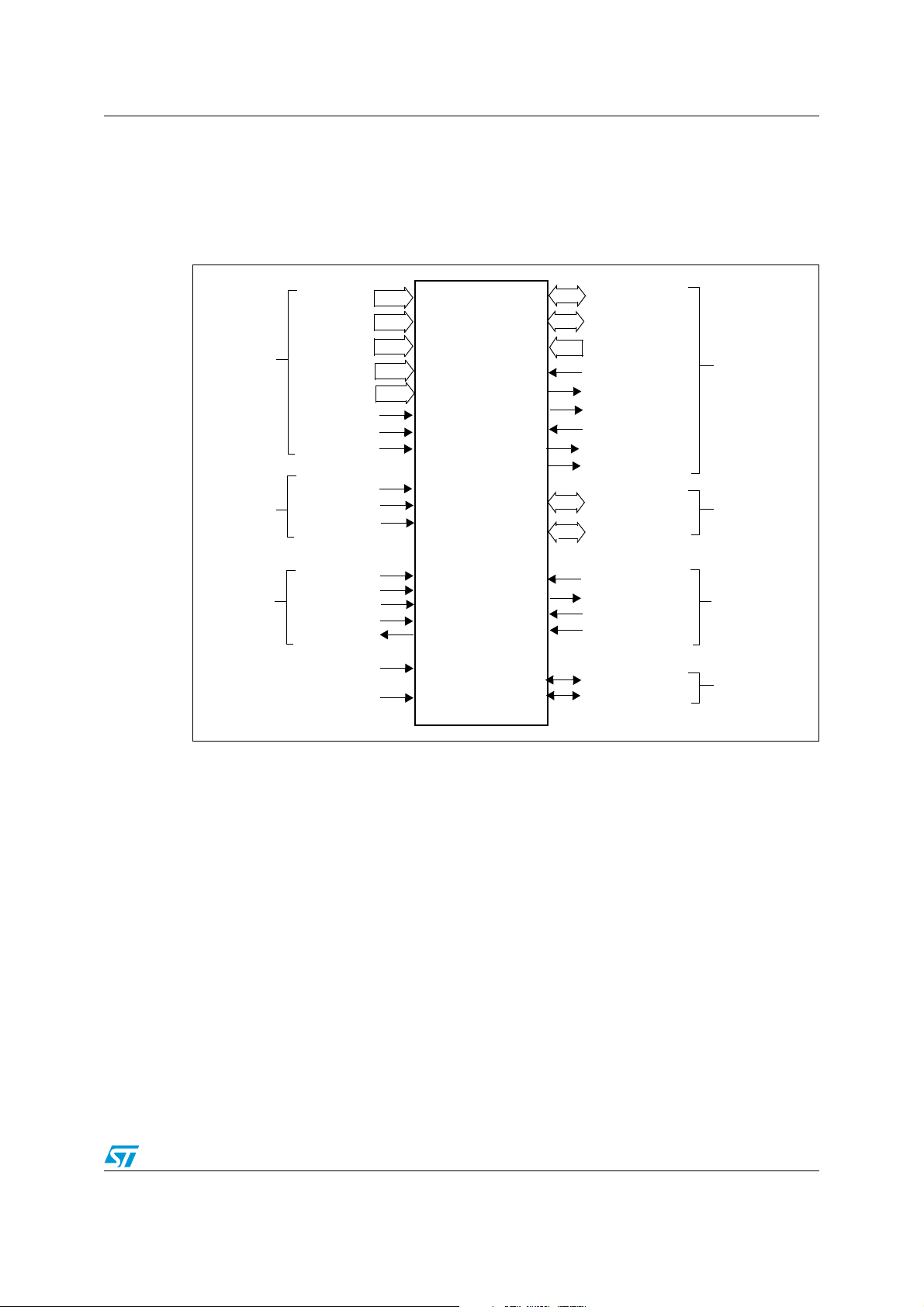
STA8058 Pin description
2 Pin description
2.1 Logic symbol
Figure 1. STA8058 TESEO MCM symbol
Power
Pads
Clock
& Reset
JTAG
Por t
V18 [2]
V33 [7]
V27 [8]
VSS [10]
VSSRF [11]
AVSS
AVD D
V18BKP
GPSCLK
CK
RSTINn
JTDI
JTCK
JTMS
JTRSTn
JTDO
BOOTEN
GPSDAT
TESEO
MCM
Xtal (IN,Out,Clk)
SPI (DI,DO,CS, CLK)
Enable (Chip,RF)
Mode
GPS_CLK
Sign
RF_IN
AGC_CNTR
IF_TEST
P0.[15:0]
P1.[15:0]
nSTDBY_I
RTCXTO
RTCXTI
WAKEUP
USBDP
USBDN
RF Pads
GeneraI
Purpose I/O
RTC
& WKUP
Pads
USB Pads
5/14
Page 6

Pin description STA8058
2.2 System block diagram
Figure 2. STA8058 TESEO baseband block diagram
1 DP
5 DP
3 DP
5 DP
4 AF
2 AF
4 AF
4 AF
ARM7TD
MI
256K
Flash
64KRAM
STC
(JTAG)
VREG
RCCU
PLL
INTERRUPT
CONTR.
12-bit
ADC
TIMER0
TIMER1
TIMER2
TIMER3
ARM7 Native BUS
APB BUS
APB
BRIDGE3
APB
BRIDGE2
HPGPS 16-ch.
correlator +
3 DP
Emerald DSP
APB
BRIDGE1
I2C0
I2C1
SPI0
2 AF
2 AF
4 AF
APB BUS
SPI1
UART0
UART1
4 AF
2 AF
2 AF
2 DP
16 AF
2 AF
32 IO
RTC
OSCILL
Wakeup
WATCH
DOG
Fully Prog.
I/O PORTS
UART2
UART3
[USB]
[CAN]
HDLC
2 AF
2 AF
3 DP
2 AF
3 AF
6/14
Page 7

STA8058 Pin description
/
/
S
/
O
e
C
O
T
Figure 3. STA5620 RF front-end
K
SIGN
MAG
GPS_CL
XTAL_CLK
IF_TES
AGC_CTRL
enabl ed by rf e & sp eci fi c enables
gc e & rfe
CMOS Drivers
if _out _en
IF filt er
2
bi t s
sign
mag
AD
AGC
mag
Combi ner
PFD
CP
gc e
Xtal
samp l e_mod e (1:0)
LO96
gps_clk
R
N
lo48_clk
Vari able
/ 2
/ 48
test _clk
Fil ter
Pol yph ase
IR Mixer
RFA
0˚
90˚
mag
gp s_clk
si gn
Buffer
Test
Logi c
SPI
xc
XIX
Xtal Osc
xt al_clk
Reset
Gen erat or
CHIP_EN
rese t
<chi p co nf ig>
xt al_clk
Interface
hc e
RF_IN
7/14
TEST_EN2
TEST_EN1
TEST_CLK
SPI_C
SPI_DI
SPI_CLK
SPI_D
MODE
RF_EN
Page 8

Pin description STA8058
Figure 4. STA8058 TESEO MCM block diagram
P1.8/PPS
P1.9/PRN
3 Timers [9], ADC[4]
SPI[4], I2C[3], 3 UARTS [6]
USB[3], CAN[2], HDLC[3]
Wake_Up
NRSTIN
NSTDBY_IN
BOOT0, BOOT1, BOOTEN
JTDI,JTCK,JTMS,JTRSTn,JTDO
RTCXTI
RTCXTO
S1_SSN
S1_MOSI
S1_MISO
SPI_DI
SPI_DO
SPI_CS
RF_IN
STA8058 Teseo MCM
The two dice must be interconnected eachother at board level
SAW Filter
S1_SCLK
SPI_CLK
STA2058
Baseband
GPS_Dat
Sign
STA5620
RF Front-End
IF_TEST
MODE
GPIO
CHIP_EN
AGC_CNTR
GPIO
RF_EN
CK
XTAL_CLK
XTAL_IN
TCXO
GPSCLK
GPS_CLK
AVSS
VSSIO_PLL
AVDD V18BKP
V33 [4] V18[2] VSS [4]
V33IO_PLL
VSSRF_IO
VSSRF [10]
VSSRF_A [2]
V33
V27_RF [5]
V27_PLL[4]
VSS18[2]
VSS_BKP
VSS_REG
V33_REG_BKP
LNA
8/14
Page 9

STA8058 Pin description
2.3 LFBGA104 ball out
Table 2. Ball out for LFBGA104 package
A VSS AVSS AVDD V18BKP RTCXTO RTCXTI
P1.2/T3_
B
OCMPA/
AIN.2
P1.1/T3_
C
ICAPA/AI
N.1
V33IO_P
D
LL
VSSIO_PLLP1.8/PPSP1.9/PR
E
P1.11/
F
CANRX
P1.12/
G
CANTX
H VSS
123456789 10111213
VSS18 V18 VSSBKP
P1.0/T3_
OCMPB/
AIN.0
P1.3/T3_
ICAPB/AI
N.3
USBDP
USBDN
P1.13/H
CLK/IO.S
CL
P1.4/T1
_ICAPA
P1.7/T1
_OCMPAVSS VSS JTCK JTDO
N.11
P1.10/U
SBCLK
P0.1/SO
_MOSI/
U3.RX
P1.14/H
RXD/IO.
SDA
P1.5/T1_
ICAPB
P1.6/T1_
OCMPB
P0.3/SO
_SSN/I1.
SDA
P0.0/SO
_MISO/U
3.TX
P1.15/HT
XD
NSTDBY
_IN
NRSTIN
VSS18
V18
P0.7/S1_
SSN
P0.2/SO
_SCLK/I1
.SCL
V33
PO.15/W
AKEUP
P0.13/U2
_RX/T2.
OCMPA
P0.14/U2
_TX/T2.I
CAPA
P0.9/UO
_TX/BO
OT.0
PO.12/S
CCLK
V33RE
G_BKP
VSSREGGPSCL
CK
JTMS JTDI SPI_CS IF_TEST VSSRF VSSRF RF_IN
V33
P0.11/U
1_TX/B
OOT.1
PO.8/U
O_RX/U
0.TX
GPSDA
T
K
P0.5/S1
_MOSI
P0.6/S1
_SCLK
P0.4/S1
_MISO
BOOTE
N
P0.10/U
1_RX/U
1.TX
nJTRST RF_EN
GPS_CLK CHIP_EN V27PLL V27PLL V27PLL
SPI_DI XTAL_CLK VSSRF V27PLL V27RF
SPI_CLK MODE VSSRF VSSRF VSSRF_A
SPI_DO
SIGN V27RF V27RF V27RF VSSRF
V33 VSSRF:IO V33 V27RF VSSRF
AGC_CNT
R
XTAL_O
UT
VSSRF VSSRF VSSRF_A
XTAL_IN VSSRF
2.4 Power supply pins
SS
18
33
- Digital supply voltage for I/O circuitry (3.3 Volt) B6,F7,G10,H9,H11
- Digital ground for I/O circuitry A1,D4,D5,H1
- Digital supply voltage for I/O circuitry and for PLL reference (3.3V) D1
- Digital ground for I/O circuitry and for PLL reference E1
Digital supply voltage for backup block I/O circuitry and for Ballast I/O
(3.3V)
- Digital ground for Ballast I/O B7
Digital supply voltage for core circuitry (1.8 Volt): When using the
internal voltage regulator, this pin shall not be driven by an external
-
voltage supply, but a capacitance of at least 10μF (Tantalum, low
series resistance) + 33nF (ceramic) shall be connected between
these pins and V
to guarantee on-chip voltage stability.
SS18
- Digital ground for core circuitry B2,E5
Digital supply voltage for backup block (RTC, oscillator, Wake-up
controller - 1.8 Volt): when using the internal voltage regulator, this
-
pin shall not be driven by an external voltage supply, but a
capacitance of at least 1μF shall be connected between this pin and
V
to guarantee on-chip voltage stability.
SSBKP
Table 3. Power supply pins
Symbol I/O Function LFBGA104
V
V
V
33IO-PLL
V
SSIO-PLL
V
33REG_BKP
V
SSREG
V
V
SS18
V
18BKP
A7
B3,F5
A4
9/14
Page 10

Pin description STA8058
Table 3. Power supply pins (continued)
Symbol I/O Function LFBGA104
V
SSBKP
AV
DD
AV
SS
V
27RF
V
27PLL
V
SSRF
V
SSRF_A
V
SSRF_IO
Note: V
- Digital ground for backup logic B4
- Analog supply voltage for the A/D converter A3
- Analog supply ground for the A/D converter A2
- Analog supply voltage for RF chain (2.7V)
C13,G10,G11,G12,H
- Analog supply voltage for PLL embedded into RF part (2.7V) B11,B12,B13,C12
A13,C11,D11,D13,
- Analog supply ground for RF core
E11,E12,F11,F12,
G13,H13
- Analog supply ground for RF amplifier D13, F13
- Analog supply ground for RF IO circuirty H10
and V
33
All V
SS
, V
SS18
33IO-PLL
common ground plane, taking care of noise filtering, especially on AV
and V
SSRF_IO
are all internally connected. Same for VSS and V
, V
SSBKP
AVSS,V
,
SSRF,VSSRF_A
and V
SSRF_IO
SSIO-PLL
.
pins must be tied together to the
SS
,V
SSRF
, V
12
SSRF_A
10/14
Page 11

STA8058 Electrical characteristics
3 Electrical characteristics
See STA2058 (Teseo Baseband) and STA5620 (RF Front-end) datasheet for related data.
11/14
Page 12

Package information STA8058
4 Package information
In order to meet environmental requirements, ST offers these devices in different grades of
ECOPACK
®
packages, depending on their level of environmental compliance. ECOPACK
®
specifications, grade definitions and product status are available at: www.st.com.
ECOPACK
®
is an ST trademark.
Figure 5. LFBGA104 (11x7x1.4mm) mechanical data and package dimensions
DIM.
A 1.400 0.0551
A1 0.210 0.008 3
A2 0.990 0.0390
A3 0.200 0.0079
A4 0.800 0.0 315
b 0. 350 0.4 00 0.45 0 0.0138 0.0157 0.0177
D 10.900 11.000 11.100 0.4291 0.4331 0.4370
D1 9.600 0.3780
E 6.900 7.000 7.100 0.2717 0. 2756 0.2 795
E1 5.600 0.2205
e 0.800 0.0315
F 0.700 0. 0276
ddd 0.100 0.0039
eee 0.150 0.0059
fff 0.080 0.0031
mm inch
MIN. TYP. MAX. MIN. TYP. MAX.
OUTLINE AND
MECHANICAL DATA
Body: 11 x 7 x 1.4mm
LFBGA104
Low profile Fine Pitch Ball Grid Array
12/14
8054244 B
Page 13

STA8058 Revision history
5 Revision history
Table 4. Document revision history
Date Revision Changes
25-Oct-2007 1 Initial release.
Updated Table 1: Device summary on page 1.
19-Mar-2009 2
Updated ECOPACK description in Section 4: Package information on
page 12.
13/14
Page 14

STA8058
Please Read Carefully:
Information in this document is provided solely in connection with ST products. STMicroelectronics NV and its subsidiaries (“ST”) reserve the
right to make changes, corrections, modifications or improvements, to this document, and the products and services described herein at any
time, without notice.
All ST products are sold pursuant to ST’s terms and conditions of sale.
Purchasers are solely responsible for the choice, selection and use of the ST products and services described herein, and ST assumes no
liability whatsoever relating to the choice, selection or use of the ST products and services described herein.
No license, express or implied, by estoppel or otherwise, to any intellectual property rights is granted under this document. If any part of this
document refers to any third party products or services it shall not be deemed a license grant by ST for the use of such third party products
or services, or any intellectual property contained therein or considered as a warranty covering the use in any manner whatsoever of such
third party products or services or any intellectual property contained therein.
UNLESS OTHERWISE SET FORTH IN ST’S TERMS AND CONDITIONS OF SALE ST DISCLAIMS ANY EXPRESS OR IMPLIED
WARRANTY WITH RESPECT TO THE USE AND/OR SALE OF ST PRODUCTS INCLUDING WITHOUT LIMITATION IMPLIED
WARRANTIES OF MERCHANTABILITY, FITNESS FOR A PARTICULAR PURPOSE (AND THEIR EQUIVALENTS UNDER THE LAWS
OF ANY JURISDICTION), OR INFRINGEMENT OF ANY PATENT, COPYRIGHT OR OTHER INTELLECTUAL PROPERTY RIGHT.
UNLESS EXPRESSLY APPROVED IN WRITING BY AN AUTHORIZED ST REPRESENTATIVE, ST PRODUCTS ARE NOT
RECOMMENDED, AUTHORIZED OR WARRANTED FOR USE IN MILITARY, AIR CRAFT, SPACE, LIFE SAVING, OR LIFE SUSTAINING
APPLICATIONS, NOR IN PRODUCTS OR SYSTEMS WHERE FAILURE OR MALFUNCTION MAY RESULT IN PERSONAL INJURY,
DEATH, OR SEVERE PROPERTY OR ENVIRONMENTAL DAMAGE. ST PRODUCTS WHICH ARE NOT SPECIFIED AS "AUTOMOTIVE
GRADE" MAY ONLY BE USED IN AUTOMOTIVE APPLICATIONS AT USER’S OWN RISK.
Resale of ST products with provisions different from the statements and/or technical features set forth in this document shall immediately void
any warranty granted by ST for the ST product or service described herein and shall not create or extend in any manner whatsoever, any
liability of ST.
ST and the ST logo are trademarks or registered trademarks of ST in various countries.
Information in this document supersedes and replaces all information previously supplied.
The ST logo is a registered trademark of STMicroelectronics. All other names are the property of their respective owners.
© 2009 STMicroelectronics - All rights reserved
STMicroelectronics group of companies
Australia - Belgium - Brazil - Canada - China - Czech Republic - Finland - France - Germany - Hong Kong - India - Israel - Italy - Japan -
Malaysia - Malta - Morocco - Singapore - Spain - Sweden - Switzerland - United Kingdom - United States of America
www.st.com
14/14
 Loading...