

Page 1
®
STA7056
3W MONO BRIDGE AMPLIFIER
PRODUCT PREVIEW
NO EXTERNAL COMPONENTS
NO POP AT TURN-ON/OFF
LOW POWER CONSUMP TION
SHORT CIRCUIT PROOF
DESCRIPTION
The STA7056 is a mono Bridge Amplifier assembled in single in line 9 pins package.
The STA7056 is specially designed for battery fed
portable recorders, radios and TV receivers.
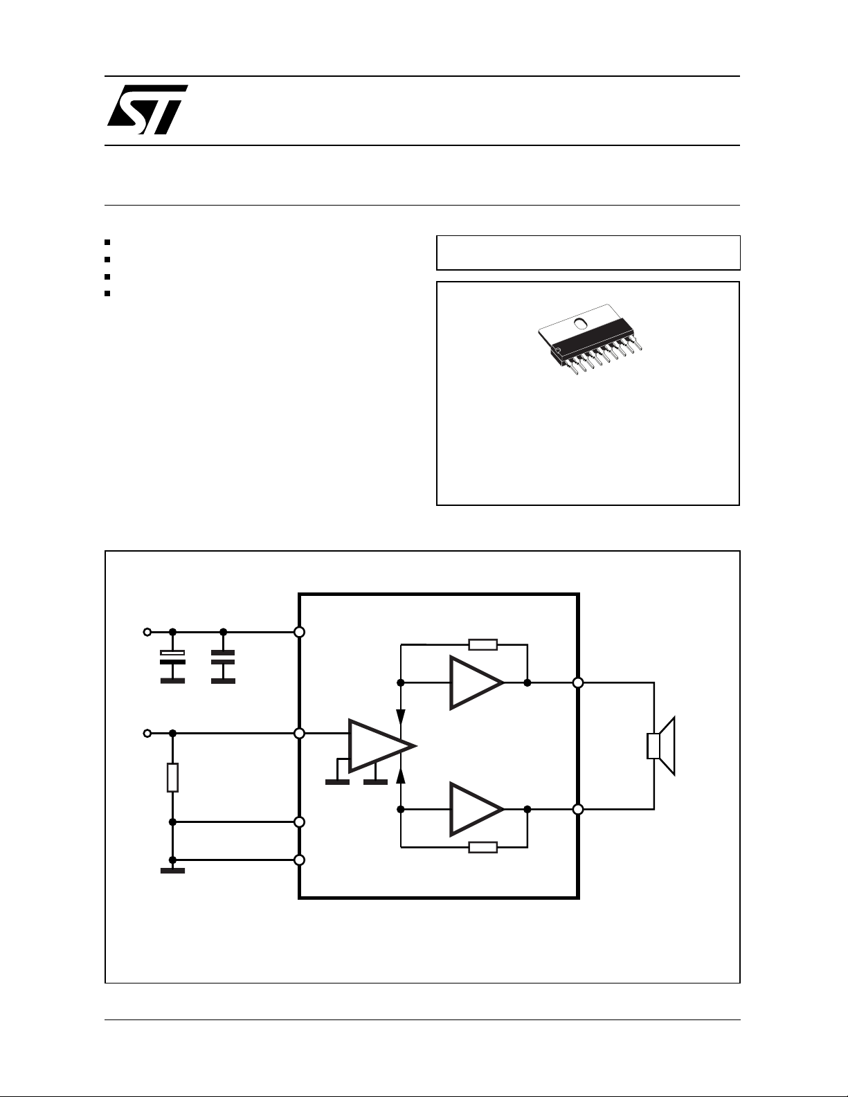
BLOCK DIAGRAM
(1)
VS
2
BI20II TECHNOLOGY
SIP9
ORDERING NUMBER:
STA7056
0.1µF220µF
(+)
6
Vi
3
+
RL 16Ω
-
RS
5KΩ
8
SIGNAL GND
4
(-)
POWER GND
7
D99AU1000B
(1) This capacitor can be omitted if the supply electrolytic capacitor is placed closer to pin 2
March 2000
This is preliminary information on a new product now in development or undergoing evaluation. Details are subject to change without notice.
1/5
Page 2
STA7056
ABSOLUTE MAXIMUM RATINGS
Symbol Parameter Value Unit
V
S
I
O
I
O
P
tot
Tj,T
stg
T
sc
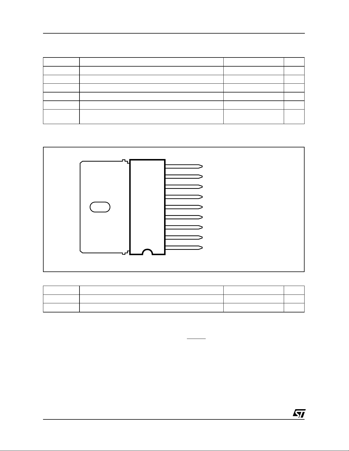
PIN CONNECTION
Supply Voltage 20 V
Output Peak current (repetitive f ≥ 20Hz) 1 A
Output Peak current (non repetitive t = 100µs) 1.5 A
Total Power Dissipation (Tcase <70°C) 10 W
Storage and Function Temperature -40 to 150 °C
Short Circuit Time
(the load can be short circuited to all input conditions)
1hr
9 N.C.
8 OUTPUT(-)
7
6
5
4
3
2
1
SIP9
POWER GROUND
OUTPUT(+)
N.C.
SIGNAL GROUND
INPUT(+)
V
S
N.C.
THERMAL DATA
Symbol Parameter Value Unit
R
th j-case
R
th j-amb
Thermal Resistance Junction-case 8 °C/W
Thermal Resistance Junction-ambient 50 °C/W
Power Dissipation
s
Assume: V
= 11V; RL = 16
The minimum sine-wave dissipation is P
Ω
max =
d
2
V
S
= 1.52W
2
R
L
π
⁄
⋅
2
The Rth j - amb of the package is 50°C/W.
T amb (max) = 150 - 50 x 1.52 = 74°C
2/5
Page 3

STA7056
ELECTRICAL CHARACTERISTICS
amb
= 25°C unless otherwise specified.)
T
(Refer to the test circuit, V
S
= 12V; RL = 16Ω; RS = 50Ω; f = 1KHz,
Symbol Parameter Test Condition Min. Typ. Max. Unit
V
S
I
q
I
O
P
O
Supply Voltage 3 18 V
Total Quiescent Current RL = ∞ 68mA
R
= 16Ω 10 20 mA
L
Repetitive Peak Output Current 0.9 A
Output Power THD = 10%; RL = 16Ω 2.8 3.3 W
THD = 10%; RL = 8Ω 4.5 W
THD Total Harmonic Distortion PO = 0.5W 0.25 1 %
G
v
Voltage Gain 39 40.5 42 dB
|Zin| Input Impedance 100 KΩ
I
i
∆V
SVR Supply Voltage Rejection RS = 0Ω; f = 100Hz to 10 KHz;
Input Bias Current 100 300 nA
DC Output Offset Voltage RS = 5KΩ 250 mV
O
36 50 dB
Vr = 0.2V
Vno Noise Output Voltage R
= 5KΩ; f = 20Hz to 20 KHz; 180 300 µV
S
3/5
Page 4

STA7056
DIM.
MIN. TYP. MAX. MIN. TYP. MAX.
A 7.1 0.280
a1 2.7 3 0.106 0.118
B230.90
B3 24.8 0.976
b1 0.5 0.020
b3 0.85 1.6 0.033 0.063
C 3.3 0.130
c1 0.43 0.017
c2 1.32 0.052
D 21.2 0.835
d1 14.5 0.571
e 2.54 0.100
e3 20.32 0.800
L 3.1 0.122
L1 3 0.118
L2 17.6 0.693
L3 0.25 0.010
L4 17.4 17.85 0.685 0,702
M 3.2 0.126
N 1 0.039
P 0.15 0.006
mm inch
OUTLINE AND
MECHANICAL DATA
SIP9
L4
L2
P
La1
D
L1
M
19
e3
B
B3
C
L3
N
d1
b1
b3
ec1
SIP9
c2
A
4/5
Page 5

STA7056
Information furnished is believed to be accurate and reliable. How ever, STMicroelect ronics assumes no responsibility for the consequences
of use of such information nor for any infringement of patents or other rights of third parties whic h may result from its use. No license is
granted by im plicat ion or otherw ise under any patent o r pa tent r ights of STMic roelec tronics. Spec ifica tion ment ioned in this pu blic ation a re
subject to cha nge without notice. Thi s publication supersedes and re pl aces all information p reviously supplied. STM i croelectroni cs products
are not authorized for use as critical components in life support devices or systems without express written approval of STMicroelectronics.
The ST logo is a registered trademark of STMicroelectronics
© 2000 STMicroelectronics – Printed in Italy – All Rights Reserved
STMicroelect roni cs GROUP OF COMPANIES
Australia - Brazil - China - Finland - France - Germany - Hong Kong - India - Italy - Japan - Malaysia - Malta - Morocco -
Singapore - Spain - Sweden - Switzerland - United Kingdom - U.S.A.
http://www.st.com
5/5
 Loading...