

Page 1
4 X 50W STEREO POWER AMPLIFIER
■
MONOCHIP BRIDG E QUAD CONFIGURABLE
AMPLIFIER OPTIMIZED FOR BASH
ARCHITECTURE
■
4 X 50W OUTPUT POWER @ RL = 8
THD = 10% or (2 x 50W @ 8 Ω + 1 x 100W @
4Ω) or (2 x 100W @ 4 Ω)
■
PRECISION RECTIFIERS TO DRIVE THE
BUCK REGULATOR
■
ON-OFF SEQUENCE/ TIMER WITH MUTE
AND STANDBY
■
PROPORTIONAL OVER POWER OUTPUT
CURRENT TO LIMIT THE BUCK REGULATOR
■
ABSOLUTE POWER BRIDGE OUTPUT
TRANSISTOR POWER PROTECTION
■
ABSOLUTE OUTPUT CURRENT LIMIT
■
INTEGRATED THERMAL PROTECTION
■
POWER SUPPLY OVER VOLTAGE
®
Ω,
STA530
FLEXIWATT27
PROTECTION
■
FLEXIWATT POW ER PAC KAG E WI TH 2 7 PIN
■
BASH® LICENCE REQUIRED
DESCRIPTION
The STA530 is a BASH® power amplifier where
®
BASH
means “High Efficiency”.
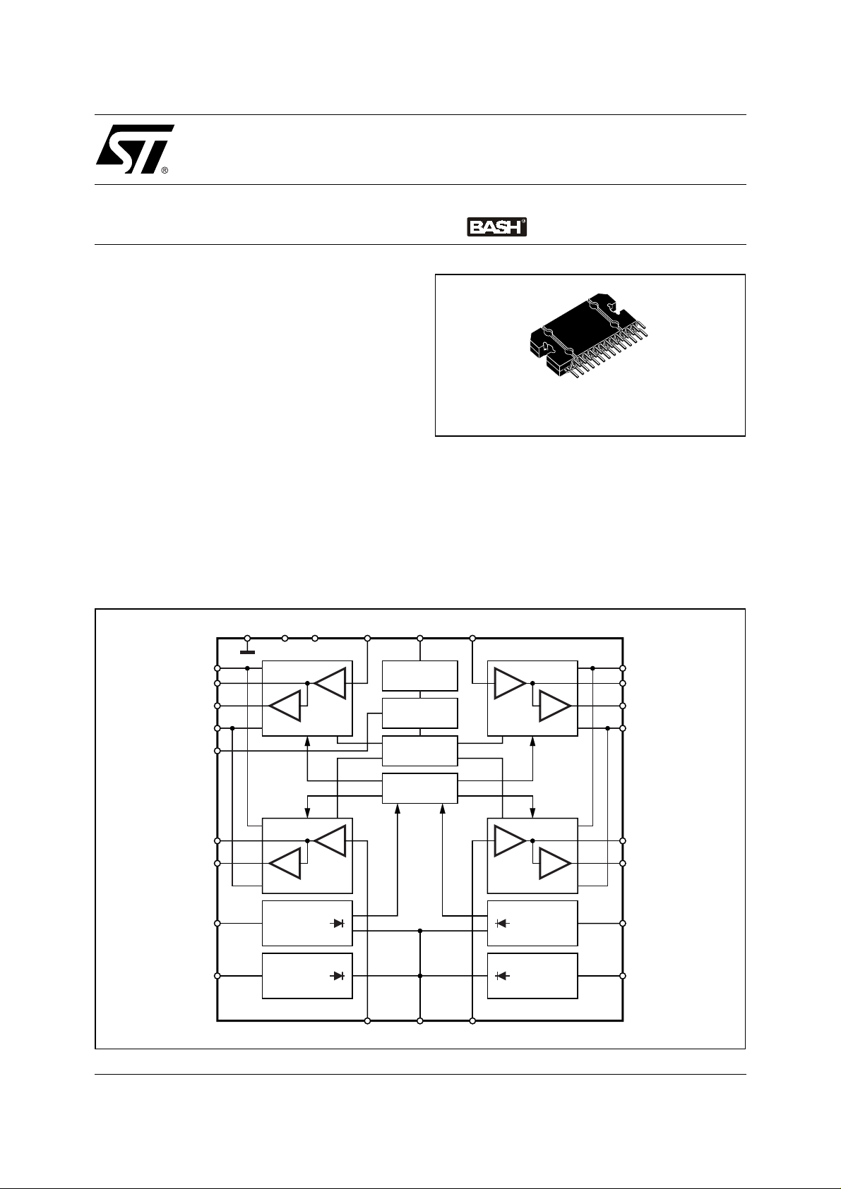
BLOCK DIAGRAM
CD+1&2
OUT1+
OUT1-
CD-1&2
PROT
OUT2+
OUT2-
TRK_2/PAR1&2
TRK_1
S
+10
-1
OUTPUT BRIDGE
+10
-1
OUTPUT BRIDGE
ABSOLUTE
VALUE
BLOCK
ABSOLUTE
VALUE
BLOCK
PWR_INP1GND +VS-V
STBY/MUTE
TURN-ON/OFF
SEQUENCE
PROTECTION
SOA
DETECTOR
CONFIG.
PWR_INP3
+10
-1
OUTPUT BRIDGE
+10
-1
OUTPUT BRIDGE
ABSOLUTE
VALUE
BLOCK
ABSOLUTE
VALUE
BLOCK
CD+3&4
OUT3+
OUT3-
CD-3&4
OUT4+
OUT4-
TRK_4/PAR3&4
TRK_3
July 2003
PWR_INP2
PWR_INP4TRK_OUT
D02AU1344
1/17
Page 2

STA530
DESCRIPTION
(continued)
In fact it's permits to build a BASH® architectur e ampl ifier adding onl y few external components and a va riable
Buck regulator tracking the audio signal. Notice that normally only one Buck regulator is used to supply a multichannel amplifiers sys tem , therefore most of the functions implemented in the cir c uit have a summing output
pin.
The signal circuits are bias ed by fixed negative and posi tive voltages r eferred to Ground. Instead the final stages of the output amplifiers are supplied by two external voltages that are following the audio signal . In this way
the headroom for the output transistors is kept at minimum level to obtain a high efficiency power amplifier.
The circuit contains all the blocks to build a configurable four channel amplifier.
The tracking signal for the external Buck regulator is generated from the Absolute Value Block (AVB) that rec-
tifies the audio signal. The outputs of these bl ocks are decoupled by a diode to per mit an easy sum of this si gnal
for the multichannel application. The gain of the stage AVB is equal to 70 ( +36.9 dB). A sophisticated circuit
performs the output transistor power detector that , with the buck regulator, reduces the power supply voltage .
Moreover, a maximum current output limiting and the over temperature sensor have been added to protect the
circuit itself. The external voltage applied to the STBY/MUTE pin forces the two amplifiers in the proper condition to guarantee a silent turn-on and turn-off.
ABSOLUTE MAXIMUM RATINGS
Symbol Parameter Value Unit
V
V
+V
-V
CD+
CD-
Positive supply voltage referred to pin 14 (GND) 27 V
s
Negative supply voltage referred to pin 14 (GND) -27 V
s
Positive supply voltage tracking rail referred to pin 14 (GND) 20 V
Negative supply voltage referred to -Vs
(1)
-0.3 V
V
CD-
V
PWR_Imp1
V
PWR_Imp2
V
TRK_1
V
TRK_2
V
PWR_Imp 3
V
PWR_Imp 4
V
TRK_3
V
TRK_4
I
STBY-max
V
STBY/
MUTE
Notes: 1. V
Negative supply voltage tracking rail referred to pin 14 (GND) -20 V
Pin 11, 10, 9, 8 Negative & Positive maximum voltage referred to
-25 to +25 V
GND (pin 14)
Pin 17, 18, 19, 20 Negative & Positive maximum voltage referred
-25 to +25 V
to GND (pin 14)
Pin 12 maximum input current (Internal voltage clamp at 5V) 500 µA
Pin 12 negative maximum voltage referred to GND (pin 14) -0.5 V
must not be m ore negativ e than -Vs
CD-
THERMAL DATA
Symbol Parameter Value Unit
T
Max Junction temperature 150 °C
j
R
th j_case
Thermal Resistance Junction to case .............................. ..max 1 °C/W
2/17
Page 3
STA530
OPERATING RANGE
Symbol Parameter Value Unit
+V
-V
∆V
V
CD+
V
CD-
T
amb
I
sb_max
Positive supply voltage +15 to +25 V
s
Negative supply voltage -15 to -25 V
s
Delta positive supply voltage 5V ≤ (Vs+ - VCD+) ≤ 10V V
s+
Positive supply voltage tracking rail +3 to +15 V
Negative supply voltage tracking rail -15 to -3 V
Ambient Temperature Range 0 to 70 °C
Pin 12 maximum input current (Internal voltage clamp at 5V) 200 µA
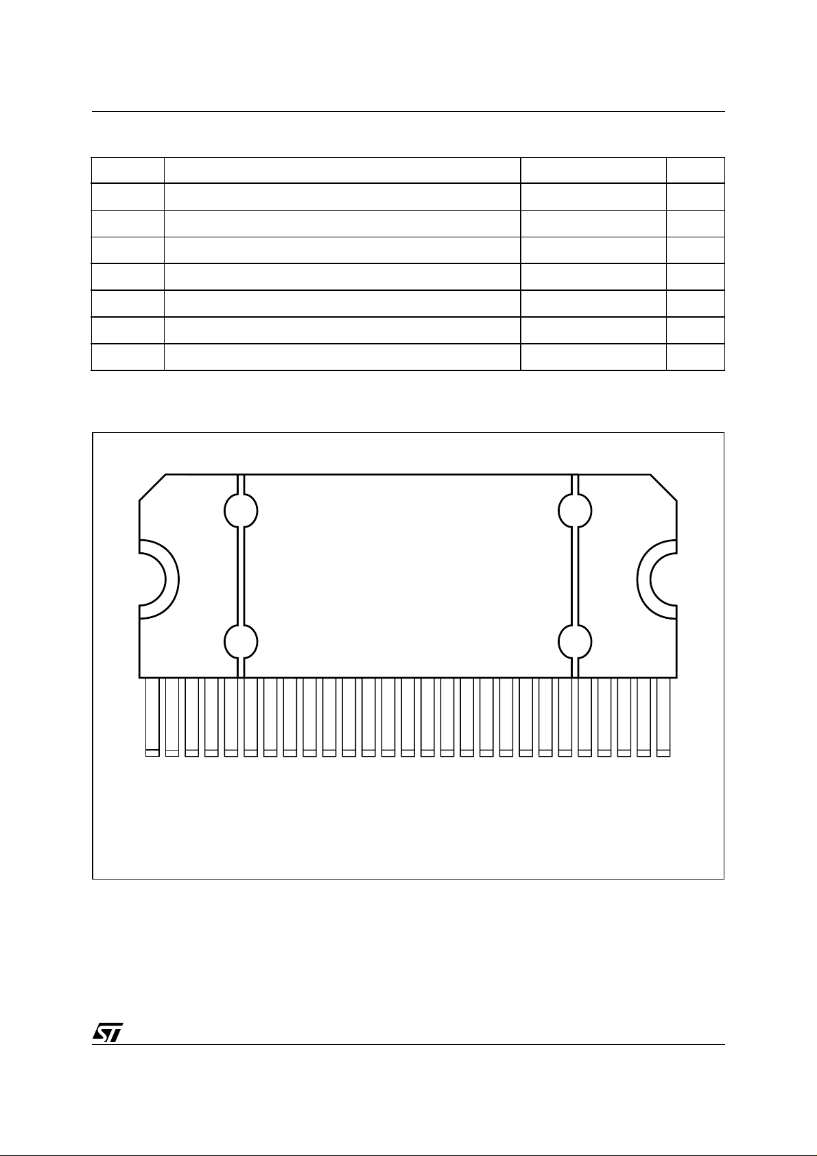
PIN CONNECTION
1
-Vs
Out1+
Out1-
CD-1&2
CD+1&2
Out2-
Out2+
NOTE
Slug connected to PINs No. 1 & 27
TRK_1
PWR_Inp2
PWR_Inp1
TRK_2/Par1&2
Gnd
TRK_Out
STBY/MUTE
+Vs
PROT
PWR_Inp3
TRK_3
PWR_Inp4
TRK_4/Par3&4
Out4+
Out4-
CD-3&4
CD+3&4
D02AU1352
Out3-
27
-Vs
Out3+
3/17
Page 4

STA530
PIN CONNECTION
N° Name Description
1 -Vs Negative Bias Supply
2 Out1+ Channel 1 speaker positive output
3 Out1- Channel 1 speaker negative output
4 CD+1&2 Channels 1 & 2 Time varying tracking rail positive power supply
5 CD-1&2 Channels 1 &2 Time varying tracking rail negative power supply
6 Out2- Channel 2 speaker negative output
7 Out2+ Channel 2 speaker positive output
8 TRK_2/
Par1&2
9 TRK_1 Absolute value block input for channel 1
10 PWR_Inp2 Input to channel 2 power stage
11 PWR_Inp1 Input to channel 1 power stage
12 STBY/MUTE Standby/mute input voltage control
13 TRK_Out Absolute value block output
14 Gnd Analog Ground
15 +Vs Positive Bias Supply
16 PROT Channel Protection signal for STABP01
17 PWR_Inp3 Input to channel 3 power stage
18 PWR_Inp4 Input to channel 4 power stage
19 TRK_3 Absolute value block input for channel 3
20 TRK_4/
Par3&4
21 Out4+ Channel 4 speaker positive output
22 Out4- Channel 4 speaker negative output
Absolute value block input for channel 2,and parallel command for channels 1&2
Absolute value block input for channel 4,and parallel command for channels 3&4
23 CD-3&4 Channels 3 & 4 Time varying tracking rail negative power supply
24 CD+3&4 Channels 3 & 4 Time varying tracking rail positive power supply
25 Out3- Channel 3 speaker negative output
26 Out3+ Channel 3 speaker positive output
27 -Vs Negative Bias Supply
4/17
Page 5

STA530
ELECTRI CAL CH ARAC TER ISTC S
Ω
8
, external components at the nominal value f = 1KHz, Tamb = 25°C unless otherwise specified)
(Test Condition: Vs+ = 25V, Vs- = -25V, V
= 15V, V
CD+
= -15V, RL =
CD-
Symbol Parameter Test Condition Min. Typ. Max. Unit
TRACKING PARAM ETER S
G
V
TRK_out
I
TRK_out
Z
TRK_in
V
OFFSET
Tracking reference voltage gain 66 70 74
TRK
Tracking ref. output voltage 0 15 V
Current capability 5 6 mA
Input impedance (T
)1MΩ
RK1/2
Output traking DC offset 100 mV
OUTPUT BRIDGE
G
G
∆G
P
Half Output bridge gain 19 20 21 dB
out
Output bridge differential gain 25 26 27 dB
ch
Output bridges gain mismatch -1 1 dB
ch
Continuous Output Power THD = 1% 39 W
out
THD = 10% 50 W
THD = 10% R
V
= 11V, V
CD+
L
CD-
= 4
Ω
= -11V
40 W
P
2 ch par
THD Total harmonic distortion of the
Continuous Output Power
out
THD = 1% R
THD = 10% R
= 4Ω
L
= 4
L
Ω
78 W
100 W
Po = 5W 0.01 0.1 %
output bridge
f = 20Hz to 20KHz; Po = 20W 0.2 %
V
Z
R
R
dsonMAX
OLG
Output bridge D.C. offset -100 100 mV
Off
EN
Noise at Output bridge pins f = 20Hz to 20KHz; Rg = 50Ω 60 µV
Input impedance 100 140 180 KΩ
br_in
Output power Rdson
dson
= 1A Tj=25o C
I
O
400 500 mΩ
Maximum Output power Rdson IO = 1A 800 mΩ
Open Loop Voltage Gain 100 dB
GB Unity Gain Bandwidth 6 MHz
SR Slew Rate 8V/µs
PROTECTION
V
V
MUTE
STBY
Stby voltage range 0 0.8 V
Mute voltage range 1.6 2.5 V
V
PLAY
T
h1
Play voltage range 4 5 V
First Over temperature threshold 130 °C
5/17
Page 6
STA530
ELECTRICAL CHARACTERISTCS
(continued)
Symbol Parameter Test Condition Min. Typ. Max. Unit
T
Second Over temperature
h2
150 °C
threshold
Unbal.
Ground
Unbal.
Ground
UV
th
P
d_reg.
Upper Unbalancing ground
threshold
Lower Unbalancing ground
threshold
Referred to (CD
Referred to (CD
Under voltage threshold |Vs+| + |Vs-| 18 22 V
Power dissipation threshold for
I
= 50µA; @ Vds = 8V 18 20 23 W
prot
+
- CD-)/2
+
- CD-)/2
5V
-5 V
system regulation
P
d_max
Switch off power dissipation
@ Vds = 8V 30 W
threshold
I
prot Pd
I
prot Id
I
I
I+Vs Positive supply current Stby (Vstby/mute pin = 0V)
Protection current slope for Pd > Pd
Protection current slope for Id > Id
Limiting Current threshold “soft” 4 4.5 5 A
lct s
Limiting Current threshold “hard” 4.5 5 5.5 A
lct h
reg
reg
400 µA/W
400 µA/A
5
Mute (Vstby/mute pin = 2.5V)
Play (Vstby/mute pin = 5V no signal)
TBD
TBD
mA
mA
mA
I-Vs Negative supply current Stby (Vstby/mute pin = 0V)
Mute (Vstby/mute pin = 2.5V)
Play (Vstby/mute pin = 5V no signal)
ICD+ Positive traking rail supply current Stby (Vstby/mute pin = 0V)
Mute (Vstby/mute pin = 2.5V)
Play (Vstby/mute pin = 5V no signal)
ICD- Negative traking rail supply current Stby (Vstby/mute pin = 0V)
Mute (Vstby/mute pin = 2.5V)
Play (Vstby/mute pin = 5V no signal)
6
29
33
200
85
85
200
85
85
mA
mA
mA
µA
mA
mA
µA
mA
mA
6/17
Page 7

STA530
FUNCTIONAL DESCRIPTION
The circuit contains all the blocks to build a configurable four channel amplifier.
In fact, only driving properly the TRK_2 (and TRK_4) pins, it’s possible to change the chip configuration:
– 50 Watt x 4
– 50 Watt x 2 + 100 Watt x1 (TRK_2/Par1&2 or TRK_4/Par3&4 at -Vs)
– 100 Watt x 2 (TRK_2/Par1&2 and TRK_4/Par3&4 at -Vs)
Each single channel is based on the Output Bridge Power Amplifier, and its protection circuit. Moreover, a signal rectifier are added to complete the circuit.
The operation modes are driven by The Turn-on/off sequence block. In fact the IC can be set in three states by
the Stby/mute pin:
STANDBY ( V
< 0.8V), MUTE (1.6V < V
pin
In the Standby mode all the circuits involved in the signal path are uninhabited, instead
in Mute mode the circuits are biased but the Speakers Outputs are forced to ground potential.
These voltages can be get by the external RC network connected to Stby/Mute pin.
The same block is used to force quickly the I.C. In standby mode or in mute mode when the I.C. dangerous
condition has been detected. The RC network in these cases is used to delay the Normal operation restore.
The protection of the I.C. are implemented by the Over Temperature, Unbalance Ground, Output Short circuit,
Under voltage, and output transistor Power sensing as shown in the following table:
< 2.5V), and PLAY (V
pin
> 4V).
pin
Table 1. Protection Implementation
Fault Type Condition Protection strategy Action time Release time
Chip Over
temperature
Chip Over
temperature
Unbalancing
Ground
Over Current Iout > 4.5A Reducing Buck
Short circuit Iout > 5A Standby Fast Slow, related to
Under Voltage |Vs+| + |Vs-|< 20V Standby Fast Slow, related to
Extra power
dissipation
at output transistor
Maximum power
dissipation
at output transistor
Tj > 130 °C Mute Fast Slow Related to
Tj > 150 °C Standby Fast Slow, Related to
|Vgnd| > ((CD+) (CD-))/2 + 5V
Pd tr. > 18W Reducing Buck
Pd tr. > 30W Standby Fast Slow, related to
Standby Fast Slow, Related to
regulator output
voltage.
regulator output
voltage.
Related to the Buck
regulator
Related to the Buck
regulator
Turn_on sequence
Turn_on sequence
Turn_on sequence
Related to the Buck
regulator
Turn_on sequence
Turn_on sequence
Related to the Buck
regulator
Turn_on sequence
ABSOLUTE VALUE BLOCK
The absolute value block rectifies the signal to extract the control voltage for the external Buck regulator. The
output voltage swing is internally limited, the gain is internally fixed to 70.
The input impedance of the rectifier is very high , to allow the appropriate filtering of the audio signal before the
rectification.
7/17
Page 8

STA530
OUTPUT BRIDGE
The Output bridge amplifier makes the single-ended to Differential conversion of the Audio signal using two
power amplifiers, one in non-invert ing configuration with gain equal to 10 and the other in inverting confi guration
with unity gain. To guarantee the high input impedance at the input pins, PWR_Inp1....4, the second amplifier
stages are driven by the output of the first stages respectively.
In 60W x2 channel configuration the "slave" inputs (INPUT 2/4) must be connected to GND.
POWER PROTECTION
To protect the output transistors of the power bridge a power detector is implemented (fig 1).
The current flowing in the power bridge and the voltage drop on the relevant power (Vds) are internally mea-
sured. These two parameters are converted in current and multiplied: the resulting current , Ipd, is proportional
to the instantaneous dissipated power on the relevant output transistor. The current Ipd is compared with the
reference current Ipda, if bigger (dis sipated pow er > 18W) a current, Iprot(P
The aim of the current Iprot is to reduce the reference voltage for the Buck regulator supplying the power stage
of the chip, and than to reduce the dissipated power. The response time of the system must be less than
µ
200
Sec to have an effective protection. As fur ther protection, when Ipd reaches an higher thr eshold (when the
dissipated value is higher then 30W) the chip is shut down, forcing low the Stby/Mute pin, and the turn on sequence is restarted. The above description is relative for each channel in 4x30W configuration.
Figure 1. Power Protection Block Diagram
), is supplied to the Protecti on pin.
D
OPA
R
SENSE
OUT1p
+
ILIMP
V/I
MULTIPLIER
I_Pd
V/I
CD+1&2
OUT1n
Iload
D02AU1346
I_pda
x
OPA
I_pd
I_pdp
I
PROT(PD)
I_pd
Ilim
CD-1&2
I
+
PROT(ID)
I
PROT
CURRENT
COMP.
Pdp1
CURRENT
COMP.
Oc1
TO PROT
PAD
SEQUENCE
TO TURN-ON/OFF
SEQUENCE
TO TURN-ON/OFF
8/17
Page 9

STA530
I
prot IL
()
I
LOADIict s
,
)
–
(
2500
--------------------------------------- -
≡
In fig. 2 there is the power protection strategy pictures. Under the curve of the 18W power, the chip is
in normal operation, over 30W the chip is forced in
Standby. This last status would be reached if the
Buck regulator does not respond quikly enough reducing the stress to less than 30W.
The fig.3 gives the protection current, Iprot(P
), be-
D
havior. The current sourced by the pin Prot follows
the formula:
–
I
()
prot PD
)–(
PdP
------------------------------------------------------------------ -
≡
d_av_th
⋅⋅
1.25V
510
4
(for each channel)
for P
< P
d
the Iprot(PD)= 0.
d_av_th
Figure 2. Powe r prot ection thresh ol d
5.0
4.5
4.0
3.5
3.0
2.5
2.0
1.5
1.0
Ids(A)
Normal
Operation
Ilim=4.5A
Standby
B
u
Pd_Max=30W
c
k
L
i
m
i
t
a
t
i
o
n
7.50
15.0 22.5 30.0 37.5
Pd_reg=18W
D02AU1366
Vds(V)
CURRENT PROTECTION
The chip is also protected by a current detection.
The current I
current I
rot(I
LIMP
), is supplied to the Protection pin.
L
As further protection, when I
is compared with the reference
LOAD
, if bigger (I
> 4,5 A)a current Ip-
LOAD
reaches an higher
LOAD
threshold (5 A) the chip is shut down, forcing low the
Stby/Mute pin, and the turn on sequence is restarted.
The above description is relative for each channel in
4x30W configuration.
The fig.4 gives the protection current, Iprot(I
), be-
L
havior. The current sourced by the pin Prot follows
the formula:
(for each channel)
< I
for I
lLOAD
the Iprot(IL) = 0.
ict,s
For the parallel channel Iprot is double.
The chip is also shut down in the following conditions:
When the average junction temperature of the chip
reaches 150°C.
When the ground potential differ from more than 5V
from the half of the power supply voltage, ((CD+)(CD-))/2
When the sum of the supply voltage
Vs+
|Vs-|
|
| +
<20V
The output bridge is muted when the average junc-
tion temperature reaches 130°C.
Figure 3. Protection current behaviour Iprot (
Iprot (IPd) (mA)
20
10
5101520
Iprot slope = 0.4 mA/W
:
25
Pd (W)
30
Figure 4. Protection current behaviour Iprot (IL)
P
)
D
Iprot(IL)(µA)
800
400
D02AU1367
1
Iprot slope=400µA/A
4.5A
23456
5A
Id(A)
9/17
Page 10

STA530
Figure 5. Tes t an d A pplication Ci rcui t (4x 5 0W )
INPUT 1
INPUT 3
C13
C14
C9
R5
R1
C5
C1
R13
R14
D1
C12
R4
R8
C8
C4
TRK_1
R9
PWR_INP1
CD+1&2
CD+3&4
+V
C17
C15
R15
R16 PROT
GND
C18C16
-V
-V
CD-1&2
CD-3&4
TRK_OUT
TRK_3
R12
PWR_INP3
TRK_2/PAR1&2
R11
PWR_INP2
OUT1P
OUT1M
S
S
S
OUT2P
OUT2M
STBY/MUTE
OUT3P
OUT3M
OUT4P
OUT4M
TRK_4/PAR3&4
PWR_INP4
D02AU1347
8Ω
8Ω
8Ω
8Ω
R10
C11
R3
R7
C7
C3
R18
C19
C10
R6
R2
C6
C2
MUTE
R19
INPUT 2
R17
STBY
INPUT 4
5V
Figure 6. Test and Application Circuit (2x50W & 1x100W)
C9
INPUT 1
INPUT 3
C13
C14
R5
R1
C5
C1
R13
R14
D1
C12
R4
R8
C8
C4
TRK_1
R9
PWR_INP1
CD+1&2
CD+3&4
+V
C17
C15
R15
R16 PROT
GND
C18C16
-V
-V
CD-1&2
CD-3&4
TRK_OUT
TRK_3
R12
PWR_INP3
S
S
S
TRK_2/PAR1&2
PWR_INP2
OUT1P
OUT2P
OUT2M
OUT1M
STBY/MUTE
OUT3P
OUT3M
OUT4P
OUT4M
TRK_4/PAR3&4
R10
PWR_INP4
D02AU1351
-V
S
4Ω
R18
C19
MUTE
8Ω
8Ω
R6
R2
C2
R19
C10
INPUT 4
C6
R17
STBY
5V
10/17
Page 11

EXTER NA L COM P ON EN T S
Name Function Value Formula
R1 = R2 =R7 = R8
R5 = R6 =R3 = R4
Cac
C1 = C2 = C3 = C4
R9=R10=R11=R12
C5 = C6 = C7 = C8 Capacitor for Tracking input
C9=C10=C11=C12 Dc decoupling capacitor 1µF
R17
R18 Stby/Mute constant time resistor 30KΩ
R19 M ute resisto r 30KΩ
C19 Capacitor for Stby/Mute resistor 2.2µF
C17 = C18 Power supply filter capacitor 100nF
R13 = R14 Centering resistor 330 Ω, 1W
C13 = C14 Tracking rail power supply filter 680nF
R15 TRK_out 40KΩ
R16 Protection 1KΩ
C15 = C16 Power supply filter capacitor 470 µF , 63V
D1 Schottky diode SB360
Resistor for tracking input voltage
filter 10KΩ
Resistor for tracking input voltage
filter 56KΩ
AC Decoupling capacitor 100nF
(fp = 16Hz,
Rac =100KΩ )
Resistor for tracking input voltage filter
10KΩ
1nF
voltage filter
Bias Resistor for Stby/Mute function
10KΩ
Cac
STA530
1
-------------------------------- -=
2π fp Rac⋅⋅
Figure 7. BASH® module SAM261 6.1 with 2 x STA530
Signal Power Supply
+50VDC
+50VDC
Dynamic Power Supply
Dynamic Power Supply
(CD+ & CD-)
Buck
Buck
Regulator
Regulator
STABP01
STABP01
Controller
Controller
BASH fi module SAM261 6.1
BASH fi module SAM261 6.1
(CD+ & CD-)
Lines of Controls
Lines of Controls
Signal Power Supply
+/-24V DC / 50 mA
+/-24V DC / 50 mA
(see Application Note AN1643)
STA530
STA530
4 x 50Watts
4 x 50Watts
AudioInputs
AudioInputs
STA530
STA530
1 x 100Watts
1 x 100Watts
2 x 50Watts
2 x 50Watts
+/-24V DC / 50 mA
+/-24V DC / 50 mA
Signal Power Supply
Signal Power Supply
8 Ohm Loads
8 Ohm Loads
4 Ohm Load
4 Ohm Load
Power - On-Off sequences:
In order to avoid damages to the SAM261 board it is important to follow these sequences:
Power-On
At
(+50V)
, in this condition the system is in "Mute state" and it can move in "play state" with the switch present
apply in the first the
Auxiliary Power Supply (±24V)
and after the
Main Power Supply
on the pcb.
Power-Off
At
off the
is better to bring the SAM module in "Mute state" and after that to follow this order: switch-
Main Supply Voltage (+50V)
and subsequently the
Auxiliary Power Supply. (±24V)
.
11/17
Page 12

STA530
System Description & Operating Rules
SAM261 is a BASH® 6.1 amplifier ( 6 x 50W, 1 x 100W) implementation utiliz ing the STA530 Integrated Circuit.
Specifically designed for multi-channel implementation in DVD - HTIB systems, Multi-Media systems, Mini and
Micro systems and Set Top boxes.
SAM261 is dimensioned to provide the maximum Output Power (THD=10 %) on two channels and instantaneously and 1/3 max Pout on the remaining Outputs, or 1/8 of max Pout continuous; this rule is important to
define the main Power Supply size (+50V).
Buck Regulator Description
The function of the buck regulator is to effi cient conv er t efficientl y an input voltage to a low er voltage by a djusting the ratio of the switching transistor's on-time to off-time. The resulting waveform is averaged by the output
filter to recover an analog signal.
In the BASH amplifier this output is in effect split in half by centering it on the audio ground to provide CD+ and
CD- rails.
To avoid the need for a high side driver for the transistor switch in the buck regulator the buck circuit recommended has the switch in the return path. Hence the gate driv e circuit (par t of the STPB01) is refer enced to the
negative return of the main supply that provides power for the buck regulator.
Interfacing STA530 to STPB01 (Feedback circuit)
This circuit produces a control signal current that is fed back to the STPB01 digital controller. The network used
in this example compares the track signal (STA530 track out) to a fixed ratio of buck regulator's output (CD+)
using a transistor. This method is effective because the controller's reference is the negative of the main DC
supply, which is not referenced to audio ground.
The tracking signal is generated inside the STA530 (track out) by taking the absolute value of the pre-amp's
output. The outputs of each channel and of each STA530 are then tied together in a diode-oring arrangement.
This means that the highest of any given output is the output that determines the tracking signal.
The absolute value circuit inside the STA530 has gain. This makes it possible to use an RC network and a resistor divider to create a phase shift in the tracking signal at higher frequencies. This is also useful i n optimiz ing
the alignment of the buck regulator's output with the output signal of the bridge amplifier at high frequency
This circuit first converts the buck switch current to a peak voltage. The control current is then converted to a
voltage (using a resistor ) and added to the peak voltage. By doing this, the buck is better able to maintain the
desired headroom over a wide load range and output level.
Centering Network for CD + & C D- Rails
The power rail of a bridge amplifier has no current flowi ng through the ground node, as the load is not connected
to ground. However there are sev eral differ ent small sources of dynam ic and continuos ground currents flowing
from either CD+ or CD- to s upport the fu nction of various things such as the control signal to the STABP01 controller. The centering network prevents these currents from shifting the CD+/- rails away from center i.e. away
from a symmetric split of the buck's output about ground. This is critical, even a small centering error requires
an increase in headroom which results in a significant drop in output losses. In its simplest form the centering
network could be a resistor divider from CD+ to CD- with its center tied to ground. As long as the impedance is
low enough (for example 200
Ω
) this will swamp the small er offset currents. It i s helpful to put this ki nd of passive
network on the board with the STA530 devices to help when testing this board on its own.
Power Amplifier Heatsink requirements
The heatsink requir ements are dependent on sev eral design goals. However there are tw o common references:
Pink noise at 1/8 of full power, all channels loaded. This would approximate a system with all channels reproducing music at full volume with clipping occurring only occasionally. The second would be full power at 1kHz
for 5 minutes after a one hour pre-soak at 1/8 power.
The worse of these two is the full power test. A conservative approach is to assume that the heatsink would
come to thermal equilibrium after 5 minutes. Thus the Rth of the heatsink can be determined by:
12/17
Page 13

STA530
T
–
R
For example in the STA530 the Rth jc is 1°C/W. R case-to-heatsink with grease is about 0.5 °C/W. The maximum operating junction temperature is 130 °C, which for margin should be derated to 120 °C.
Buck Regulator Heatsink
The Buck regulator heatsink ca n be designed in a simi lar manner and does not change by var ying power supply.
In general the efficiency will be in the or der of 85%. The thermal impedances fr om the junction(s) to the heatsi nk
may be lower and the maximum operating temperature will be higher. Usually either the sub or the remaining
channels are tested at full power. The result is that usually the Buck heatsink is about ¼ the size of the linear
heatsink, but this can be strongly affected by the design.
Figure 8. PCBs AND COMPONENTS LAYOUT
Main DC
Input
VS DC
Input
Mute
Audio
Inputs
Preamplifier PCB
jmaxTamb
---------------------------------- R
th
–
P
d
4 Supply Connections
th j case
4 Pins Harness
Power Supply Connections
9 Pins Harness
Audio Connections
R
––=
th c a s e t o heatsink
Amplifier PCB
SAM261 Specification
Parameter Rating Notes
Output Power Sats @ 8Ω - 55 Watts @ 10%
Sub @ 4Ω - 100 Watts @ 10%
THD + N < 0.05% @ 40 Watts
< 0.05% @ 75 Watts
SNR -102 dB (relative to full power)
-110 dB (A-weighted)
Sensitivity 1 VRMS Amplifier
Crosstalk -87dB (relative to10W) Channel 5 @ 10W 1KHz 8Ω,
Main Power Supply Inputs 50Volts @ 2 Amps Maximum Voltage is 50Vdc
Aux Power Supply Inputs + 24 Volts @ 100mA
-24 Volts @ 100mA
See Graphs
Measured @ 1KHZ
Channel 5 terminate d
Channel 3 input terminated
Minimum Voltage is 40Vdc
13/17
Page 14

STA530
k
k
Figure 9. THD + N FR Channel
Audio P recis ion
Audio P recis ion
10
10
5
5
2
2
1
1
0.5
0.5
%
%
0.2
0.2
0.1
0.1
0.05
0.05
0.02
0.02
0.01
0.01
2.5 605 7.5 10 12.5 15 17.5 20 22.5 25 27.5 30 32.5 35 37.5 40 42.5 45 47.5 50 52.5 55 57.5
2.5 605 7.5 10 12.5 15 17.5 20 22.5 25 27.5 30 32.5 35 37.5 40 42.5 45 47.5 50 52.5 55 57.5
W
W
Figure 10. THD + N vs Frequency
Audio Precision
Audio Precision
Audio Precision
10
10
10
5
5
5
2
2
2
1
1
1
0.5
0.5
0.5
%
%
%
0.2
0.2
0.2
0.1
0.1
0.1
0.05
0.05
0.05
0.02
0.02
0.02
0.01
0.01
0.01
20 20k50 100 200 500 1k 2k 5k 10k
20 20k50 100 200 500 1k 2k 5k 10k
20 20k50 100 200 500 1k 2k 5k 10k
Pout = 30W
Pout = 30W
Pout = 5W
Pout = 5W
Hz
Hz
Hz
Figure 12. THD + N LF Channel
Audio P re cisio n
Audio P re cisio n
10
10
5
5
2
2
1
1
0.5
0.5
%
%
0.2
0.2
0.1
0.1
0.05
0.05
0.02
0.02
0.01
0.01
5 12010 15 20 25 30 35 40 45 50 55 60 65 70 75 80 85 90 95 100 105 110 115
5 12010 15 20 25 30 35 40 45 50 55 60 65 70 75 80 85 90 95 100 105 110 115
W
W
Figure 13. Frequency Response
Audio Precision
Audio Precision
+30
+30
+29
+29
+28
+28
+27
+27
+26
+26
+25
+25
+24
+24
+23
+23
+22
+22
+21
+21
+20
+20
+19
+19
+18
+18
+17
+17
+16
+16
+15
+15
dBr
dBr
+14
+14
+13
+13
+12
+12
+11
+11
+10
+10
+9
+9
+8
+8
+7
+7
+6
+6
+5
+5
+4
+4
+3
+3
+2
+2
+1
+1
+0
+0
20 50 100 200 500 1k 2k 5k 10k 20k
20 50 100 200 500 1k 2k 5k 10k 20k
10 40
10 40
Hz
Hz
Figure 11. Residual Noise vs Freq - Relative to
full power
Audio P re cision
Audio P re cision
+0
+0
-10
-10
-20
-20
-30
-30
-40
-40
-50
-50
-60
-60
-70
-70
-80
-80
dBr
dBr
-90
-90
-100
-100
-110
-110
-120
-120
-130
-130
-140
-140
-150
-150
-160
-160
20 20k50 100 200 500 1k 2k 5k 10k
20 20k50 100 200 500 1k 2k 5k 10k
14/17
Hz
Hz
Page 15

Figure 14. Application Block Diagram
+V
-V
S
S
STA530
4 CHANNELS
STA530
S1
1800pF
DC++
1800pF
+V
S
-V
S
MUTE
MUTE CONTROL
MUTE-BUCK
+V
S
-V
S
+V
S
-V
MUTE-BUCK
S
DC++
GATE-DRIVE
BUCK CONTROLLER
I-SENSE
MUTE
TRACK
PROT
CDCD+
J1
CONNECTOR
J2
CONNECTOR
MUTE
RED
WHITE
RED
WHITE
IN1
IN2
IN3
IN4
CD-
CD+
50W
50W
50W
50W
OUT1+
OUT1-
OUT2+
OUT2-
OUT3+
OUT3-
OUT4+
OUT4TRACK
PROT
J1
J2
J3
J4
I-SENSE
L3
15µH
GATE-DRIVE
DC++
200W BUCK
CD+
CD-
-V
S
+V
S
D02AU1444
CD+
CD-
MUTE
-V
J3
+V
IN5
RED
IN6
WHITE
J4
IN7
S
S
STA530
3 CHANNELS
50W
50W
100W
PROT
TRACK
OUT5+
OUT5-
OUT6+
OUT6-
OUT7+
OUT7-
J5
J6
J7
15/17
Page 16

STA530
DIM.
MIN. TYP. MAX. MIN. TYP. MAX.
mm inch
A 4.45 4.50 4.65 0.175 0.177 0.183
B 1.80 1.90 2.00 0.070 0.074 0.079
C 1.40 0.055
D 0.75 0.90 1.05 0.029 0.035 0.041
E 0.37 0.39 0.42 0.014 0.015 0.016
F (1) 0.57 0.022
G 0.80 1.00 1.20 0.031 0.040 0.047
G1 25.75 26.00 26.25 1.014 1.023 1.033
H (2) 28.90 29.23 29.30 1.139 1.150 1.153
H1 17.00 0.669
H2 12.80 0.503
H3 0.80 0.031
L (2) 22.07 22.47 22.87 0.869 0.884 0.904
L1 18.57 18.97 19.37 0.731 0.747 0.762
L2 (2) 15.50 15.70 15.90 0.610 0.618 0.626
L3 7.70 7.85 7.95 0.303 0.309 0.313
L4 5 0.197
L5 3.5 0.138
M 3.70 4.00 4.30 0.145 0.157 0.169
M1 3.60 4.00 4.40 0.142 0.157 0.173
N 2.20 0.086
O 2 0.079
R 1.70 0.067
R1 0.5 0.02
R2 0.3 0.12
R3 1.25 0.049
R4 0.50 0.019
V 5˚ (Typ.)
V1 3˚ (Ty p.)
V2 20˚ (Typ.)
V3 45˚ (Typ.)
(1): dam-bar protusio n not included
(2): molding protusion i ncluded
OUTLINE AND
MECHANICAL DA T A
Flexiwatt27 (vertical)
16/17
L2
V
C
B
H
V3
H3
OL3 L4
Pin 1
G
H1
G1
H2
R3
R4
N
V2
F
V
A
V1
R2
R
L
L1
V1
R2
FLEX27ME
L5
R1
R1 R1
M
D
E
M1
7139011
Page 17

STA530
Information furnished is believed to be accurate and reliable. However, STMicroelectronics assumes no responsibility for the consequences
of use of such information nor for any infringement of patents or other rights of third parties which may result from its use. No license is granted
by implic ation or oth erwise under any patent or patent rights of STMicroe l ectronics. Specificat i ons mentioned in this publicati on are subject
to change without notice. This publication supersedes and replaces all information previously supplied. STMicroelectronics products are not
authorized for use as critical comp onents in life su pport device s or systems without expres s written approval of STMi croelectro nics.
The ST logo is a registered trademark of STMicroelectronics
2003 STMi croelectr oni cs - All Righ ts Reserved
Australi a - Brazil - Canada - China - F i nl and - France - Germany - Hong Kong - Ind ia - Is rael - Italy - Japan - Malaysia - Malt a - Morocco -
Singap ore - Spain - Sw eden - Switze rl and - United K i ngdom - Unit ed States.
STMicroelectronics GROUP OF COMPANIES
http://www.s t. com
17/17
 Loading...