

Page 1
30V 3.5A QUAD POWER HALF BRIDGE
■ MINIMUM INPUT OUTPUT PULSE WIDTH
DISTORTION
■ 200mΩ R
OUTPUT STA GE
■ CMOS COMPATIBLE LOGIC INPUTS
■ THERMAL PROTECT I O N
■ THERMAL WARNING OUTPUT
■ OVERVOLTAGE, UNDERVOLTAGE
PROTECTION
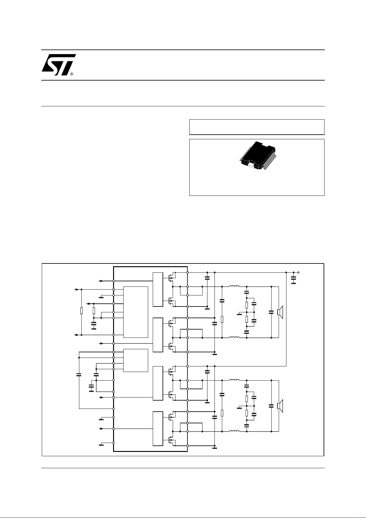
DESCRIPTION
STA500 is a monoli thic quad half bridge stage in Multipower BCD Technology. The device can be us ed as
dual bridge or reconfigured, by connecting CONFIG
pin to Vdd pin, as single bridge with double current
capability, and as half bridge (Binary mode) with half
COMPLEMENTAR Y DM OS
dsON
STA500
MULTIPOWER BCD TECHNOLOGY
PowerSO36
ORDERING NUMBER: STA500
current capability.
The device is particulary de signed to mak e the output
stage of a stereo All-Digital High Efficiency (DDX™)
amplifier capable to deliver 30 + 30W output power
on 8
Ω
load and 60W on 8Ω load in bridge BTL con-
Ω
figuration or mono 60W on 4
have threshold proportional to Ibias pin voltage.
load. The input pins
AUDIO APPLICATION CIRCUIT (Dual BTL)
29
IN1A
+3.3V
TH_WAR
100nF
C58
R57
10K
C58
100nF
C60
100nF
R59
10K
C53
100nF
IN1A
TRI-STATE
IN1B
IN2A
GND-Clean
IN2B
IBIAS
CONFIG
PWRDNPWRDN
FAULT
TH_WAR
IN1B
V
V
V
V
VCCSIGN
V
SIGN
CC
IN2A
GND-Reg
IN2B 32
GNDSUB
DD
DD
SS
SS
23
24
25
27
26
28
30
21
22
33
34
35
36
31
20
19
1
PROTECTIONS
&
LOGIC
REGULATORS
M17
M15
M16
M14
1A
V
CC
15
M3
M2
M5
M4
C30
1µF
17
OUT1A
16
OUT1A
14
GND1A
12
V
1B
CC
OUT1B
OUT1B
GND1B
2A
V
CC
OUT2A
OUT2A
GND2A
V
2B
CC
OUT2B
OUT2B
GND2B
C32
1µF
C31
1µF
C33
1µF
11
10
13
7
8
9
6
4
3
2
5
L18 22µH
C52
330pF
R63
20
L19 22µH
L113 22µH
C109
330pF
R104
20
L112 22µH
D00AU1148B
C20
100nF
R98
6
R100
6
C21
100nF
C110
100nF
R103
6
R102
6
C111
100nF
C99
100nF
C23
470nF
C101
100nF
C107
100nF
C108
470nF
C106
100nF
+V
CC
C55
1000µF
July 2003
1/10
Page 2
STA500
PIN FUNCTION
N° Pin Description
1 GND-SUB Substrate ground
35 ; 36 Vcc Sign Signal Positive supply
15 Vcc1A Positive Supply
12 Vcc1B Positive Supply
7 Vcc2A Positive Supply
4 Vcc2B Positive Supply
14 GND1A Negative Supply
13 GND1B Negative Supply
6 GND2A Negative Supply
5 GND2B Negative Supply
16 ; 17 OUT1A Output half bridge 1A
10 ; 11 OUT1B Output half bridge 1B
8 ; 9 OUT2A Output half bridge 2A
2 ; 3 OUT2B Output half bridge 2B
29 IN1A Input of half bridge 1A
30 IN1B Input of half bridge 1B
31 IN2A Input of half bridge 2A
32 IN2B Input of half bridge 2B
21 ; 22 Vdd 5V Regulator referred to ground
33 ; 34 Vss 5V Regulator referred to +Vcc
25 PWRDN Stand-by pin (Control input)
26 TRI-STATE Hi-Z pin (Control input)
27 FAULT Fault pin advisor (Open Collector Output)
24 CONFIG Configuration setting pin
28 TH-WAR Thermal warning advisor (Open Collector Output)
19 GND-clean Logical ground
23 IBIAS High logical state setting voltage
18 NC Not connected
20 GND-Reg Ground for Vdd regulator
2/10
Page 3
FUNCTIONAL PIN STATUS
PIN NAME Logical value IC -STATUS
STA500
FAULT 0 Fault detected (Short circuit, or
FAULT
(*)
1 Normal Operati on
TRI-STATE 0 All powers in Hi-Z state
TRI-STATE 1 Normal operati on
PWRDN 0 Low absorpion
PWRDN 1 Normal operati on
THWAR 0 Temperature of the IC =130°C
THWAR
(*)
1 Normal operati on
CONFIG 0 Normal Operation
CONFIG
(*) : The pin is open collector. To have the high logic va l ue, it needs to be pulled up by a r esistor.
(**:) To put CONFIG = 1 mean s connect Pin 24 (CONFIG) to P i ns 21, 22 (Vdd)
(**)
1 OUT1A=OUT1B ; OUT2A=OUT2B
PIN CONNECTION
Thermal ..)
(IF IN1A = IN1B; IN2A = IN2B)
GND-SUB
OUT2B
OUT2B
2B
V
CC
GND2B
GND2A IN2A
V
2A
CC
OUT2A
OUT2A TH_WAR
OUT1B
OUT1B
V
1B
CC
GND1B
GND1A
V
1A
CC
OUT1A
OUT1A GND-Reg
N.C. GND-Clean
1
2
3
4
5
6
7
8
9
10 27
11
12
13 24
14
15
16
17
18
D00AU1133
36
35
34
33
32
31
30
29
28
26
25
23
22
21
20
19
V
VCCSign
V
V
IN2B
IN1B
IN1A
FAULT
TRI-STATE
PWRDN
CONFIG
IBIAS
V
V
CC
SS
SS
DD
DD
Sign
3/10
Page 4

STA500
ABSOLUTE MAXIMUM RATINGS
Symbol Parameter Value Unit
V
CE
V
max
T
op
T
stg
THERMAL DATA
Symbol Parameter Min. Typ. Max. Unit
T
j-case
T
jSD
T
warn
t
hSD
ELECTRICAL CHARACTERISTCS
(Ibias = 3.3V; Vcc = 28V; T
Symbol Parameter Test conditions Min. Typ. Max. Unit
R
dsON
I
dss
g
N
g
P
Dt_s Low current Dead Time (static) see test circuit no.1; see fig. 1 10 20 ns
Dt_d High current Dead Time (dinamic) L=22µH; C = 470nF; Rl = 8Ω
t
d ON
t
d OFF
t
r
t
f
V
CC
V
IN-H
V
IN-L
I
IN-H
I
IN-L
I
PWRDN-H
V
L
V
H
DC Supply Voltage (Pin 4,7,12,15) 40 V
Maximum Voltage on pins (23 to 32) 5.5 V
Operating Temperature Range 0 to 70 °C
, TjStorage and Junction Temperature -40 to 150 °C
Thermal Resistance Junction to Case (thermal pad) 2.5 °C/W
Thermal shut-down junction temperature 150 °C
Thermal war ning tempe rature 130 °C
Thermal shut-d own hysteresis 25 °C
= 25°C unless otherwise specified)
amb
Power Pchannel/Nchannel
MOSFET R
dsON
Power Pchannel/Nchannel
leakage I
dss
Power Pchannel RdsON
Matching
(*)
Power Nchannel RdsON
Matching
(*)
Id=1A; 200 270 mΩ
Vcc=35V 50 µA
Id=1A 95 %
Id=1A 95 %
50 ns
Id = 3.5A; see fig. 3
Turn-on delay time Resistive load 100 ns
Turn-off delay time Resistive load 100 ns
Rise time Resistive load; as fig. 1 25 ns
Fall time Resistive load; as fig. 1 25 ns
Supply voltage operating voltage 9 V
OV
High level input voltage Ibias/2
+300mV
Low level input voltage Ibias/2
-300mV
Hi level Input current Pin voltage=Ibias 1 µA
Low level input current Pin voltage = 0.3V 1 µA
Hi level PWRDN pin input current Ibias = 3.3V 35 µA
Low logical state voltage VL (pin
Ibias = 3.3V 0.8 V
PWRDN, TRISTATE) (note 1)
High logical state voltage VH (pin
Ibias = 3.3V 1.7 V
PWRDN, TRISTATE) (note 1)
V
V
V
4/10
Page 5

STA500
ELECTRICAL CHARACTERISTCS
(Ibias = 3.3V; Vcc = 28V; T
amb
(continued)
= 25°C unless otherwise specified)
Symbol Parameter Test conditions Min. Typ. Max. Unit
I
VCC-
PWRDN
I
FAULT
Supply current from Vcc in Power
Down
Output Current pins
FAULT -TH-WARN when
PWRDN = 0 3 mA
Vpin = 3.3V 1 mA
FAULT CONDITIONS
I
VCC-hiz
Supply current from Vcc in Tri-
Tri-state=0 22 mA
state
I
VCC
I
OUT-SH
Supply current from Vcc in
operation
(both channel switching)
Overcurrent Protection Threshold
Input pulse width = 50% Duty;
Switching Frequency = 384Khz;
No LC filters;
80 mA
3.5 6 8 A
(short circuit current limit) (note 2)
V
V
t
pw_min
Notes: 1. The following table explains the VL, VH variation with Ibias
Overvoltage protection threshold 30 35 40 V
OV
Undervoltage protection threshold 7 V
UV
Output minimum pulse width No Load 70 150 ns
Ibias VLmin VHmax Unit
2.7 0.7 1.5 V
3.3 0.8 1.7 V
5 0.85 1.85 V
Note 2: If used in single BTL configuration, the device may be not short circuit protected
LOGIC TRUTH TABLE
(see fig. 2)
TRI-STATE INxA INxB Q1 Q2 Q3 Q4
0 X X OFF OFF OFF OFF Hi-Z
1 0 0 OFF OFF ON ON DUMP
1 0 1 OFF ON ON OFF NEGATIVE
1 1 0 ON OFF OFF ON POSITIVE
1 1 1 ON ON OFF OFF Not used
OUTPUT
MODE
5/10
Page 6

STA500
Figure 1. Tes t Circ ui t.
Figure 2.
Low current dead time = MAX(DTr,DTf)
Duty cycle = 50%
M58
INxY
M57
gnd
+Vcc
OUTxY
+V
OUTxY
Vcc
(3/4)Vcc
(1/2)Vcc
(1/4)Vcc
t
DTfDTr
R 8Ω
+
V67 =
-
vdc = Vcc/2
D03AU1458
CC
Q1
INxA INxB
OUTxA
Q3
GND
Q2
OUTxB
Q4
D00AU1134
Figure 3.
High Current Dead time for Bridge application = ABS(DTout(A)-DTin(A))+ABS(DTOUT(B)-DTin(B))
+V
CC
Duty cycle=A Duty cycle=B
M58
DTin(A)
INxA
M57
Duty cycle A and B: Fixed to have DC output current of 3.5A in the direction shown in figure
Q1
OUTxA
Q3
DTout(A)
Iout=3.5A
C69
470nF
Rload=8Ω
C71 470nF
Q2
DTout(B) DTin(B)
L68 22µL67 22µ
C70
470nF
OUTxB
Iout=3.5A
Q4
M64
M63
D00AU1162
INxB
6/10
Page 7

Figure 4. Typical Quad Half Bridge Configuration
STA500
+3.3V
TH_WAR
C58
100nF
R57
10K
100nF
C60
100nF
C58
100nF
R59
C53
10K
IN1A
IN1B
IN2A
IN2B
IN1A
IBIAS
CONFIG
PWRDNPWRDN
FAULT
TRI-STATE
TH_WAR
IN1B
V
V
VCCSIGN
V
SIGN
CC
IN2A
GND-Reg
GND-Clean
IN2B 32
GNDSUB
1P
V
CC
29
23
24
25
PROTECTIONS
27
26
28
30
21
DD
22
DD
V
33
SS
V
34
SS
35
36
31
20
19
1
&
LOGIC
REGULATORS
M3
M2
M5
M4
M17
M15
M16
M14
15
17
16
14
12
11
10
13
7
8
9
6
4
3
2
5
D03AU1474
OUTPL
OUTPL
PGND1P
V
1N
CC
OUTNL
OUTNL
PGND1N
2P
V
CC
OUTPR
OUTPR
PGND2P
V
2N
CC
OUTNR
OUTNR
PGND2N
C51
1µF
C52
1µF
C41
330pF
C61
100nF
C42
330pF
C43
330pF
C62
100nF
C44
330pF
R41
R42
R43
R44
L11 22µH
C71
100nF
20
R51
6
L12 22µH
C72
100nF
20
R52
6
L13 22µH
C73
100nF
20
R53
6
L14 22µH
C74
100nF
20
R54
6
C81
100nF
C82
100nF
C83
100nF
C84
100nF
R61
R62
R63
R64
R65
R66
R67
R68
C31 820µF
5K
C91
1µF
5K
C32 820µF
5K
C92
1µF
5K
C33 820µF
5K
C93
1µF
5K
C34 820µF
5K
C94
1µF
5K
+V
CC
C21
2200µF
Note:
The diagran showed below, have been obtained using the demonstration board described in the application
Note AN1456 (STA304 + STA500 Digital Audioprocessor evolution board evaluating manual - Jan 2002), refer
to the schematic shown in fig. 1).
For the Quad Half Bridge Configuration (fig. 4), refers to the application note AN1661 (STA308 Half Bridge
Board - March 2003)
7/10
Page 8

STA500
(
)
Figure 5. Disto rti on v s Output Powe r
(STA304A+STA500)
10
5
Vcc=30V
2
1
0.5
%
0.2
0.1
0.05
0.02
0.01
700m 5012345678910203040
Rl=80hm
f=1KHz
Eq
.
W
Figure 6. Tolal Power Dissipation & Efficiency
vs Output Power
90
80
Pdiss
70
60
Eff (%)
50
40
Efficiency
STA304A+STA500
1channel
Vcc=25V
Rl=8ohm
F=1KHz
30
20
0 5 10 15 20 25 30
Pout (W)
7
6
5
4
3
2
1
0
Figure 7. Out put P ower vs Supply V ol ta ge
(STA304A+STA500)
50
Pout (W)
45
40
35
30
25
20
15
10
5
0
+12 +18+12.5 +13 +13.5 +14 +14.5 +15 +15.5 +16 +16.5 +17 +17.5
STA500
4 ohm load
filter 22uH+ 0.47uF diff+
0.1uF common mode
Vdc
Vsupply (V)
Figure 8. Out put P ower vs Supply V ol ta ge
(STA304A+STA500)
50
Pout (W)
45
W
Pdiss
40
35
30
25
20
15
10
5
+12 +28+13 +14 +15 +16 +17 +18 +19 +20 +21 +22 +23 +24 +25 +26 +27
Rload = 8 ohm
f = 1KHz
THD = 10%
Vcc (V)
THD = 10%
THD = 1%
THD = 1%
8/10
Page 9

STA500
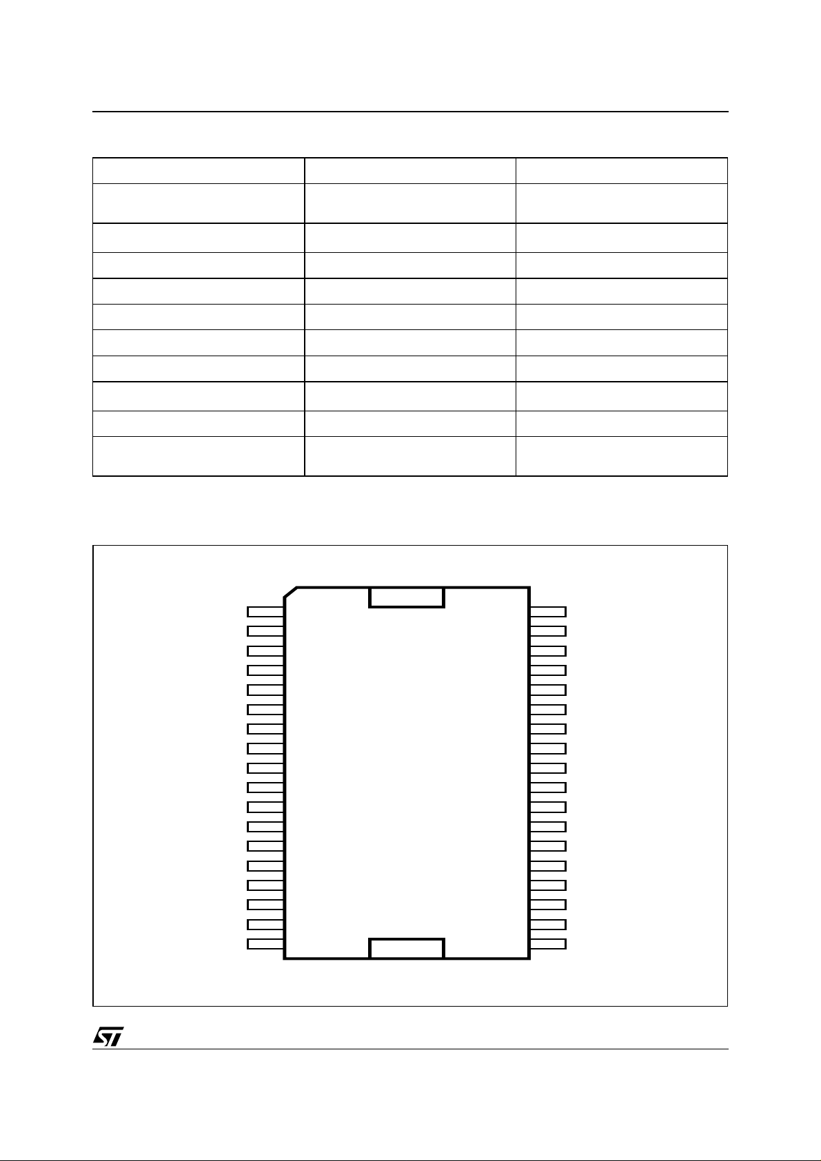
DIM.
MIN. TYP. MAX. MIN. TYP. MAX.
mm inch
A 3.60 0.141
a1 0.10 0.30 0.004 0.012
a2 3.30 0.130
a3 0 0.10 0 0.004
b 0.22 0.38 0.008 0 .015
c 0.23 0.32 0.009 0.012
D (1) 15.80 16.00 0.622 0.630
D1 9.40 9 .80 0.370 0.385
E 13.90 14.50 0.547 0.570
e 0.65 0.0256
e3 11.05 0.435
E1 (1) 10.90 11.10 0.429 0.437
E2 2.90 0.114
E3 5.80 6.20 0.228 0.244
E4 2.90 3.20 0.114 0.126
G 0 0.10 0 0.004
H 15.50 15.90 0.610 0.626
h 1.10 0.043
L 0.80 1.10 0.031 0.043
N10°(max.)
S8°(max.)
(1): "D" and "E1" do not include mold flash or protrusions
- Mold flash or protrusions shall not exceed 0.15mm (0.006 inch)
- Critical dimensions are "a3", "E" and "G".
OUTLINE AND
MECHANICAL DATA
PowerSO36
NN
a2
A
1936
0.12 AB
⊕
e
M
E1
DETAIL B
lead
a3
B
Gage Plane
PSO36MEC
BOTTOM VIEW
DETAIL B
0.35
S
E
DETAIL A
L
E2
h x 45˚
DETAIL A
118
A
e3
H
D
b
c
a1
slug
E3
D1
- C -
SEATING PLANE
GC
(COPLANARITY)
9/10
Page 10

STA500
Information furnished is believed to be accurate and reliable. However, STMicroelectronics assumes no responsibility for the consequences
of use of such information nor for any infringement of patents or other rights of third parties which may result from its use. No license is granted
by implic ation or oth erwise under any pat ent or patent rights of STMicroe l ectronics. Specificat i ons menti oned in this publicati on are subject
to change without notice. This publication supersedes and replaces all information previously supplied. STMicroelectronics product s are not
authorized for use as cri t i cal compone nt s i n l i f e support dev i ces or systems wi t hout express written approval of STMi croelectronics.
The ST logo is a registered trademark of STMicroelectronics
2003 STMicroelectronics - All Ri ghts Reserved
DDX is a trademark of Apogee tecnolo gy inc.
Austra lia - Brazil - Canada - Chi na - F i nl and - France - Germany - Hong Kong - Indi a - Israel - Italy - Japan -Ma laysia - Mal ta - Morocco -
Singap ore - Spain - Sw eden - Switze rl and - United Kingdom - U ni ted States.
STMicroelectronics GROUP OF COMPANIES
http://www.s t. com
10/10
 Loading...