

Page 1

FEATURES
■ Application specific features
• 12 channel GPS correlation DSP hardware,
ST20 CPU (for control and position
calculations) and memory on one chip
• no TCXO required
• RTCA-SC159 / WAAS / EGNOS supported
■ GPS performance
• accuracy
- stand alone withSA on <100m, SA off <30m
- differential <1m
- surveying <1cm
• time to first fix
- autonomous start 90s
- cold start 45s
- warm start 7s
- obscuration 1s
■ Enhanced 32-bit VL-RISC CPU - C2 core
• 16/33/50 MHz processor clock
• 25 MIPS at 33 MHz
• fast integer/bit operations
■ 64 Kbytes on-chip SRAM
■ 128 Kbytes on-chip ROM
■ Programmable memory interface
• 4 separately configurable regions
• 8/16-bits wide
• support for mixed memory
• 2 cycle external access
■ Programmable UART (ASC)
■ Parallel I/O
■ Vectored interrupt subsystem
■ Diagnostic control unit
■ Power management
• low power operation
• power down modes
■ Professional toolset support
• ANSI C compiler/link driver and libraries
• Debugging/profiling and simulation tools
■ Technology
• Static clocked 50 MHz design
• 3.3 V, sub micron technology
■ 100 pin PQFP package
■ JTAG Test Access Port
ST20-GP6
GPS PROCESSOR
PRELIMINARY DATA
GPS
radio
ST20-GP6
12 channel GPS
hardware DSP
Low
power
controller
Real time
clock/calendar
Programmable
memory
interface
64K
SRAM
128K optional
mask ROM
APPLICATIONS
■ Global Positioning System (GPS) receivers
■ Car navigation systems
■ Fleet management systems
■ Time reference for telecom systems
ST20
CPU
Interrupt
controller
Serial
communications
2 UART (ASC)
Parallel
input/output
Diagnostic
control unit
Test
access port
.
.
16
.
December 1998
The information in this datasheet is subject to change
42 1707 02
1/123
Page 2

ST20-GP6
Contents
1 Introduction . . . . . . . . . . . . ................................................ 5
2 ST20-GP6 architecture overview . . . . . ...................................... 7
3 Digital signal processing module . . . . . . . . . . . . . . . . .......................... 11
3.1 DSP module registers ........................................................................................................................... 13
4 Central processing unit . . . . . . . . . . . . . ..................................... 19
4.1 Registers ............................................................................................................................................... 19
4.2 Processes and concurrency ................................................................................................................. 20
4.3 Priority ................................................................................................................................................... 22
4.4 Process communications ...................................................................................................................... 23
4.5 Timers ................................................................................................................................................... 23
4.6 Traps and exceptions ........................................................................................................................... 24
5 Interrupt controller . . . . . . . . . . . . . . . . . . . . . . . . . . . . . . . . . . . . . . . . . . . . . . . . . . . . . . 30
5.1 Interrupt vector table ............................................................................................................................. 31
5.2 Interrupt handlers .................................................................................................................................. 31
5.3 Interrupt latency .................................................................................................................................... 32
5.4 Preemption and interrupt priority .......................................................................................................... 32
5.5 Restrictions on interrupt handlers ......................................................................................................... 33
5.6 Interrupt configuration registers ............................................................................................................ 33
6 Interrupt level controller . . . . . . . . . . . . . . . . . . . . . . . . . . . . . . . . . . . . . . . . . . . . . . . . . . 37
6.1 Interrupt assignments ........................................................................................................................... 37
6.2 Interrupt level controller registers ......................................................................................................... 37
7 Instruction set . . . . . . . . . . . . . . . . . . . . . . . . . . . . . . . . . . . . . . . . . . . . . . . . . . . . . . . . . . 40
7.1 Instruction cycles .................................................................................................................................. 40
7.2 Instruction characteristics ..................................................................................................................... 41
7.3 Instruction set tables ............................................................................................................................. 42
8 Memory map . . . . . . . . . . . . . . . . . . . . . . . . . . . . . . . . . . . . . . . . . . . . . . . ............ 51
8.1 System memory use ............................................................................................................................. 51
8.2 Boot ROM ............................................................................................................................................. 52
8.3 Internal peripheral space ...................................................................................................................... 52
9 Memory subsystem . . . . . . . . . . . . . . . . . . . . . . . . . . . . . . . . . . . . . . . . . . . . . . . . . . . . . 55
9.1 SRAM ................................................................................................................................................... 55
9.2 ROM ..................................................................................................................................................... 55
2/123
Page 3

ST20-GP6
10 Programmable memory interface . . . . . . . . . . . . . . . . . . . . . . . . . . . . . . . . . . . . . . . . . . 56
10.1 EMI signal descriptions ......................................................................................................................... 58
10.2 External accesses ................................................................................................................................. 59
10.3 MemWait ............................................................................................................................................... 60
10.4 EMI configuration registers ................................................................................................................... 62
10.5 Boot source ........................................................................................................................................... 65
10.6 Default configuration ............................................................................................................................. 65
11 Low power controller . . . . . . . . ............................................ 66
11.1 Low power control ................................................................................................................................. 66
11.2 Low power configuration registers ........................................................................................................ 67
12 Real time clock and watchdog timer . . . . . . . . . ............................... 70
12.1 Power supplies ..................................................................................................................................... 70
12.2 Real time clock ..................................................................................................................................... 70
12.3 Watchdog timer ..................................................................................................................................... 70
12.4 RTC/WDT configuration registers ......................................................................................................... 71
13 System services . . . . . . . . . . . . . . . . . . . . . . . . . . . . . . . . . . . . . . . ................. 73
13.1 Reset, initialization and debug .............................................................................................................. 73
13.2 Bootstrap .............................................................................................................................................. 73
13.3 Clocks ................................................................................................................................................... 73
14 Diagnostic controller . . . . . . . . . . . . . . . . . . . . . . . . . . . . . . . . . . . . . . . . . . . . . . . . . . . . 75
14.1 Diagnostic hardware ............................................................................................................................. 75
14.2 Access features .................................................................................................................................... 76
14.3 Software debugging features ................................................................................................................ 77
14.4 Controlling the diagnostic controller ...................................................................................................... 79
14.5 Peeking and poking the host from the target ........................................................................................80
14.6 Abortable instructions ........................................................................................................................... 80
15 UART interface (ASC) . . . . . . . . . . . . . . . . . . . . . . . . . . . . . . . . . . . . . . . . . . . . . . . . . . . . 82
15.1 Functionality .......................................................................................................................................... 82
15.2 Timeout mechanism ............................................................................................................................. 85
15.3 Baud rate generation ............................................................................................................................ 85
15.4 Interrupt control .................................................................................................................................... 86
15.5 ASC configuration registers .................................................................................................................. 88
16 Parallel input/output . . . . . . . . . . . . . . . . . . . . . . . . . . . . . . . . . . . . . . . . . . . . . ........ 94
16.1 PIO Ports0-1 ......................................................................................................................................... 94
17 Configuration register addresses . . . . . . . . . . . . . . . . . . . . . . . . . . . . . . . . . . . . . . . . . . 96
3/123
Page 4

ST20-GP6
18 Electrical specifications . . . . . . . . . . . . . . . . . . . . . . . . . . . . . . . . . . . . . . . . . . . . . . . . . . 102
19 GPS Performance . . . . . . . . . . . . . . . . . . . . . . . . . . . . . . . . . . . . . . . . ...............106
19.1 Accuracy ............................................................................................................................................... 106
19.2 Time to first fix ...................................................................................................................................... 107
20 Timing specifications . . . . . . . . . . . . . . . . . . . . . . . . . . . . . . . . . . . . . . . .............108
20.1 EMI timings ........................................................................................................................................... 108
20.2 Reset timings ........................................................................................................................................ 110
20.3 PIO timings ........................................................................................................................................... 111
20.4 ClockIn timings ..................................................................................................................................... 112
20.5 JTAG IEEE 1149.1 timings ................................................................................................................... 113
21 Pin list . . . . . . . . . . . . . . . . . . . . . . . . . . . . . . . . . . . . . . . . . . . . . . . . . . . . . . . . . . . . . . . . 114
22 Package specifications . . . . . . . . . . . . . . . . . . . . . . . . . .........................116
22.1 ST20-GP6 package pinout ................................................................................................................... 116
22.2 100 pin PQFP package dimensions ..................................................................................................... 119
23 Test access port . . . . . . . . . . . . . . . . . . . . . . . . . . . . . . . . . . . . . . . . . . . . . . . . . . . . . . . . 121
24 Device ID . . . . . . . . . . . . . . . . . . . . . . . . . . . . . . . . . . . . ..........................122
25 Ordering information . . . . . . . . ............................................122
4/123
Page 5

ST20-GP6
1 Introduction
The ST20-GP6 is an application-specific single chip micro using the ST20 CPU with
microprocessor style peripherals added on-chip. It incorporates DSP hardware for processing the
signals from GPS (Global PositioningSystem) satellites.
The twelve channel GPS correlation DSP hardware is designed to handle twelve satellites, two of
which can be initialized to support the RTCA-SC159 specification for WAAS (Wide Area
Augmentation Service) and EGNOS (European Geostationary Navigation Overlay System)
services.
The ST20-GP6 has been designed to minimize system costs and reduce the complexity of GPS
systems. It offers all hardware DSP and microprocessor functions on one chip and provides
sufficient on-chip RAM and ROM. The entire analogue section, RF and clock generation are
availableon a companion chip.Thus, a complete GPS system is possible using just two chips, see
Figure 1.1.
Antenna
STB5600
Radio
Single chip
Low
cost
crystal
No TCXO
ST20-GP6
DSP
ASIC
optional
mask ROM
CPU
Watchdog
timer
RAM
UART
Parallel
I/O
Real
time
clock
Driver
(optional)
Parallel I/O
Figure 1.1 GPS system
The ST20-GP6 supports large values of frequency offset, allowing the use of a very low cost
oscillator,thus saving the cost of a TemperatureControlled Crystal Oscillator (TCXO).
The CPU and software have access to the part-processed signal to enable accelerated acquisition
time.
5/123
Page 6

ST20-GP6
The ST20-GP6 can implement the GPS digital signal processing algorithms using less than 50% of
the available CPU processing power.This leaves the rest availablefor integrating OEM application
functions such as route-finding, map display and telemetry. A hardware microkernel in the ST20
CPU supports the sharing of CPU time between tasks without an operating system or executive
overhead.
The architecture is based on the ST20 CPU core and supporting macrocells developed by
STMicroelectronics. The ST20 micro-core family provides the tools and building blocks to enable
the development of highly integrated application specific 32-bit devices at the lowest cost and
fastest time to market. The ST20 macrocell library includes the ST20Cx family of 32-bit VL-RISC
(variable length reduced instruction set computer) micro-cores, embedded memories, standard
peripherals, I/O, controllers and ASICs.
The ST20-GP6 uses the ST20 macrocell library to provide the hardware modules required in a
GPS system. These include:
• DSP hardware
• Dual channel UART for serial communications
• Two parallel I/O modules providing 16 bits of parallel I/O
• Interrupt controller
• Real time clock/calendarand watchdog timer
• 128 Kbytes of on-chip ROM for application code
• 64 Kbytesof on-chip RAM, of which 16 Kbytes is battery backed
• Diagnostic control unit and test access port for development support
The ST20-GP6 is supported by a range of software and hardware development tools for PC and
UNIX hosts including an ANSI-C ST20 software toolset and the ST20 INQUEST window based
debugging toolkit.
6/123
Page 7

ST20-GP6
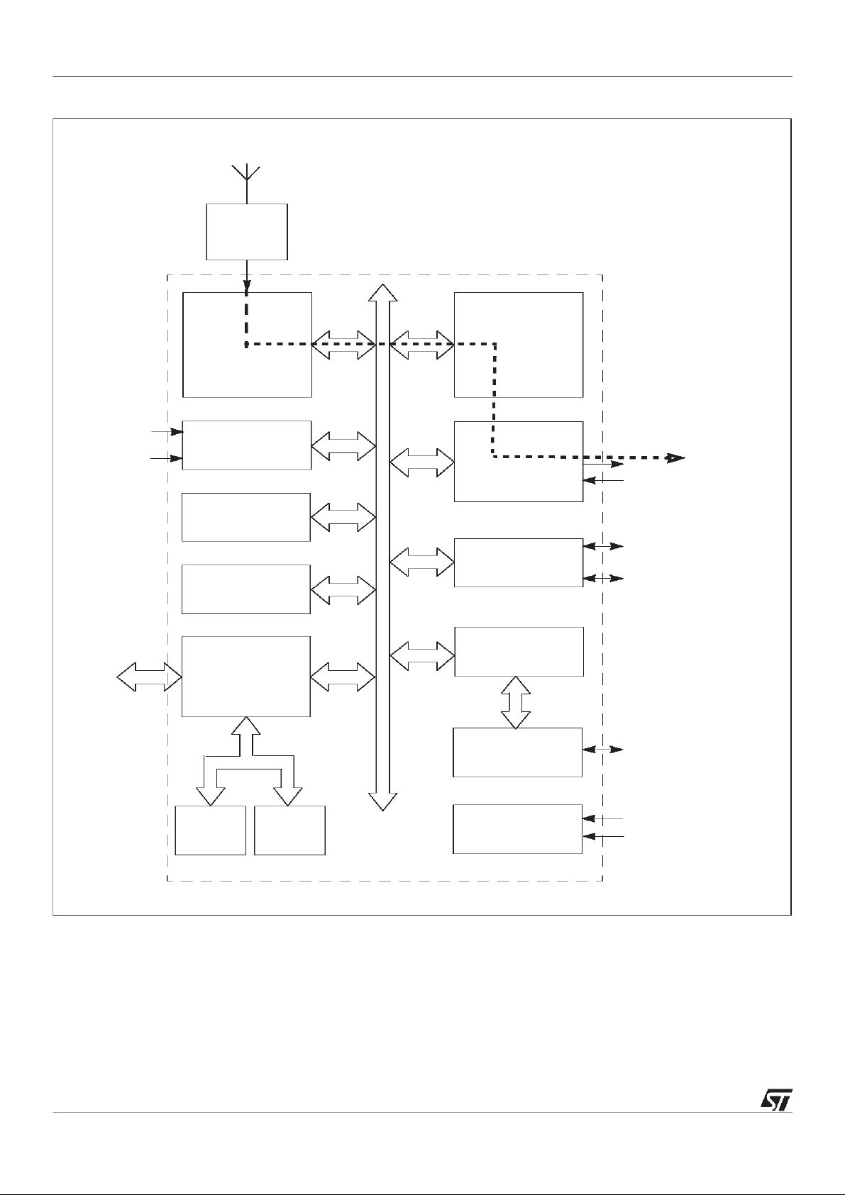
2 ST20-GP6 architecture overview
The ST20-GP6 consists of an ST20 CPU plus application specific DSP hardware for handling GPS
signals, plus a dual channel UART, ROM and RAM memory, parallel IO, real time clock and
watchdog functions.
Figure 2.1 shows the subsystem modules that comprise the ST20-GP6. These modules are
outlined below and more detailed information is given in the followingchapters.
DSP
The ST20-GP6 includes DSP hardware for processing signals from the GPS satellites. The DSP
module generates the pseudo-random noise (prn) signals, and de-spreads the incoming signal.
It consists of a down conversion stage that takes the 4 MHz input signal down to nominally zero
frequency both in-phase and quadrature (I & Q). This is followed by 12 parallel hardware channels
for satellite tracking, whose output is passed to the CPU for further software processing at a
programmableinterval, nominally every millisecond.
CPU
The Central Processing Unit (CPU) on the ST20-GP6 is the ST20 32-bit processor core. It contains
instruction processing logic, instruction and data pointers, and an operand register. It directly
accesses the high speed on-chip memory, which can store data or programs.The processor can
access up to 4 Mbytes of memory via the programmablememory interface.
7/123
Page 8
ST20-GP6
GPS
radio
ST20-GP6
Interrupts
12 channel GPS
hardware DSP
Interrupt
controller
Low
power
controller
Real time
clock
Programmable
memory
interface
ST20
CPU
Serial
communications
2 UART
Parallel
input/output
Diagnostic
control unit
Test access
port
User position
output in
ASCII
.
.
16
.
128K
ROM
64K
SRAM
System
services
Reset
Clock
Figure 2.1 ST20-GP6 architectural block diagram
Memory subsystem
The ST20-GP6 on-chip memory system provides 60 Mbytes/s internal data bandwidth, supporting
pipelined 2-cycle internal memory access at 30 ns cycle times. The ST20-GP6 memory system
consists of SRAM, ROMand a programmableexternal memory interface (EMI).
8/123
Page 9

ST20-GP6
The ST20-GP6 can use 8 or 16-bit external RAM, 8 or 16-bit external ROM, and has a 20-bit
address bus.
The ST20-GP6 product has 64 Kbytes of on-chip SRAM. This is in 4 banks of 16 Kbytes. One of
these banks is powered from the back-up battery supply.The ST20-GP6 has 128 Kbytes of ROM
for application code.
The ST20-GP6 memory interface controls the movement of data between the ST20-GP6 and offchip memory.It is designed to support memory subsystems without any external support logic and
is programmableto support a wide range of memory types. Memory is divided into 4 banks which
can each have different memory characteristics and each bank can access up to 1 Mbyte of
external memory.
The normal memory provision in a simple GPS receiver is a single 64K x 16-bit ROM or Flash
ROM (70, 90 or 100 ns access time). The internal 64 Kbyte RAM is sufficient for application use,
howeverfor development purposes external RAM may be added. The ST20-GP6 can supportup to
1 Mbyte of SRAM plus 1 Mbyte of ROM, enabling additional functions to be added if required.
Low power controller, real time clock and watchdog timer
The ST20-GP6 has power-down capabilities configurable in software. When powered down, a
timer can be used as an alarm, re-activating the CPU after a programmed delay.This is suitable for
ultra low power or solar powered applications such as container tracking, railway truck tracking, or
marine navigation buoysthat must checkthey are on station at intervals.
There is also a watchdog timer (WDT), resetting the system if it times out. The watchdog timer
function is enabled by an external pin (WdEnable). The WDT has a counter, clocked to give a
nominal 2 second delay.A status flag (notWdReset) is set by a watchdog reset. This can be used
to indicate to application code that the system wasreset by the watchdog timer.
The real time clock (RTC) provides a set of continuously running counters to provide a clockcalendar function. The counter values can be written to set the current time/data. The RTC is
clockedbya 32,768 Hz crystal oscillator and has a separate powersupply so that it cancontinue to
run when the rest of the chip is powereddown.
The RTC contains two counters: a 30-bit ‘milliseconds’ counter and a 16-bit ‘weeks’ counter. This
allows large time values to be represented to high accuracy. Note that the milliseconds counter is
actually clockedat 1.024 KHz and this must be handled by software.
The ST20-GP6 is designed for 0.35 micron, 3.3 V CMOS technology and runs at speeds of up to
50 MHz. 3.3 V operation provides reduced power consumption internally and allows the use of low
power peripherals. In addition, a power-down mode is available on the ST20-GP6.
The different power levels of the ST20-GP6 are listed below.
• Operating power — power consumed during functional operation.
• Stand-bypower — power consumed during little or no activity. The CPU is idle but ready to
immediately respond to an interrupt/reschedule.
• Power-down — clocks are stopped and power consumption is significantly reduced. Functional operation is stalled. Normal functional operation can be resumed from previous state
as soon as the clocks are stable. No information is lost during power down as all internal
logic is static.
9/123
Page 10

ST20-GP6
• Power to most of the chip removed— only the real time clock supply (RTCVDD) power on.
In power-downmode the processor and all peripherals are stopped, including the external memory
controller and optionally the PLL. Effectively the internal clock is stopped and functional operation
is stalled. On restart the clock is restarted and the chip resumes normal functional operation.
Serial communications
The ST20-GP6 has two UARTs (Asynchronous Serial Controllers (ASCs)) for serial
communication. The UARTs provide an asynchronous serial interface and can be programmed to
support a range of baud rates and data formats,for example,data size, stop bits and parity.
Interrupt subsystem
The ST20-GP6 interrupt subsystem supports eight prioritized interrupts. Four interrupts are
connected to on-chip peripherals (2 for the UARTs, 2 for the programmable IO), two are available
as external interrupt pins and two are spare.
Each interrupt level has a higher priority than the previous and each level supports only one
software handler process.
Note that interrupt handlers must not prevent the GPS DSP data traffic from being handled. During
continuous operation this has 1 ms latency and is not a problem, but during initial acquisition it has
a32µs rate and thus all interrupts must be disabledexcept if used to stop GPS operation.
Parallel IO module
Sixteen bits of parallel IO are provided. Each bit is programmableas an output or an input. Edge
detection logic is provided which can generate an interrupt on any change of an input bit.
JTAGTest Access Port
The Test Access Port (TAP) supports the IEEE 1149.1 JTAG test standard.
Diagnostic controller
The diagnostic controller is a programmablemodule which connects directly into the CPU.It can be
accessed by the TAP. This allows debugging systems to be used which do not affect CPU
performance or intrude into application code. Debugging support includes:
• hardware breakpoint and watchpoint
• real time trace
• external LSA triggering support
It is also used to provide system services, including booting the CPU.
System services module
The ST20-GP6 system services module includes:
• reset and initialization port.
• phase locked loop (PLL) — accepts 16.368 MHz input and generates all the internal high
frequency clocks needed for the CPU.
10/123
Page 11
ST20-GP6
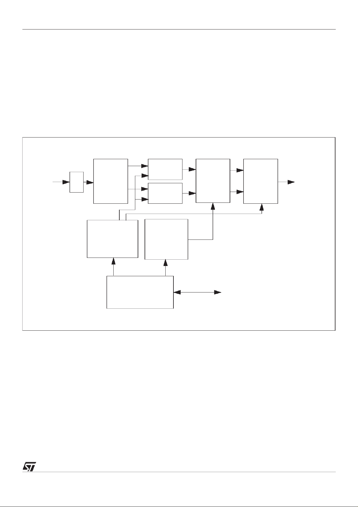
3 Digital signal processing module
The ST20-GP6 chip includes 12 channel GPS correlation DSP hardware. It is designed to handle
twelve satellites, two of which can be initialized to support the RTCA-SC159specification.
The digital signal processing (DSP) module extracts GPS data from the incoming IF (Intermediate
Frequency) data. There are a number of stages of processing involved; these are summarized
below and in Figure 3.1. After the 12 pairs of hardware correlators, the data for all channels are
time division multiplexed onto the appropriate internal buses (i.e. values for each channel are
passed in sequence, for example: I1,Q1,I2,Q2... I12,Q12,I1,Q1).
4 MHz IF
input
data
sampler
frequency
converter A
Pseudo random
noise sequence
generator
(x 12)
ST20 CPU accessible
registers
I correlator
(x 12)
Q correlator
(x 12)
Numerically
controlled
oscillator
frequency
converter B
DMA
interface
accumulator
Figure 3.1 DSP module blockdiagram
The main stages of processing are as follows:
Data sampling
This stage removes any meta-stability caused by the asynchronous input data coming from an
analogue source (the radio receiver). The data at this point consists of a carrier of nominally
4.092 MHz with a bandwidth of approximately±1 MHz.
This stage is common to all 12 channels.
11/123
Page 12

ST20-GP6
Frequency conversion (A)
The first frequency converter mixes the sampled IF data with the (nominal) 4.092 MHz signal. This
is done twice with a quarter cycle offset to produce I and Q (In-phase and Quadrature) versions of
the data at nominal zero centre frequency (this can actually be up to ±132 KHz due to errors such
as doppler shift, crystal accuracy,etc.). The sum frequency (~8 MHz) is removedby low-pass filtering in the correlator.
This stage is common to all 12 channels.
Correlation against pseudo-random sequence
The GPS data is transmitted as a spread-spectrum signal (with a bandwidth of about 2 MHz). In
order to recover the data it is necessary to correlate against the same Pseudo-Random Noise
(PRN) signal that was used to transmit the data. The output of the correlator accumulator is sampled at 264 KHz. The PRN sequences come from the PRN generator.
There is a correlator for the I and Q signals for each of the 12 channels. The output signal is now
narrowband.
Frequency conversion (B)
The second stage of frequency conversion mixes the data with the local oscillator signal generated
bythe Numerically Controlled Oscillator (NCO). This signal is locked, under software control, to the
Space Vehicle (SV) frequency and phase to remove the errors and take the frequency and bandwidth of the data down to 0 and ±50 Hz respectively.Filtering to 500 Hz is achievedin hardware,to
50 Hz in software.
This stage is shared by time division multiplexing between all 12 channels. This is loss-free as the
stage supports 12 channels x 264 KHz, approximately 3 MHz, well within its 16 MHz clock rate.
Result integration
The final stage sums the I and Q values for each channel over a user defined period. In normal
operation, the sampling period is slightly less than the 1ms length of the PRN sequence. This
ensures that no data is lost, although it may mean that some data samples are seen twice — this is
handled (mainly) in software.
The sampling period can also be programmed to be much shorter (i.e. a higher cut-off frequency
for the filter) when the system is trying to find new satellites (‘acquisition mode’).
There are two further stages of buffering for the accumulated 16-bit I and Q values for each channel. These allow for the slightly differenttime domains involved1.
The results after hardware processing of the signal, using the parameters set in the DSP registers,
refer to Section 3.1, are delivered to the CPU via a DMA engine in packet format. The CPU should
perform an
in
(input) instruction on the appropriate channel (see address map, Figure 8.1 on
page 53) in order to read a packet.
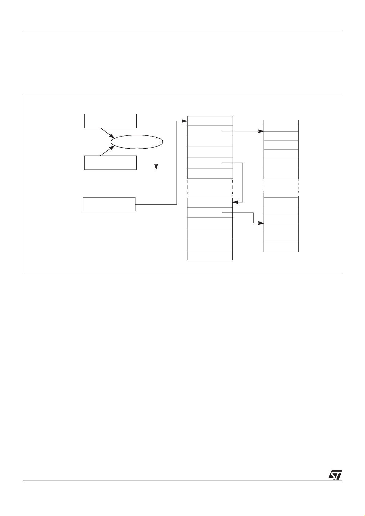
The format of the 62-byte packets is given in Figure 3.2. These represent a two byte header, fol-
lowedby the 16-bit I-valuesfor 12 channels, then the 16-bit Q-values for 12 channels, then the 8-bit
timestamp values for the 12 channels. The I and Q values are sent least significantbyte first. The 2
1. Data sampled in SV time, data transmitted to the CPU at fixedintervals.
12/123
Page 13

ST20-GP6
byte header contains: a ‘sync’ byte with the value #1B, and a ‘sample rate’ byte which contains the
two SampleRate bits from the DSPControl register,see Table3.1.
Packetsare delivered at the rate selected by the DSPControl register, evenif new data is not available. In this case, the data value for the field is set to #8000. This guarantees that synchronism is
maintained between the satellite one-millisecond epochs and the receiver, despite time-of-reception variations due to the varying path length from the satellite.
62 byte packet every 840/970/31/62 µs
16-bit
header
sync
12 x 16-bit
I values
sample
rate
12 x 16-bit
Q values
Absent 16-bit values padded with #8000
Trackingmode
T[7:6] = 10
T[5:0] = time[5:0]
Figure 3.2 DSP packet format
12 x 8-bit
time values
Acquisition mode
First packet (in SV ms)
T[7:6] = 10
T[5:0] = time[5:0]
Remaining packets
T[7:6] = 00
T[5:0] = sequence number
(sequence numbers are 2 to
16 or 32)
3.1 DSP module registers
The GPS hardware channels of the ST20-GP6 are controlled bythree sets of registers:
1 DSPControl register
2 PRNcode0-11 and PRNphase0-11 registers
3 NCOfrequency0-11 and NCOphase0-11 registers
The base addresses for the DSP registers are given in the Memory Map chapter.
DSPControl register
The DSPControl register determineswhether the PRN generators are on (normal use) or disabled
(for built-in-self-test of a system), whether the system is in tracking mode (840/970 µs output rate)
or initial acquisition mode (31/62 µs), and selects which of the two rates for each mode. It also
13/123
Page 14

ST20-GP6
determines whether the accumulated carrier phase in the NCO are reset to zero automatically or
continue from their existing value. The bit allocations are givenin Table3.1.
DSPControl DSP base address + #140 Write only
Bit Bit field Function
1:0 SampleRate These bits control the sampling rate (the rate at which data is sent to the DMA
controller). The encoding of these bits is as follows:
SampleRate[1:0] Transfer period
00 840 µs 256 Tracking
01 970 µs 256
10 31 µs 8 Acquisition
11 62 µs16
2NCOResetEnable When set to 1, the accumulated NCO phase for a channel is reset when the cor-
responding PRN code register is written.
3 PRNDisable When set to 1, all PRN generators are disabled.
No. of samples
accumulated
Mode
Table3.1 DSPControl register format
PRNcode0-11 registers
The PRNcode0-11 registers choose the code for the particular satellite, and writing these causes a
reset to the accumulated carrier phase in the NCO for the corresponding channel, if enabledby the
DSPControl register.
PRNcode0-11 DSP base address + #00 to #2C Write only
Bit Bit field Function
6:0 PRNcode Satellite code as a 7-bit value.
Table3.2 PRNcode0-11 register format
The bit-fields for selecting particular GPS satellites are given in Table3.3.
14/123
Page 15

ST20-GP6
Satellite ID
1 #62 6 2
2 #73 7 3
3 #04 8 4
4 #15 9 5
5 #11 9 1
6 #22 10 2
7 #01 8 1
8 #12 9 2
9 #23 10 3
10 #32 3 2
11 #43 4 3
12 #65 6 5
13 #76 7 6
14 #07 8 7
15 #18 9 8
16 #29 10 9
17 #41 4 1
18 #52 5 2
19 #63 6 3
20 #74 7 4
21 #05 8 5
22 #16 9 6
23 #31 3 1
24 #64 6 4
25 #75 7 5
26 #06 8 6
27 #17 9 7
28 #28 10 8
29 #61 6 1
30 #72 7 2
31 #03 8 3
32 #14 9 4
- #25 10 5
- #24 10 4
- #71 7 1
- #02 8 2
- #24 10 4
b
WAAS
PRNcode0-11
register value
#20 10 0
Taps selected from G2 shift register
by bits 6 to 4 by bits 3 to 0
a
Table 3.3 PRNcode0-11 register value
a. Refer to the US DoD document ICD-GPS-200.
b. It is the responsibility of the software to ensure that when this value is selected, a suitable
value has been written into the PRNinitialVal0-1 register. If this channel is later used fora
standard GPS satellite, the PRNinitialVal0-1 must be set to all ones (#3FF).
For channels 0 and 1, RTCA-SC159 satellite codes can also be selected. This is achieved by setting the PRNcode0-11 register appropriately and also writing the initial value for the satellite to the
15/123
Page 16

ST20-GP6
PRNinitialVal0-1 register, see Table3.8. If uninitialized by the software, the PRNinitialVal register
defaults to 11 1111 1111 (#3FF) as required for GPS satellites.
The PRNcode0-11 and PRNinitialVal0-1 registers are normally written only when the satellite is
first chosen.
PRNphase0-11 registers
The PRN0-11phase registers determine the relativedelay between the receiver master clock, and
the start of the one millisecond repetitive code sequence. The code sequence starts when the
receiver clock counter (invisible to the software except through message timestamps) reaches the
value written to the PRNphase0-11 register. The PRNphase0-11 register must only be written
once per satellite milliseconds-epoch, which varies from the receiver epoch dynamically due to satellite motion. Synchronism with the software is achieved by reading the register, when a write
enable flag is returned. If not enabled, the write operation is abandoned by the software.
The 19-bit valuecomprises three fields.The 3 least significant bits represent the fractional-delay in
eighths of a code-chip. The middle 10 bits represent the integer delay in code-chips, 0-1022, with
the value 1023 illegal. The upper 6 most significant bits represent the delay in integer milliseconds.
PRNphase0-11 DSP base address + #40 to #6C Write only
Bit Bit field Function
2:0 FractionalDelay Fractional delay in eighths of a code-chip.
12:3 IntegerDelay Integer delay in code-chips. Value 0-1022. Note, the value 1023 is illegal.
18:13 Delay Delay in integer milliseconds.
Table 3.4 PRNphase0-11 register format
Note also that the eighth-chip resolution of the code generator is not sufficient for positioning. At
125 ns it represents approximately40 m of range,over 100 m of position. The software must maintain the range measurements around the 1 ns resolution level in a 32-bit field, and send an appropriate 19-bit sub-field to the register. Note, care must be taken when calculating this field from a
computed delay,or vice versa,to allow forthe missing value1023. The overallregister bit-field cannot be used mathematically as a single binary number.
PRNphase0-11WrEn registers
The PRNphase0-11WrEn flags are active low flags that record when the PRNphase0-11 register
can be updated. The PRNphaseWrEn flag for a channel is set high when the corresponding PRN-
phase register is written. The flag is reset again when the value written is loaded into the PRN gen-
16/123
Page 17

ST20-GP6
erator. Note, the PRNphase0-11 register should only be updated when the PRNphase0-11WrEn
register has been cleared by the hardware.
PRNphase0-11WrEn DSP base address + #40 to #6C Read only
Bit Bit field Function
0 PRNphaseWrEn
Set when the corresponding PRNphase0-11 register is set.
Table3.5 PRNphase0-11WrEn register format
NCOfrequency0-11 registers
The NCOfrequency0-11 registers hold a signed 18-bit value that is added repetitively, ignoring
overflows, to the accumulated NCO phase from which the NCO sine and cosine waveforms are
generated. The addition is performed at a 264 KHz rate (16.368MHz/62). The accumulated NCO
phase is not accessible to the software, but can be cleared when initialising the channel if enabled
by the DSPControl register.
Each unit value in the NCOfrequency0-11 register represents 264KHz/(218), i.e.
1.007080078125 Hz.
If the extreme values are written, #1FFFF and #20000, the sine wave generated will be at approxi-
mately +132 KHz, and precisely -132 KHz respectively.
NCOfrequency0-11 DSP base address + #80 to #AC Write only
Bit Bit field Function
17:0 NCOfrequency NCO frequency as a signed 18-bit value.
Table 3.6 NCOfrequency0-11 register format
NCOphase0-11 registers
The NCOphase0-11 registers contents are added to the accumulated phase to correct the carrier
for the final 1 Hz that cannot be resolved by the NCO frequency.This addition is not cumulative,
and the value must be updated regularly by the software as a result of carrier phase errors measured on the satellite signal. The register holds a signed 7-bit field representing +/-180 degrees
total in steps of 2.8125 degrees(360/128).
NCOphase0-11 DSP base address + #C4 to #EC Write only
Bit Bit field Function
6:0 NCOphase NCO phase as a signed 7-bit value representing +/-180 degrees total in steps of
2.8125 degrees (360/128).
Table 3.7 NCOphase0-11 register format
17/123
Page 18

ST20-GP6
PRNinitialVal0-1 registers
The initial value for the two RTCA-SC159 capable satellites channels should be written to the
PRNinitialVal0-1 registers. The value can be foundin the
RTCA-SC159 Specification
.
Note: The value written to the register is the Initial Value defined by RTCA-SC159 for the PRN
required. The conversion from ‘big-endian’ as used in the specification to ‘little-endian’ as conventionally used in ST20 architectures has been implemented in the hardware.
If uninitialized by the software, this register defaults to 11 1111 1111 (#3FF) as required for GPS
satellites.
PRNinitialVal0-1 DSP base address + #100, #104 Write only
Bit Bit field Function
9:0 InitialValue Initial value of the RTCA-SC159 satellite channel.
Table 3.8 PRNinitialVal0-1 register format
18/123
Page 19

ST20-GP6
4 Central processing unit
The Central Processing Unit (CPU) is the ST20 32-bit processor core. It contains instruction processing logic,instruction and data pointers, and an operand register. It can directly access the high
speed on-chip memory, which can store data or programs. Where larger amounts of memory are
required, the processor can access memory via the External Memory Interface (EMI).
The processor provides high performance:
• Fast integer multiply - 4 cycle multiply
• Fast bit shift - single cycle barrel shifter
• Byte and part-wordhandling
• Scheduling and interrupt support
• 64-bit integer arithmetic support.
The scheduler provides a single level of pre-emption. In addition, multi-level pre-emption is provided by the interrupt subsystem, see Chapter 5 for details. Additionally, there is a per-priority trap
handler to improvethe support for arithmetic errors and illegal instructions,refer to section 4.6.
4.1 Registers
The CPU contains six registers which are used in the execution of a sequential integer process.
The six registers are:
• The workspace pointer (Wptr) which points to an area of store where local data is kept.
• The instruction pointer (Iptr) which points to the next instruction to be executed.
• The status register (Status).
• The Areg, Breg and Creg registers which form an evaluationstack.
The Areg, Breg and Creg registers are the sources and destinations for most arithmetic and logical operations.Loading a value into the stack pushes Breg into Creg, and Areg into Breg, before
loading Areg. Storing a value from Areg, pops Breg into Areg and Creg into Breg. Creg is left
undefined.
Local data ProgramRegisters
Areg
Breg
Creg
Wptr
Iptr
Figure 4.1 Registers used in sequential integer processes
19/123
Page 20

ST20-GP6
Expressions are evaluated on the evaluationstack, and instructions refer to the stack implicitly. For
example,the
the stack. The use of a stack removes the need for instructions to explicitly specify the location of
their operands. No hardware mechanism is provided to detect that more than three values have
been loaded onto the stack; it is easy for the compiler to ensure that this neverhappens.
Note that a location in memory can be accessed relative to the workspace pointer, enabling the
workspace to be of any size.
The use of shadow registers provides fast, simple and clean contextswitching.
add
instruction adds the top twovaluesin the stack and places the result on the top of
4.2 Processes and concurrency
The following section describes ‘default’ behavior of the CPU and it should be noted that the user
can alter this behavior,for example,by disabling timeslicing, installing a user scheduler,etc.
A process starts, performs a number of actions, and then either stops without completing or terminates complete. Typically, a process is a sequence of instructions. The CPU can run several processes in parallel (concurrently). Processes may be assigned either high or low priority, and there
maybe any number of each.
The processor has a microcoded scheduler which enables any number of concurrent processes to
be executed together, sharing the processor time. This removes the need for a software kernel,
although kernels can still be written if desired.
At any time, a process may be
active
inactive
The scheduler operates in such a way that inactive processes do not consume any processor time.
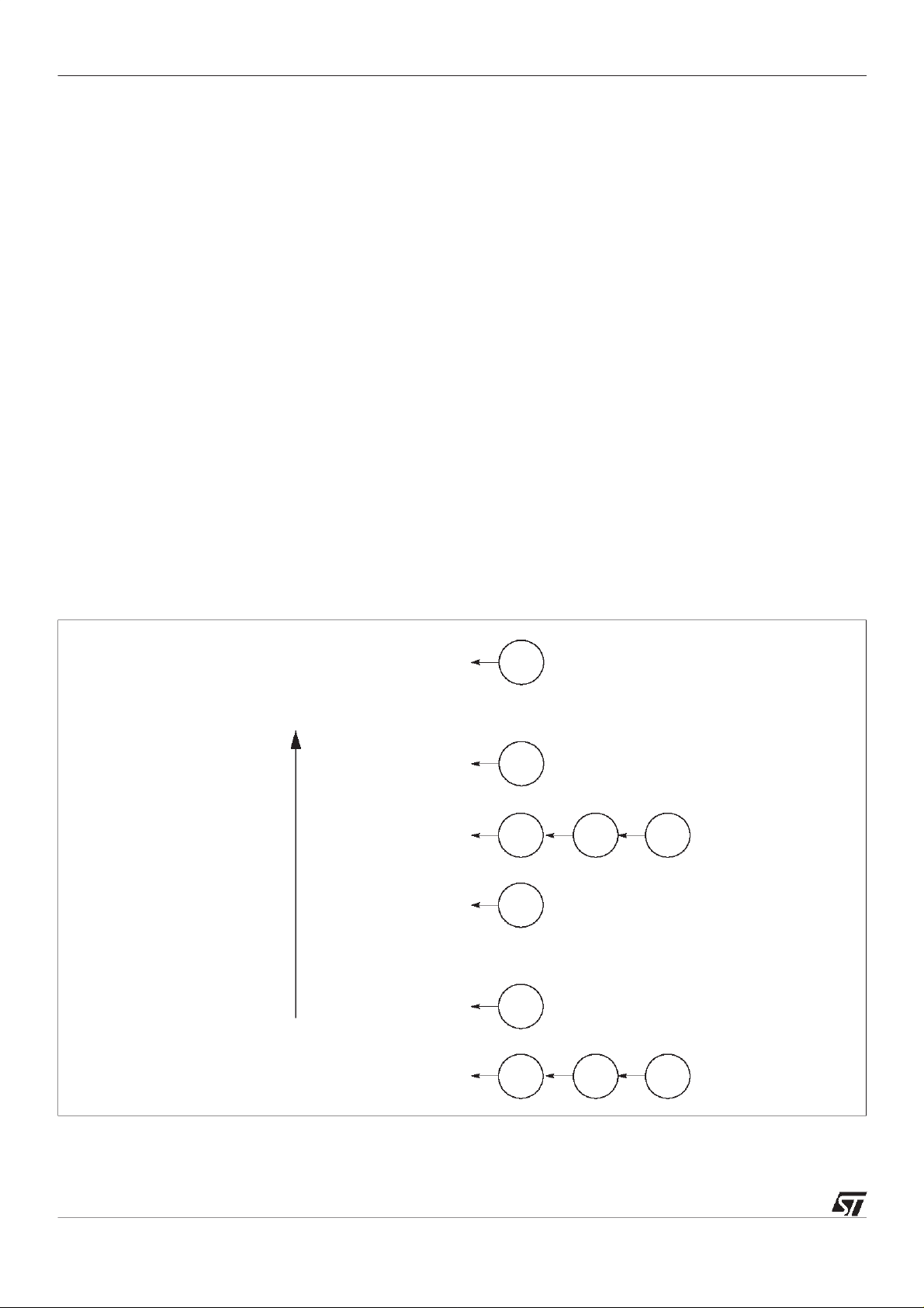
Each active high priority process executesuntil it becomes inactive.The scheduler allocates a portion of the processor’stime to each active low priority process in turn (see section 4.3). Active processes waiting to be executed are held in two linked lists of process work spaces, one of high
priority processes and one of low priority processes. Each list is implemented using two registers,
one of which points to the first process in the list, the other to the last. In the linked process list
shown in Figure 4.2, processSis executing andP,QandRare active, awaiting execution. Only the
low priority process queue registers are shown; the high priority process ones behavein a similar
manner.
- being executed,
- interrupted by a higher priority process,
- on a list waiting to be executed.
- waiting to input,
- waiting to output,
- waiting until a specifiedtime.
20/123
Page 21

ST20-GP6
Registers
FptrReg1
BptrReg1
Areg
Breg
Creg
Wptr
Iptr
Local data
P
Q
R
S
Iptr.s
Link.s
Iptr.s
Link.s
Iptr.s
Program
Figure 4.2 Linked process list
Function High priority Low priority
Pointer to front of active process list
Pointer to back of active process list
FptrReg0 FptrReg1
BptrReg0 BptrReg1
Table4.1 Priority queue control registers
Each process runs until it has completed its action or is descheduled. In order for several processes to operate in parallel, a low priority process is only permitted to execute for a maximum of
two timeslice periods. After this, the machine deschedules the current process at the next timeslicing point, adds it to the end of the low priority scheduling list and instead executes the next active
process. The timeslice period is 1ms.
There are only certain instructions at which a process may be descheduled. These are known as
descheduling points. A process may only be timesliced at certain descheduling points. These are
known as timeslicing points and are defined in such a way that the operand stack is always empty.
This removes the need for saving the operand stack when timeslicing. As a result, an expression
evaluation can be guaranteed to executewithout the process being timesliced part waythrough.
Whenevera process is unableto proceed, its instruction pointer is savedin the process workspace
and the next process takenfrom the list.
The processor core provides a number of special instructions to supportthe process model, including
startp
struct,
(start process) and
startp
is used to create the necessary additional concurrent processes. A
endp
(end process). When a main process executes a parallel con-
startp
instruction
creates a new process by adding a new workspace to the end of the scheduling list, enabling the
new concurrent process to be executed together with the ones already being executed. When a
process is made active it is always added to the end of the list, and thus cannot pre-empt processes already on the same list.
The correct termination of a parallel construct is assured by use of the
endp
instruction. This uses
a data structure that includes a counter of the parallel construct components which have still to ter-
21/123
Page 22

ST20-GP6
minate. The counter is initialized to the number of components before the processes are started.
Each component ends with an
the last component, the counter is non zero and the component is descheduled. For the last component, the counter is zero and the main process continues.
endp
instruction which decrements and tests the counter.Forall but
4.3 Priority
The following section describes ‘default’ behavior of the CPU and it should be noted that the user
can alter this behavior,for example,by disabling timeslicing and priority interrupts.
The processor can executeprocesses at one of two priority levels, one level for urgent (high priority) processes, one for less urgent (low priority) processes. A high priority process will alwaysexecute in preferenceto a low priority process if both are able to do so.
High priority processes are expected to execute for a short time. If one or more high priority processes are active, then the first on the queue is selected and executesuntil it has to wait for a communication, a timer input, or until it completes processing.
If no process at high priority is active, but one or more processes at low priority are active, then one
is selected. Low priority processes are periodically timesliced to provide an evendistribution of processor time between tasks which use a lot of computation.
If there arenlowpriority processes, then the maximum latency from the time at which a low priority
process becomes active to the time when it starts processing is the order of 2ntimeslice periods. It
is then able to execute for between one and two timeslice periods, less any time taken by high priority processes. This assumes that no process monopolizes the time of the CPU; i.e. it has frequent timeslicing points.
The specific condition for a high priority process to start executionis that the CPU is idle or running
at low priority and the high priority queue is non-empty.
If a high priority process becomes able to run while a low priority process is executing, the low priority process is temporarily stopped and the high priority process is executed. The state of the low
priority process is savedinto ‘shadow’ registers and the high priority process is executed.When no
further high priority processes are able to run, the state of the interrupted lowpriority process is reloaded from the shadow registers and the interrupted low priority process continues executing.
Instructions are provided on the processor core to allow a high priority process to store the shadow
registers to memory and to load them from memory. Instructions are also provided to allow a process to exchange an alternative process queue foreither priority process queue (see Table7.21 on
page 49). These instructions allow extensions to be made to the scheduler for custom run-time kernels.
A low priority process may be interrupted after it has completed execution of any instruction. In
addition, to minimize the time taken for an interrupting high priority process to start executing, the
potentially time consuming instructions are interruptible. Also some instructions may be aborted,
and are restarted when the process next becomes active (refer to the Instruction Set chapter).
22/123
Page 23

ST20-GP6
4.4 Process communications
Communication between processes takes place over channels, and is implemented in hardware.
Communication is point-to-point, synchronized and unbuffered. As a result, a channel needs no
process queue, no message queue and no message buffer.
A channel between two processes executing on the same CPU is implemented by a single word in
memory; a channel between processes executingon differentprocessors is implemented by pointto-point links. The processor provides a number of operations to support message passing, the
most important beingin(input message) and
out
(output message).
Theinand
out
instructions use the address of the channel to determine whether the channel is
internal or external. This means that the same instruction sequence can be used for both hard and
soft channels, allowing a process to be written and compiled without knowledge of where its channels are implemented.
Communication takes place when both the inputting and outputting processes are ready. Consequently, the process which first becomes ready must wait until the second one is also ready. The
inputting and outputting processes only become activewhen the communication has completed.
A process performs an input or output by loading the evaluationstack with, a pointer to a message,
the address of a channel, and a count of the number of bytes to be transferred,and then executing
aninor
out
instruction.
4.5 Timers
There are two 32-bit hardware timer clocks which ‘tick’ periodically. These are independent of any
on-chip peripheral real time clock. The timers provide accurate process timing, allowing processes
to deschedule themselves until a specifictime.
One timer is accessible only to high priority processes and is incremented approximately every
microsecond, cycling completely in approximately 4295 seconds. The other is accessible only to
low priority processes and is incremented approximately every 64 microseconds, giving 15625
ticks per second. It has a full period of approximately 76 hours. Timer frequencies are approximate.
Register Function
ClockReg0 Current value of high priority (level 0) process clock.
ClockReg1 Current value of low priority (level1) process clock.
TnextReg0 Indicates time of earliest eventon high priority (level0) timer queue.
TnextReg1 Indicates time of earliest eventon low priority (level 1) timer queue.
TptrReg0 High priority timer queue.
TptrReg1 Low priority timer queue.
Table4.2 Timer registers
The current value of the processor clockcan be read by executinga
A process can arrange to perform a
after a specified time has been reached. The
tin
(timer input), in which case it will become ready to execute
tin
instruction requires a time to be specified. If this
ldtimer
(load timer) instruction.
time is in the ‘past’ then the instruction has no effect. If the time is in the ‘future’ then the process is
descheduled. When the specified time is reached the process becomes active. In addition, the
23/123
Page 24
ST20-GP6
ldclock
clockenb
(load clock),
(clock enable),
stclock
(store clock) instructions allow total control over the clock value and the
clockdis
(clock disable) instructions allow each clock to be individually
stopped and re-started.
Figure 4.3 shows two processes waiting on the timer queue, one waiting for time 21, the other for
time 31.
Work spaces
ClockReg0
TnextReg0
TptrReg0
5
Comparator
21
Alarm
21
Program
Empty
31
Figure 4.3 Timer registers
4.6 Trapsand exceptions
A software error, such as arithmetic overflow or array bounds violation, can cause an error flag to
be set in the CPU.The flag is directly connected to the ErrorOut pin. Both the flagand the pin can
be ignored, or the CPU stopped. Stopping the CPU on an error means that the error cannot cause
further corruption. As well as containing the error in this wayit is possible to determine the state of
the CPU and its memory at the time the error occurred. This is particularly useful for postmortem
debugging where the debugger can be used to examine the state and history of the processor
leading up to and causing the error condition.
In addition, if a trap handler process is installed, a variety of traps/exceptions can be trapped and
handled by software. A user supplied trap handler routine can be provided for each high/low process priority level. The handler is started when a trap occurs and is given the reason for the trap.
The trap handler is not re-entrant and must not cause a trap itself within the same group. All traps
can be individually masked.
4.6.1 Trap groups
The trap mechanism is arranged on a per priority basis. For each priority there is a handler for each
group of traps, as shown in Figure 4.4.
24/123
Page 25

Low priority traps High priority traps
ST20-GP6
Breakpoint
trap handler
CPU Error
trap handler
System operations
trap handler
Scheduler
trap handler
Figure 4.4 Traparrangement
There are four groups of traps, as detailed below.
• Breakpoint
This group consists of the
Breakpoint
trap. The breakpoint instruction (j0) calls the break-
point routine via the trap mechanism.
• Errors
The traps in this group are
IntegerError
and
flow, such as arithmetic results which do not fit in the result word.
errors caused when data is erroneous, for example when a range checking instruction finds
that data is out of range.
• System operations
This group consists of the
LoadTrap,StoreTrap
trap is signalled when an attempt is made to execute an illegal instruction. The
and
StoreTrap
traps allow a kernel to intercept attempts by a monitored process to change
or examine trap handlers or trapped process information. It enables a user program to signal to a kernel that it wishes to install a new trap handler.
CPU Error
trap handler
Breakpoint
trap handler
Overflow.Overflow
and
IllegalOpcode
Scheduler
trap handler
System operations
trap handler
represents arithmetic over-
IntegerError
traps. The
represents
IllegalOpcode
LoadTrap
• Scheduler
The scheduler trap group consists of the
TimeSlice, Run, Signal, ProcessInterrupt
ExternalChannel, InternalChannel, Timer,
and
QueueEmpty
traps. The
ProcessInterrupt
trap signals that the machine has performed a priority interrupt from low to high. The
QueueEmpty
trap indicates that there is no further executable work to perform. The other
traps in this group indicate that the hardware scheduler wants to schedule a process on a
process queue, with the different traps enabling the different sources of this to be monitored.
The scheduler traps enable a software scheduler kernel to use the hardware scheduler to
implement a multi-priority software scheduler.
Note that scheduler traps are different from other traps as they are caused by the microscheduler rather than by an executing process.
Trap groups encoding is shown in Table 4.3 below.These codes are used to identify trap groups to
various instructions.
25/123
Page 26

ST20-GP6
Trapgroup Code
Breakpoint 0
CPU errors
System operations
Scheduler 3
1
2
Table 4.3 Trap group codes
In addition to the trap groups mentioned above,the CauseError flag in the Status register is used
to signal when a trap condition has been activated by the
causeerror
instruction. It can be used to
indicate when trap conditions have occurred due to the user setting them, rather than by the system.
4.6.2 Events that can cause traps
Table4.4 summarizes the events that can cause traps and gives the encoding of bits in the trap
Status and Enable words.
Trapcause
Breakpoint
IntegerError
Status/Enable
codes
00
1 1 Integer error other than integer overflow - e.g. explicitly checked or
Trap
group
Comments
When a process executesthe breakpoint instruction (j0) then it traps
to its trap handler.
explicitly set error.
Overflow
IllegalOpcode
LoadTrap
StoreTrap
InternalChannel
ExternalChannel
Timer
Timeslice
Run
Signal
ProcessInterrupt
QueueEmpty
CauseError
21
3 2 Attempt to executean illegal instruction. This is signalled when
42
52
63
7 3 Scheduler trap from external channel.
83
93
10 3 Scheduler trap from
11 3
12 3
13 3 Caused by no process active at a priority level.
15 (Status only) Any,
encoded
0-3
Integer overflowor integer division by zero.
executedwith an invalid operand.
When the trap descriptor is read with the
the trappedprocess status is read with the
When the trap descriptor is written with the
when the trapped process status is written with the
instruction.
Scheduler trap from internal channel.
Scheduler trap from timer alarm.
Scheduler trap from timeslice.
runp
(run process) or
Scheduler trap from
Start executing a process at a new priority level.
Signals that the
signal
causeerror
.
instruction set the trap flag.
ldtraph
ldtrapped
sttraph
startp
opr
instruction or when
instruction.
instruction or
sttrapped
(start process).
is
26/123
Table 4.4 Trapcauses and Status/Enable codes
Page 27

ST20-GP6
4.6.3 Trap handlers
For each trap handler there is a trap handler structure and a trapped process structure. Both the
trap handler structure and the trapped process structure are in memory and can be accessed via
instructions, see section 4.6.4.
The trap handler structure specifies what should happen when a trap condition is present, see
Table4.5.
The trapped process structure saves some of the state of the process that was running when the
trap was taken, see Table4.6.
In addition, for each priority,there is an Enables register and a Status register. The Enables register contains flags to enable each cause of trap.The Status register contains flags to indicate which
trap conditions have been detected. The Enables and Status register bit encodings are given in
Table4.4.
Comments Location
Iptr Iptr of trap handler process. Base + 3
Wptr Wptr of trap handler process. A null Wptr indicates that a trap handler has not been installed. Base + 2
Status Contains the Status register that the trap handler starts with. Base + 1
Enables
A word which encodes the trap enable and global interrupt masks, which will be ANDed with
the existingmasks to allow the trap handler to disable various events while it runs.
Base + 0
Table4.5 Traphandler structure
Comments Location
Iptr Pointsto the instruction after the one that caused the trap condition. Base + 3
Wptr Wptr of the process that was running when the trap was taken. Base + 2
Status The relevant trap bit is set, see Table 4.3 for trap codes. Base + 1
Enables Interrupt enables. Base + 0
Table 4.6 Trapped process structure
A trap will be taken at an interruptible point if a trap is set and the corresponding trap enable bit is
set in the Enables register. If the trap is not enabled then nothing is done with the trap condition. If
the trap is enabled then the corresponding bit is set in the Status register to indicate the trap condition has occurred.
When a process takes a trap the processor saves the existing Iptr, Wptr, Status and Enables in
the trapped process structure. It then loads Iptr, Wptr and Status from the equivalent trap handler
structure and ANDs the value in Enables with the value in the structure. This allows the user to disable various events while in the handler, in particular a trap handler must disable all the traps of its
trap group to avoidthe possibility of a handler trappingto itself.
The trap handler then executes. The values in the trapped process structure can be examined
using the
ldtrapped
instruction (see section 4.6.4). When the trap handler has completed its opera-
27/123
Page 28

ST20-GP6
tion it returns to the trapped process via the
tret
(trap return) instruction. This reloads the values
savedin the trapped process structure and clears the trap flag in Status.
Note that when a trap handler is started, Areg, Breg and Creg are not saved. The trap handler
must save the Areg, Breg, Creg registers using
stl
(store local).
4.6.4 Trap instructions
Trap handlers and trapped processes can be set up and examined via the
ldtrapped
and
sttrapped
instructions. Table4.7 describes the instructions that may be used when
ldtraph,sttraph
dealing with traps.
Instruction Meaning Use
ldtraph
sttraph
ldtrapped
sttrapped
trapenb
trapdis
tret
load trap handler Load the trap handler from memory to the trap handler descriptor.
store trap handler Store an existingtrap handler descriptor to memory.
load trapped Load replacement trapped process status from memory.
store trapped Store trapped process status to memory.
trap enable Enable traps.
trap disable Disable traps.
trap return Used to return from a trap handler.
,
causeerror
cause error Program can simulate the occurrence of an error.
Table 4.7 Instructions which maybe used when dealing with traps
The first fourinstructions transfer data to/from the trap handler structures or trapped process structures from/to an area in memory. In these instructions Areg contains the trap group code (see
Table4.3) and Breg points to the 4 word area of memory used as the source or destination of the
transfer. In addition Creg contains the priority of the handler to be installed/examined in the case of
ldtraphorsttraph. ldtrapped
If the
LoadTrap
trap is enabled then
LoadTrap trap flag. If the
and
sttrapped
StoreTrap
apply only to the current priority.
ldtraph
and
ldtrapped
trap is enabled then
do not perform the transfer but set the
sttraph
and
sttrapped
do not perform the
transferbut set the StoreTrap trap flag.
The trap enable masks are encoded by an array of bits (see Table 4.4) which are set to indicate
which traps are enabled. This array of bits is stored in the lower half-word of the Enables register.
There is an Enables register for each priority.Trapsare enabledor disabled by loading a mask into
Areg with bits set to indicate which traps are to be affected and the priority to affect in Breg. Executing
for the priority in Breg. Executing
trapenb
ORs the mask supplied in Areg with the trap enables mask in the Enables register
trapdis
negates the mask supplied in Areg and ANDs it with the
trap enables mask in the Enables register for the priority in Breg. Both instructions return the previous value of the trap enables mask in Areg.
28/123
Page 29

ST20-GP6
4.6.5 Restrictions on trap handlers
There are various restrictions that must be placed on trap handlers to ensure that they work correctly.
1 Trap handlers must not deschedule or timeslice. Trap handlers alter the Enables masks,
therefore they must not allow other processes to executeuntil theyhave completed.
2 Trap handlers must have their Enable masks set to mask all traps in their trap group to
avoid the possibility of a trap handler trapping to itself.
3 Trap handlers must terminate via the
is that a scheduler kernel may use
restart
tret
(trap return) instruction.The only exception to this
to return to a previously shadowed process.
29/123
Page 30
ST20-GP6
5 Interrupt controller
The ST20-GP6 supports external interrupts, enabling an on-chip subsystem or external interrupt
pin to interrupt the currently running process in order to run an interrupt handling process
The ST20-GP6 interrupt subsystem supports eight prioritized interrupts. This allows nested preemptive interrupts for real-time system design. In addition, there is an interrupt level controller
(refer to Chapter 6) which multiplexes incoming interrupts onto the eight programmable interrupt
levels.This multiplexing is controllable by software. There are 6 sources of interrupts. Four of these
are internal (2 for the UARTs,2 for the programmableIO) and two are external.
All interrupts are a higher priority than the low priority process queue. Each interrupt can be programmed to be at a lower priority or a higher priority than the high priority process queue, this is
determined by the Priority bit in the HandlerWptr0-7 registers, see Table 5.1 on page 33.
Note: Interrupts (Interrupt0-7) which are specified as higher priority must be contiguous from the
highest numbered interrupt downwards,i.e. if 4 interrupts are programmed as higher priority and 4
as lower priority the higher priority interrupts must be Interrupt7:4 and the lower priority interrupts
Interrupt3:0.
Note that interrupt handlers must not prevent the GPS DSP data traffic from being handled. During
continuous operation this has 1 ms latency and is not a problem, but during initial acquisition it has
a32µs rate and thus care must be taken with interrupt priorities unless used to stop GPS opera-
tion.
Interrupt 7
when Priority bit set to 0
..
.
.
Interrupt 0
when Priority bit set to 0
High priority
Increasing
pre-emption
process
Interrupt 7
when Priority bit set to 1
..
.
.
30/123
Interrupt 0
when Priority bit set to 1
Low priority
process
Figure 5.1 Interrupt priority
Page 31

ST20-GP6
Interrupts on the ST20-GP6 are implemented via an on-chip interrupt controller peripheral. An
interrupt can be signalled to the controller byone of the following:
• a signal on an external Interrupt pin
• a signal from an internal peripheral or subsystem
• software asserting an interrupt in the Pending register
5.1 Interrupt vector table
The interrupt controller contains a table of pointers to interrupt handlers. Each interrupt handler is
represented by its workspace pointer (Wptr). The table contains a workspace pointer foreach level
of interrupt.
The Wptr gives access to the code, data and interrupt save space of the interrupt handler. The
position of the Wptr in the interrupt table implies the priority of the interrupt.
Run-time library support is provided for setting and programming the vector table.
5.2 Interrupt handlers
At any interruptible point in its execution the CPU can receive an interrupt request from the interrupt controller. The CPU immediately acknowledges the request.
In response to receiving an interrupt the CPU performs a procedure call to the process in the vector table.The state of the interrupted process is stored in the workspace of the interrupt handler as
shown in Figure 5.2. Each interrupt levelhas its own workspace.
Wptr
Before interrupt
Wptr
Handler Iptr
Handler Status
Interrupting high priority
process
Handler Iptr
Handler Status
Creg
Breg
Areg
Interrupting low priority
process or CPU idle
Wptr
Handler Iptr
Handler Status
Iptr
Wptr
Status
Figure 5.2 State of interrupted process
Null Status
31/123
Page 32

ST20-GP6
The interrupt routine is initialized with space below Wptr. The Iptr and Status word for the routine
are stored there permanently.This should be programmed before the Wptr is written into the vector
table. The behavior of the interrupt differs depending on the priority of the CPU when the interrupt
occurs.
When an interrupt occurs when the CPU was running at high priority, and the interrupt is set at a
higher priority than the high priority process queue, the CPU saves the current process state
(Areg, Breg, Creg, Wptr, Iptr and Status) into the workspace of the interrupt handler.The value
HandlerWptr, which is stored in the interrupt controller, points to the top of this workspace. The
values of Iptr and Status to be used by the interrupt handler are loaded from this workspace and
starts executing the handler. The value of Wptr is then set to the bottom of this savearea.
When an interrupt occurs when the CPU was running at high priority, and the interrupt is set at a
lower priority than the high priority process queue, no action is taken and the interrupt waits in a
queue until all higher priority interrupts have been serviced (see section 5.4).
Interrupts alwaystake priority overlow priority processes. When an interrupt occurs when the CPU
was idle or running at low priority,the Status is saved.This indicates that no valid process is running (
ters. This state can be accessed via the
shadow registers) instructions. The interrupt handler is then run at high priority.
Null Status
). The interrupted processes (low priority process) state is stored in shadow regis-
ldshadow
(load shadow registers) and
stshadow
(store
When the interrupt routine has completed it must adjust Wptr to the value at the start of the handler code and then execute the
from the interrupt handler structure and signals to the interrupt controller that the interrupt has
completed. The processor will then continuefrom where it was before being interrupted.
iret
(interrupt return) instruction. This restores the interrupted state
5.3 Interrupt latency
The interrupt latency is dependent on the data being accessed and the position of the interrupt
handler and the interrupted process. This allows systems to be designed with the best trade-off use
of fastinternal memory and interrupt latency.
5.4 Preemption and interrupt priority
Each interrupt channel has an implied priority fixed by its place in the interrupt vector table. All
interrupts will cause scheduled processes of lower priority to be suspended and the interrupt handler started. Once an interrupt has been sent from the controller to the CPU the controller keeps a
record of the current executing interrupt priority. This is only cleared when the interrupt handler
executes a return from interrupt (
blocked by the interrupt controller until the interrupt priority has descended to such a level that the
routine will execute. An interrupt of a higher priority than the currently executing handler will be
passed to the CPU and cause the current handler to be suspended until the higher priority interrupt
is serviced.
iret
) instruction. Interrupts of a lower priority arriving will be
In this way interrupts can be nested and a higher priority interrupt will always pre-empt a lower priority one. Deep nesting and placing frequent interrupts at high priority can result in a system where
low priority interrupts are never serviced or the controller and CPU time are consumed in nesting
interrupt priorities and not executing the interrupt handlers.
32/123
Page 33

ST20-GP6
5.5 Restrictions on interrupt handlers
There are various restrictions that must be placed on interrupt handlers to ensure that they interact
correctly with the rest of the process model implemented in the CPU.
1 Interrupt handlers must not deschedule.
2 Interrupt handlers must not execute communication instructions. However they may com-
municate with other processes through shared variables using the semaphore
signal
to
synchronize.
3 Interrupt handlers must not perform 2d blockmoveinstructions.
4 Interrupt handlers must not cause program traps. However they may be trapped by a
scheduler trap.
5.6 Interrupt configurationregisters
The interrupt controller is allocated a 4k block of memory in the internal peripheral address space.
Information on interrupts is stored in registers as detailed in the following section. The registers can
be examined and set by the
Note, they can not be accessed using memory instructions.
devlw
(device load word) and
devsw
(device store word) instructions.
HandlerWptr register
The HandlerWptr registers (1 per interrupt) contain a pointer to the workspace of the interrupt handler. It also contains the Priority bit which determines whether the interrupt is at a higher or lower
priority than the high priority process queue.
Note, before the interrupt is enabled, by writing a 1 in the Mask register,the user (or toolset) must
ensure that there is a validWptr in the register.
HandlerWptr Interrupt controller base address + #00 to #1C Read/Write
Bit Bit field Function
0 Priority Sets the priority of the interrupt. If this bit is set to 0, the interrupt is a higher priority
than the high priority process queue, if this bit is 1, the interrupt is a lower priority
than the high priority process queue.
0 high priority
1 low priority
31:2 HandlerWptr Pointer to the workspace of the interrupt handler.
1 Reserved, write 0.
Table 5.1 HandlerWptr register format - one register per interrupt
33/123
Page 34

ST20-GP6
TriggerMode register
Each interrupt channel can be programmed to trigger on rising/falling edges or high/low levels on
the external Interrupt.
TriggerMode Interrupt controller base address + #40 to #5C Read/Write
Bit Bit field Function
2:0 Trigger
Control the triggering condition of the Interrupt, as follows:
Trigger2:0 Interrupt triggers on
000 No trigger mode
001 High level - triggered while input high
010 Low level - triggered while input low
011 Rising edge - low to high transition
100 Falling edge - high to low transition
101 Any edge - triggered on rising and falling edges
110 No trigger mode
111 No trigger mode
Table5.2 TriggerMode register format - one register per interrupt
Note, leveltriggering is different to edge triggering in that if the input is held at the triggering level,a
continuous stream of interrupts is generated.
Mask register
An interrupt mask register is provided in the interrupt controller to selectively enable or disable
external interrupts. This mask register also includes a global interrupt disable bit to disable all
external interrupts whateverthe state of the individual interrupt mask bits.
To complement this the interrupt controller also includes an interrupt pending register which contains a pending flag for each interrupt channel. The Mask register performs a masking function on
the Pending register to give control over what is allowed to interrupt the CPU while retaining the
ability to continually monitor external interrupts.
On start-up, the Mask register is initialized to zeros, thus all interrupts are disabled, both globally
and individually. When a 1 is written to the GlobalEnable bit, the individual interrupt bits are still
disabled and must also have a 1 individually written to the InterruptEnable bit to enable the
respective interrupt.
Mask Interrupt controller base address + #C0 Read/Write
Bit Bit field Function
7:0 Interrupt7:0Enable When set to 1, interrupt is enabled. When 0, interrupt is disabled.
16 GlobalEnable When set to 1, the setting of the interrupt is determined by the specific
InterruptEnable bit. When 0, all interrupts are disabled.
15:8 Reserved, write 0.
Table 5.3 Mask register format
The Mask register is mapped onto two additional addresses so that bits can be set or cleared individually.
34/123
Page 35

ST20-GP6
Set_Mask (address ‘interrupt base address + #C4’) allows bits to be set individually.Writing a ‘1’ in
this register sets the corresponding bit in the Mask register, a ‘0’ leavesthe bit unchanged.
Clear_Mask (address ‘interrupt base address + #C8’) allows bits to be cleared individually.Writing
a ‘1’ in this register resets the corresponding bit in the Mask register, a ‘0’ leaves the bit
unchanged.
Pending register
The Pending register contains a bit per interrupt with each bit controlled by the corresponding
interrupt. A read can be used to examine the state of the interrupt controller while a write can be
used to explicitlytrigger an interrupt.
A bit is set when the triggering condition foran interrupt is met. All bits are independent so that several bits can be set in the same cycle. Once a bit is set, a further triggering condition will have no
effect. The triggering condition is independent of the Mask register.
The highest priority interrupt bit is reset once the interrupt controller has made an interrupt request
to the CPU.
The interrupt controller receives external interrupt requests and makes an interrupt request to the
CPU when it has a pending interrupt request of higher priority than the currently executing interrupt
handler.
Pending Interrupt controller base address + #80 Read/Write
Bit Bit field Function
7:0 PendingInt7:0 Interrupt pending bit.
Table5.4 Bit fields in the Pending register
The Pending register is mapped onto two additional addresses so that bits can be set or cleared
individually.
Set_Pending (address ‘interrupt base address + #84’) allows bits to be set individually.Writing a
‘1’ in this register sets the corresponding bit in the Pending register, a ‘0’ leavesthe bit unchanged.
Clear_Pending (address ‘interrupt base address + #88’) allows bits to be cleared individually.Writing a ‘1’ in this register resets the corresponding bit in the Pending register, a ‘0’ leaves the bit
unchanged.
Note, if the CPU wants to write or clear some bits of the Pending register, the interrupts should be
masked (by writing or clearing the Mask register) before writing or clearing the Pending register.
The interrupts can then be unmasked.
Exec register
The Exec register keeps track of the currently executing and pre-empted interrupts. A bit is set
when the CPU starts running code for that interrupt. The highest priority interrupt bit is reset once
the interrupt handler executesa return from interrupt (
iret
).
Exec Interrupt controller base address + #100 Read/Write
Bit Bit field Function
7:0 Interrupt7:0Exec Set to 1 when the CPU starts running code forinterrupt.
Table5.5 Bit fieldsin the Exec register
35/123
Page 36

ST20-GP6
The Exec register is mapped onto two additional addresses so that bits can be set or cleared individually.
Set_Exec (address ‘interrupt base address + #104’) allows bits to be set individually. Writing a ‘1’
in this register sets the corresponding bit in the Exec register,a ‘0’ leaves the bit unchanged.
Clear_Exec (address ‘interrupt base address + #108’) allows bits to be cleared individually.Writing
a ‘1’ in this register resets the corresponding bit in the Exec register, a ‘0’ leaves the bit unchanged.
36/123
Page 37

ST20-GP6
6 Interrupt level controller
There are 6 interrupts (of which 2 are external) generated in the ST20-GP6 system and each of
these is assigned to one of the interrupt controller’s8 inputs. Thus each of the interrupt controller’s
inputs responds to zero or more of the 8 system interrupts.
An interrupt handler routine is able to ascertain the source of an interrupt where two or more system interrupts are assigned to one handler by doing a device read from the InputInterrupts register (see Table6.3) and examining the bits that correspond to the system interrupts assigned to that
handler.
The interrupt level controller has additional functionality to support the low power controller. The
external interrupts are monitored and a signal is generated for the low power controller which tells it
when any of them goes to a pre-determined level. This level is programmable for each external
interrupt, and in addition each interrupt can be selectively masked.
6.1 Interrupt assignments
The interrupts from the peripherals on the ST20-GP6 are assigned as follows:
Interrupt Peripheral Signals ORed together to generate interrupt signal
0 PIO A Compare function
1 PIO B Compare function
2 ASC0 ASC0TxBufEmpty, ASC0TxEmpty, ASC0RxBufFull, ASC0ErrorInterrupt
3 ASC1 ASC1TxBufEmpty, ASC1TxEmpty, ASC1RxBufFull, ASC1ErrorInterrupt
15:4 UNUSED UNUSED
16 Interrupt0 pin
17 Interrupt1 pin
Table6.1 Interrupt assignments
These interrupts are inputs to the interrupt level controller. This allows these interrupts to be
assigned to any of eight interrupt priority levelsand for multiple interrupts to share a priority level.
6.2 Interrupt level controller registers
The interrupt level controller is programmable via configuration registers. These registers can be
examined and set bythe
IntPriority registers
devlw
(device load word) and
devsw
(device store word) instructions.
The priority assigned to each of the input interrupts is programmablevia the IntPriority registers.
The interrupt level controller asserts interrupt outputNwhen one or more of the input interrupts
with programmed priority equal toNare high. It is level sensitive and re-timed at the input, thus
incurring one cycle of latency.
37/123
Page 38

ST20-GP6
IntPriority Interrupt level controller base address + #00 to #1C Read/Write
Bit Bit field Function
2:0 IntPriority Determines the priority of each interrupt input.
IntPriority2:0 Asserts output interrupt
000 0 (lowest priority)
001 1
010 2
011 3
100 4
101 5
110 6
111 7 (highest priority)
Table 6.2 IntPriority register format - 1 register per interrupt
InputInterrupts register
The InputInterrupts register is a read only register.It contains a vector which shows all of the input
interrupts, so bit 0 of the read data corresponds to InterruptIn0, bit 1 corresponds to InterruptIn1.
Inputinterrupts Interrupt level controller base address + #48 Read only
Bit Bit field Function
1:0 InterruptIn-0 Input interrupt levels.
Table6.3 InputInterrupts register format
Low power controller support registers
The interrupt level controller has 2 additional registers to support the low power controller (see
Chapter 11 on page 66). The external interrupts can be used to provide a wake-up from powerdown mode.
The IntLPEnable register can be programmed for each interrupt to cause the interrupt to wake-up
the ST20-GP6 from power-downmode.The wake-upoccurs when the interrupt goes either high or
low, depending on the setting of the respectivebit in the IntActiveHigh register.
IntLPEnable
The IntLPEnable register can be set to enable a wake-upfrom power-down mode when the interrupt occurs.
38/123
Page 39

ST20-GP6
IntLPEnable Interrupt level controller base address + #50 Read/Write
Bit Bit field Function
0 Int0LPEnable Enable external Interrupt0 for low power controller.
0 Interrupt0 maskedfrom the low power controller
1 Interrupt0 enabledto cause a wake-up from power down mode
1 Int1LPEnable Enable external Interrupt1 for low power controller.
0 Interrupt1 maskedfrom the low power controller
1 Interrupt1 enabledto cause a wake-up from power down mode
Table6.4 IntLPEnable register format
IntActiveHigh
The setting of the IntActiveHigh register determines whether the wake-up occurs when the interrupt goes high or low, assuming the interrupt has been enabled to cause a wake-up in the IntL-
PEnable register.
IntActiveHigh Interrupt level controller base address + #4C Read/Write
Bit Bit field Function
0 Int0ActiveHigh Interrupt0 set to be active high or low
0 Interrupt0 goes low the ST20-GP6 wakes up from power down mode.
1 Interrupt0 goes high the ST20-GP6 wakes up from power down mode.
1 Int1ActiveHigh Interrupt1 set to be active high or low
0 Interrupt1 goes low the ST20-GP6 wakes up from power down mode.
1 Interrupt1 goes high the ST20-GP6 wakes up from power down mode.
Table6.5 IntActiveHigh register format
39/123
Page 40

ST20-GP6
7 Instruction set
This chapter provides information on the ST20-C2 instruction set. It contains tables listing all the
instructions, and where applicable provides details of the number of processor cycles taken by an
instruction.
The instruction set has been designed for simple and efficient compilation of high-level languages.
All instructions have the same format, designed to give a compact representation of the operations
occurring most frequently in programs.
Each instruction consists of a single byte divided into two 4-bit parts. The four most significant bits
(MSB) of the byte are a function code and the four least significant bits (LSB) are a data value, as
shown in Figure 7.1.
Function Data
7430
Figure 7.1 Instruction format
Forfurther information on the instruction set refer to the
ment number 72-TRN-273).
ST20C2/C4 Instruction Set Manual
(docu-
7.1 Instruction cycles
Timing information is available for some instructions. However, it should be noted that many
instructions have ranges of timings which are data dependent.
Where included, timing information is based on the number of clock cycles assuming any memory
accesses are to 2 cycle internal memory and no other subsystem is using memory.Actual time will
be dependent on the speed of external memory and memory bus availability.
Note that the actual time can be increased by:
1 the instruction requiring a value on the register stack from the final memory read in the pre-
vious instruction – the current instruction will stall until the value becomes available.
2 the first memory operation in the current instruction can be delayed while a preceding
memory operation completes - any two memory operations can be in progress at any time,
any further operation will stall until the first completes.
3 memory operations in current instructions can be delayed by access by instruction fetch or
subsystems to the memory interface.
4 there can be a delay between instructions while the instruction fetch unit fetches and par-
tially decodes the nextinstruction – this will be the case wheneveran instruction causes the
instruction flowto jump.
Note that the instruction timings given refer to ‘standard’ behavior and may be different if, forexample, traps are set by the instruction.
40/123
Page 41

ST20-GP6
7.2 Instruction characteristics
Table7.3 gives the basic function code of each of the primary instructions. Where the operand is
less than 16, a single byteencodes the complete instruction. If the operand is greater than 15, one
prefixinstruction (
ative the first prefix instruction will be
pfix
) is required for each additional four bits of the operand. If the operand is neg-
nfix
. Examples of
Mnemonic Function code Memory code
pfix
and
nfix
coding are given in Table7.1.
ldc
ldc
is coded as
pfix
ldc
ldc
is coded as
pfix
pfix
ldc
ldc
is coded as
nfix
ldc
#3 #4 #43
#35
#3 #2 #23
#5 #4 #45
#987
#9 #2 #29
#8 #2 #28
#7 #4 #47
-31 (
ldc
#FFFFFFE1)
#1 #6 #61
#1 #4 #41
Table 7.1 Prefix coding
Any instruction which is not in the instruction set tables is an invalid instruction and is flagged illegal, returning an error code to the trap handler,if loaded and enabled.
The Notes column of the tables indicates the features of an instruction as described in Table 7.2.
Ident Feature
E Instruction can set an
L Instruction can cause a
S Instruction can cause a
O Instruction can cause an
I Interruptible instruction
A Instruction can be aborted and later restarted.
D Instruction can deschedule
T Instruction can timeslice
IntegerError
LoadTrap
StoreTrap
Overflow
trap
trap
trap
trap
Table7.2 Instruction features
41/123
Page 42

ST20-GP6
7.3 Instruction set tables
Function
code
0 0X j 5 jump D,T
1 1X ldlp 1 load local pointer
2 2X pfix 0 to 1 prefix
3 3X ldnl 2 load non-local
4 4X ldc 1 load constant
5 5X ldnlp 1 load non-local pointer
6 6X nfix 0 to 1 negative prefix
7 7X ldl 1 load local
8 8X adc 1 add constant O
9 9X call 8 call
A AX cj 1 or 5 conditional jump
B BX ajw 2 adjust workspace
C CX eqc 1 equals constant
D DX stl 1 store local
E EX stnl 2 store non-local
Memory
code
Mnemonic Processor
cycles
Name Notes
F FX opr 0 operate
Table7.3 Primary functions
Memory
code
22FA testpranal 2 test processor analyzing
23FE saveh 3 save high priority queue registers
23FD savel 3 save low priority queue registers
21F8 sthf 1 store high priority front pointer
25F0 sthb 1 store high priority back pointer
21FC stlf 1 store low priority front pointer
21F7 stlb 1 store low priority back pointer
25F4 sttimer 2 store timer
2127FC lddevid 1 load deviceidentity
27FE ldmemstartval 1 load value of MemStart address
Mnemonic Processor
cycles
Name Notes
Table 7.4 Processor initialization operation codes
42/123
Page 43

ST20-GP6
Memory
code
24F6 and 1 and
24FB or 1 or
23F3 xor 1 exclusive or
23F2 not 1 bitwise not
24F1 shl 1 shift left
24F0 shr 1 shift right
F5 add 1 add A, O
FC sub 1 subtract A, O
25F3 mul 4 multiply A, O
27F2 fmul 6 fractional multiply A, O
22FC div 5 to 37 divide A, O
21FF rem 5to 40 remainder A, O
F9 gt 1 greater than A
25FF gtu 1 greater than unsigned A
Mnemonic Processor
cycles
Name Notes
F4 diff 1 difference
25F2 sum 1 sum
F8 prod 4 product A
26F8 satadd 2 saturating add A
26F9 satsub 2 saturating subtract A
26FA satmul 5 saturating multiply A
Table7.5 Arithmetic/logical operation codes
43/123
Page 44

ST20-GP6
Memory
code
21F6 ladd 2 long add A, O
23F8 lsub 2 long subtract A, O
23F7 lsum 2 long sum
24FF ldiff 2 long diff
23F1 lmul 5 to 6 long multiply A
21FA ldiv 5 to 39 long divide A, O
23F6 lshl 2 long shift left A
23F5 lshr 2 long shift right A
21F9 norm 2 to 5 normalize A
26F4 slmul 5 signed long multiply A, O
26F5 sulmul 5 signed times unsigned long multiply A, O
Mnemonic Processor
cycles
Name Notes
Table7.6 Long arithmetic operation codes
Memory
code
Mnemonic Processor
cycles
Name Notes
F0 rev 1 reverse
23FA xword 4 extend to word A
25F6 cword 3 check word A, E
21FD xdble 2 extend to double
24FC csngl 3 check single A, E
24F2 mint 1 minimum integer
25FA dup 1 duplicate top of stack
27F9 pop 1 pop processor stack
68FD reboot 1 reboot
Table7.7 General operation codes
44/123
Page 45

ST20-GP6
Memory
code
F2 bsub 1 byte subscript
FA wsub 1 word subscript
28F1 wsubdb 1 form double word subscript
23F4 bcnt 1 byte count
23FF wcnt 1 word count
F1 lb 1 load byte
23FB sb 2 store byte
24FA move move message I
Mnemonic Processor
cycles
Name Notes
Table7.8 Indexing/arrayoperation codes
Memory
code
22F2 ldtimer 1 load timer
22FB tin timer input I
Mnemonic Processor
cycles
Name Notes
24FE talt 3 timer alt start
25F1 taltwt timer alt wait D,I
24F7 enbt 2 to 8 enable timer
22FE dist disable timer I
Table 7.9 Timer handling operation codes
45/123
Page 46

ST20-GP6
Memory
code
F7 in input message D
FB out output message D
FF outword output word D
FE outbyte output byte D
24F3 alt 2 alt start
24F4 altwt 4 to 7 alt wait D
24F5 altend 9 alt end
24F9 enbs 1 to 2 enable skip
23F0 diss 1 disable skip
21F2 resetch 3 reset channel
24F8 enbc 2 to 5 enable channel
22FF disc 2 to 7 disable channel
Mnemonic Processor
cycles
Name Notes
Table 7.10 Input and output operation codes
Memory
code
22F0 ret 3 return
21FB ldpi 1 load pointer to instruction
23FC gajw 3 general adjust workspace
F6 gcall 6 general call
22F1 lend 5 to 8 loop end T
Mnemonic Processor
cycles
Name Notes
Table7.11 Control operation codes
Memory
code
FD startp 5 start process
F3 endp 4 to 6 end process D
23F9 runp 3 run process
21F5 stopp 2 stop process
Mnemonic Processor
cycles
Name Notes
46/123
21FE ldpri 1 load current priority
Table 7.12 Scheduling operation codes
Page 47

ST20-GP6
Memory
code
21F3 csub0 2 check subscript from 0 A, E
24FD ccnt1 3 check count from 1 A, E
22F9 testerr 2 test error false and clear
21F0 seterr 2 set error
25F5 stoperr 2 to 3 stop on error (no error) D
25F7 clrhalterr 1 clear halt-on-error
25F8 sethalterr 1 set halt-on-error
25F9 testhalterr 2 test halt-on-error
Mnemonic Processor
cycles
Name Notes
Table7.13 Error handling operation codes
Memory
code
25FB move2dinit 3 initialize data for 2D blockmove
25FC move2dall 2D blockcopy I
25FD move2dnonzero 2D block copy non-zero bytes I
25FE move2dzero 2D blockcopy zero bytes I
Mnemonic Processor
cycles
Name Notes
Table7.14 2D blockmoveoperation codes
Memory
code
27F4 crcword 36 calculate crc on word A
27F5 crcbyte 12 calculate crc on byte A
27F6 bitcnt 3 count bits set in word A
27F7 bitrevword 2 reverse bits in word
27F8 bitrevnbits 2 reversebottom n bits in word A
Mnemonic Processor
cycles
Name Notes
Table7.15 CRC and bit operationcodes
47/123
Page 48

ST20-GP6
Memory
code
27F3 cflerr 3 check floating point error E
29FC fptesterr 1 load value true (FPU not present)
26F3 unpacksn 10 unpacksingle length floatingpoint number A
26FD roundsn 7 round single length floating point number A
26FC postnormsn 9 post-normalize correction ofsingle lengthfloat-
27F1 ldinf 1 load single length infinity
Mnemonic Processor
cycles
Name Notes
ing point number
Table7.16 Floating point support operation codes
Memory
code
2CF7 cir 3 check in range A, E
2CFC ciru 3 check in range unsigned A, E
2BFA cb 3 check byte A, E
Mnemonic Processor
cycles
Name Notes
A
2BFB cbu 2 check byte unsigned A, E
2FFA cs 3 check sixteen A, E
2FFB csu 2 check sixteen unsigned A, E
2FF8 xsword 3 sign extend sixteen to word A
2BF8 xbword 3 sign extend byte to word A
Table7.17 Range checking and conversioninstructions
Memory
code
2CF1 ssub 1 sixteen subscript
2CFA ls 1 load sixteen
2CF8 ss 2 store sixteen
2BF9 lbx 1 load byte and sign extend
2FF9 lsx 1 load sixteen and sign extend
Mnemonic Processor
cycles
Name Notes
Table 7.18 Indexing/arrayinstructions
48/123
Page 49

ST20-GP6
Memory
code
2FF0 devlb 3 device load byte A
2FF2 devls 3 device load sixteen A
2FF4 devlw 3 device load word A
62F4 devmove devicemove I
2FF1 devsb 3 device store byte A
2FF3 devss 3 device store sixteen A
2FF5 devsw 3 device store word A
Mnemonic Processor
cycles
Name Notes
Table 7.19 Device access instructions
Memory
code
60F5 wait 5 to 11 wait D
60F4 signal 7 to 12 signal
Mnemonic Processor
cycles
Name Notes
Table 7.20 Semaphore instructions
Memory
code
60F0 swapqueue 4 swap scheduler queue
60F1 swaptimer 5 swap timer queue
60F2 insertqueue 3 to 4 insert at front of scheduler queue
60F3 timeslice 3 to 4 timeslice
60FC ldshadow 6 to 31 load shadow registers A
60FD stshadow 6 to 17 store shadow registers A
62FE restart 20 restart
62FF causeerror 7to 8 cause error
61FF iret 3 to 11 interrupt return
2BF0 settimeslice 2 set timeslicing status
2CF4 intdis 2 interrupt disable
2CF5 intenb 2 interrupt enable
2CFD gintdis 5 global interrupt disable
2CFE gintenb 5 global interrupt enable
Mnemonic Processor
cycles
Name Notes
Table 7.21 Scheduling support instructions
49/123
Page 50

ST20-GP6
Memory
code
26FE ldtraph 12 load trap handler L
2CF6 ldtrapped 12 load trapped process status L
2CFB sttrapped 12 store trapped process status S
26FF sttraph 12 store trap handler S
60F7 trapenb 4 trap enable
60F6 trapdis 4 trap disable
60FB tret 8 to 10 trap return
Mnemonic Processor
cycles
Name Notes
Table 7.22 Trap handler instructions
Memory
code
68FC ldprodid 1 load product identity
63F0 nop 1 no operation
Mnemonic Processor
cycles
Name Notes
Table 7.23 Processor initialization and no operation instructions
Memory
code
64FF clockenb 2 clock enable
64FE clockdis 2 clock disable
64FD ldclock 2 load clock
64FC stclock 2 store clock
Mnemonic Processor
cycles
Name Notes
Table 7.24 Clock instructions
50/123
Page 51

ST20-GP6
8 Memory map
The ST20-GP6 processor memory has a 32-bit signed address range. Words are addressed by
30-bit word addresses and a 2-bit byte-selector identifies the bytes in the word. Memory is divided
into 4 banks which can each have different memory characteristics and can be used for different
purposes. In addition, on-chip peripherals can be accessed via the deviceaccess instructions (see
Table7.19). The bottom 16 Kbytes of the internal SRAM are powered from the battery backup
supply.
Various memory locations at the bottom and top of memory are reserved for special system
purposes. There is also a defaultallocation of memory banks to different uses.
Note that the ST20-GP6 uses 30 bits of addressing internally, but addresses A20-A29 are not
brought out to external pins. Address bits A30 and A31 are decoded internally for use as bank
selects.
8.1 System memory use
The ST20-GP6 has a signed address space where the address ranges from MinInt (#80000000)
at the bottom to MaxInt (#7FFFFFFF) at the top. The ST20-GP6 has an area of 64 Kbytes of
SRAM at the bottom of the address space provided by on chip memory. The bottom of this area is
used to store various items of system state. These addresses should not be accessed directly but
via the appropriate instructions.
Near the bottom of the address space there is a special address MemStart. Memory above this
address is for use by user programs while addresses below it are for private use by the processor
and used for subsystem channels and trap handlers. The address of MemStart can be obtained
via the
8.1.1 Subsystem channels memory
Each DMA channel between the processor and a subsystem is allocated a word of storage below
MemStart. This is used by the processor to store information about the state of the channel. This
information should not normally be examined directly, although debugging kernels may need to do
so.
8.1.2 Trap handlers memory
The area of memory reserved for trap handlers is broken down hierarchically. Full details on trap
handlers is given in see Section 4.6 on page 23.
ldmemstartval
• Each high/low process priority has a set of trap handlers.
• Each set of trap handlers has a handler for each of the four trap groups (refer to Section
4.6.1).
• Each trap group handler has a trap handler structure and a trapped process structure.
instruction.
• Each of the structures contains four words, as detailed in Section 4.6.3.
51/123
Page 52

ST20-GP6
The contents of these addresses can be accessed via
instructions.
ldtraph,sttraph,ldtrapped
and
sttrapped
8.2 Boot ROM
There is 128K bytes of mask ROM on-chip. This is mapped to the upper 128K of bank 3
(addresses #7FFE0000 to #7FFFFFFF).
If mask ROM is not programmed, internal ROM is disabled and external ROM is used.
When the processor boots from ROM, it jumps to a boot programheld in ROM with an entry point 2
bytes from the top of memory at #7FFFFFFE. These 2 bytes are used to encode a negative jump
of up to 256 bytes down in the ROM program. For large ROM programs it may then be necessary
to encode a longer negativejump to reach the start of the routine.
8.3 Internal peripheral space
On-chip peripherals are mapped to addresses in the address range #00000000 to #3FFFFFFF).
They can only be accessed by the device access instructions (see Table7.19). When used with
addresses in this range, the deviceinstructions access the on-chip peripherals rather than external
memory. For all other addresses the device instructions access memory. Standard load/store
instructions to these addresses will access external memory.
Each on-chip peripheral occupies a 4K block,see the followingmemory map.
52/123
Page 53

ST20-GP6
MaxInt #7FFFFFFF
BootEntry #7FFFFFFE
Start of external memory
MemStart #80000140
ADDRESS USE
↑
#40000000
↑
#2000E000
↑
#2000C000
↑
#2000A000
↑
#20008000
↑
#20006000
↑
#20004000
↑
#20002000
↑
#20001000
↑
#20000000
↑
#00004000
↑
#00003000
↑
#00002000
↑
#00000000
↑
#C0000000
↑
#81000000
↑
#80000130 Low priority Scheduler trapped process
#80000120 Low priority Scheduler trap handler
#80000110 Low priority SystemOperations trapped process
#80000100 Low priority SystemOperations trap handler
#800000F0 Low priority Error trapped process
#800000E0 Low priority Error trap handler
#800000D0 Low priority Breakpoint trapped process
#800000C0 Low priority Breakpoint trap handler
#800000B0 High priority Scheduler trapped process
#800000A0 High priority Scheduler trap handler
User code and boot ROM
RESERVED
DSP controller peripheral
(registers accessed via CPU device accesses)
PIO B controller peripheral
(registers accessed via CPU device accesses)
PIO A controller peripheral
(registers accessed via CPU device accesses)
ASC1 controller peripheral
(registers accessed via CPU device accesses)
ASC0 controller peripheral
(registers accessed via CPU device accesses)
Real-time clock/watchdogtimer peripheral
(registers accessed via CPU device accesses)
Interrupt level controller peripheral
(registers accessed via CPU device accesses)
Interrupt and low power controller peripheral
(registers accessed via CPU device accesses)
RESERVED
Diagnostic controller(registers accessed via CPU
device accesses)
External memory interface(registers accessed via
CPU device accesses)
RESERVED
User code/Data/Stack
MEMORY
BANK
Bank 3
Bank 2
Bank 1
Bank 0
Figure 8.1 ST20-GP6 internal peripheral map
53/123
Page 54

ST20-GP6
ADDRESS USE
#80000090 High priority SystemOperations trapped process
#80000080 High priority SystemOperations trap handler
#80000070 High priority Error trapped process
#80000060 High priority Error trap handler
#80000050 High priority Breakpoint trapped process
TrapBase #80000040 High priority Breakpoint trap handler
#8000003C
↑
#8000001C
#80000018
#80000014 DSP module DMA channel
#80000010
#8000000C
#80000008
#80000004
MinInt #80000000
RESERVED
RESERVED
Figure 8.1 ST20-GP6 internal peripheral map
MEMORY
BANK
Bank 0
54/123
Page 55

ST20-GP6
9 Memory subsystem
The memory system consists of SRAM and a programmablememory interface. The specific details
on the operation of the memory interfaceare described separately in Chapter 10.
9.1 SRAM
There is an internal memory module of 64 Kbytes of SRAM. The internal SRAM is mapped into the
base of the memory space from MinInt (#80000000) extending upwards.
This memory can be used to store on-chip data, stackor code for time critical routines.
Optional external RAM, if fitted, is addressed from #81000000.
9.2 ROM
There is 128 Kbytesof on-chip ROM for application code.
55/123
Page 56

ST20-GP6
10 Programmable memory interface
The ST20-GP6 programmable memory interface has a 16 bit data bus and provides glueless
support for up to four banks of SRAM memory. Sufficient configuration options are provided to
enable the interface to be used with a wide variety of SRAM speeds, permitting systems to be built
with optimum price/performance trade-offs.
The programmable memory interface is also referred to as the external memory interface (EMI).
The EMI provides configuration information for four independent banks of external memory
devices.The addresses of these bank boundaries are hard wired to give each bank one quarter of
the address space of the machine. Bank 0 occupies the lowest quarter of the [signed] address
space, bank 3 is the highest, see Figure 10.1.
The configuration is held in memory mapped registers within the EMI. Each bank has 64 bits to
hold configurationdata. This data is accessed as four16-bit accesses.
The EMI configuration software ensures that the configuration of a bank is consistent and works
with all devicesin the bank before any access to that bank.
Default configurations on start-up (see “Default configuration” on page 65) allow the slowest
memory to be accessed.
Four configuration control registers (one for each bank) are provided which allow the configuration
data registers to be locked. This prevents an accidental overwrite from destroying the emi
configuration. A configuration status register is also provided to show which banks have been
locked and which banks have been configured.
The memory map for the configuration registers within the EMI contains 16 x 16-bit data registers
each located at word boundary, plus four lock control registers and a global register for status
information.
56/123
Page 57

7FFFFFFF
7FFE0000
7F000000
40000000
ST20-GP6
128k internal ROM
RESERVED
external memory
20000000
00010000
00003000
00003FFF
00002000
00000000
C0000000
81000000
80000000
Addresses shown are physicaladdresses.
On-chip peripherals
RESERVED
Diagnostic controller
EMI configuration
external memory
RESERVED
64k internal SRAM
On-chip peripheral registers are mapped
into this bank.
Bank 1 Bank 2 Bank 3
Internal
SRAM
Bank 0
80003FFF
Battery
backed
RAM
Traps/
exceptions
Subsystem
channels
8000FFFF
MemStart
80000000
Figure 10.1 Memory allocation
57/123
Page 58

ST20-GP6
10.1 EMI signal descriptions
The following section describes the functions of the EMI pins. Note that a signal name prefixedby
not indicates active low.
MemAddr1-19
External address bus. The ST20-GP6 uses 30 bits of addressing internally but only the bottom 18
bits are brought out to external pins (MemAddr2-19); MemAddr1 is generated by the EMI.
MemAddr1-19 is valid and constant for the whole duration of an external access. The memory
locations in each bank can be accessed at multiple addresses, as bits 20-29 are ignored when
making external accesses.
MemData0-15
External data bus. The data bus may be configured to be either 8 or 16 bits wide on a per bank
basis. MemData0 is always the least significant bit. MemData7 is the most significant bit in 8-bit
mode and MemData15 is the most significant bit in 16-bit mode. When performing a write access
to a bank configured to be 8-bits wide, MemData8-15 are held in a high-impedance state for the
duration of the access; MemData0-7 behave according to the configuration parameters as
specified in Section 10.4. When making a write to a bank configured to be 16-bits wide,
MemData0-15 behave according to the configurationparameters.
notMemCE0-3
Chip enable strobes, one per bank. The notMemCE0-3 strobe corresponding to the bank being
accessed will be activeon both reads and writes to that bank.
notMemOE0
Output enable strobe. This strobe is shared between all four banks. The notMemOE0 strobe will
be active only on reads to the bank.
notMemBE0-1
Byte enable strobes to select bytes within a 16-bit half-word. These strobes are shared between all
four banks. notMemBE0 alwayscorresponds to data on MemData0-7 whether the bus is currently
8 or 16 bits wide. When the EMI is accessing a bank configured to be 16 bits wide, notMemBE1
corresponds to MemData8-15. When the EMI is accessing a bank configured to be 8 bits wide,
notMemBE1 becomes address bit 0 and followsthe timing of MemAddr1-19 for that bank.
MemWait
Halt external access. The EMI samples MemWait at or just after the midpoint of an access. If
MemWait is sampled high, the access is stalled. MemWait will then continue to be sampled and
the access proceeds when MemWait is sampled low. The action of MemWait may be disabled by
software, see Section 10.3. No mechanism is provided to abort an access; if MemWait is held high
too long the EMI will become a contentious resource and maystall the ST20-GP6.
MemReadnotWrite
The MemReadnotWrite pin indicates if the current access is a read or a write.
BusWidth
This signal is sampled immediately after reset and determines the initial bus width of all banks after
reset.
58/123
Page 59

ST20-GP6
BusWidth Meaning
0 16-bit external bus on reset.
1 8-bit external bus on reset.
Table 10.1 BusWidth encoding
10.2 External accesses
Figure 10.2 shows the generic EMI activity during an access and the configurableparameters are
given in Table10.2.
AccessCycleTime
MemAddress
CEe1 time CEe2 time
notMemCE
notMemOE
notMemBE
MemData
(write)
MemData
(read)
MemReadnotWrite
OEe1 time
BEe1 time BE e2 time
Data drive delay
constant high for reads
write
Figure 10.2 Generic access
OEe2Time
Read data
latch point
BusRelease
time
59/123
Page 60

ST20-GP6
Name Programmable value 16.368 MHz 32.736 MHz
AccessTime 2 cycles + 0 to 15 cycles 122 to 1039 ns 61 to 519 ns
BusRelease-
Time
DataDriveDelay 0 to 7 phases after start of access cycle 0 to 214 ns 0 to 107 ns
CEe1Time Falling edge of CE: 0 to 3 phases after start of access
CEe2Time Rising edge of CE: 0 to 3 phases before end of access
OEe1Time Falling edge of OE: 0 to 3 phases after start of access
OEe2Time Rising edge of OE: 0 to 3 phases before end of access
BEe1Time Falling edge of BE: 0 to 3 phases after start of access
BEe2Time Rising edge of BE: 0 to 3 phases before end of access
LatchPoint 0 = 1 cycle before end of access cycle.
0 to 3 cycles 0 to 183 ns 0 to 92 ns
0 to 92 ns 0 to 46 ns
cycle
0 to 92 ns 0 to 46 ns
cycle
0 to 92 ns 0 to 46 ns
cycle
0 to 92 ns 0 to 46 ns
cycle.
0 to 92 ns 0 to 46 ns
cycle
0 to 92 ns 0 to 46 ns
cycle
0 to 61 ns 0 to 30 ns
1 = end of access cycle.
Table10.2 Parameters for generic access
10.3 MemWait
The MemWait pin is sampled on each processor clock cycle during accesses to banks. In cycles
when it is sampled high, the external access is halted and the strobe state does not change.
MemWait suspends the state of the EMI in the cycle after it is sampled high. The state remains
suspended until MemWait is sampled low. Any strobe edges scheduled to occur in the cycle after
MemWait is sampled will not occur. Strobe edges scheduled to occur on the same edge as
MemWait is sampled are not affected. Figure 10.3 and Figure 10.4 show the extension of the
external memory cycle and the delaying of strobe transitions. Note, the clock shown in the figures
is the internal on-chip clock and is provided as a guide to show the minimum setup time of
MemWait relative to the strobes.
Note that MemWait is ignored if it is sampled high on the last cycle of the access.
60/123
Page 61

clock
MemWait
Strobe1
Strobe2
Strobe3
ST20-GP6
clock
MemWait
Strobe1
Strobe2
Strobe3
Figure 10.3 Strobe activity without MemWait
MemWait
asserted
wait
cycle
Figure 10.4 Strobe activity with MemWait
Note, Strobe refers to the EMI strobe signals notMemOE, notMemCE and notMemBE.
61/123
Page 62

ST20-GP6
10.4 EMI configuration register s
The following is a summary of the configuration registers format. Times are programmed in cycles
or phases: a cycle is one clockcycle, a phase is half a clock cycle.
There are 4 data configurationregisters foreach of the EMI banks. The base addresses forthe EMI
registers is #00002000.
EMIConfigData0Bank0-3
The EMIConfigData0Bank0-3 registers contain configurationdata for each of the EMI banks. The
format of each of the EMIConfigData0 registers is shown in Table 10.3.
EMIConfigData0Bank0-3 EMI base address + #00, #10, #20, #30 Read/Write
Bit Bit field Function Units
2:0 DeviceType Device type. Sets the format of the configuration register.This must
be set to 001 on the ST20-GP6.
001 = SRAM/peripheral
4:3 Portsize Port size
00 = reserved
01 = reserved
10 = 16 bit
11 = 8 bit
6:5 BEactive notMemBE active, see Table 10.4 below. 8:7 OEactive notMemOE active, see Table10.4 below. 10:9 CEactive notMemCE active, see Table 10.4 below. 12:11 BusReleaseTime Duration bus release time. 0 to 3 cycles Cycles
15:13 DataDriveDelay Drive delay of data bus for writes. 0 to 7 phases Phases
-
-
Table 10.3 EMIConfigData0 register format - 1 per bank
CE/OE/BE
ActiveCode
00 Inactive
Strobe activity
62/123
01 Active during read only
10 Active during write only
11 Active during read and write
Table10.4 Strobe configuration
Page 63

ST20-GP6
EMIConfigData1Bank0-3
The EMIConfigData1Bank0-3 registers contain configurationdata for each of the EMI banks. The
format of each of the EMIConfigData1 registers is shown in Table 10.5.
EMIConfigData1Bank0-3 EMI base address + #04, #14, #24, #34 Read/Write
Bit Bit field Function Units
1:0 BEe2TimeRead Rising edgeof notMemBE. 0 to 3 phases before end of access
cycle
3:2 BEe1TimeRead Fallingedge of notMemBE. 0 to 3 phases after start of access cycle Phases
5:4 OEe2TimeRead Rising edge of notMemOE. 0 to 3 phases before end of access
cycle
7:6 OEe1TimeRead Falling edge of notMemOE. 0 to 3 phases after start of access cycle Phases
9:8 CEe2TimeRead Rising edge of notMemCE. 0 to 3 phases beforeend of access
cycle
11:10 CEe1TimeRead Falling edge of notMemCE. 0 to 3 phases after start of access cycle Phases
15:12 AccessTimeRead 2 cycles + 0 to 15 cycles Cycles
Phases
Phases
Phases
Table 10.5 EMIConfigData1 register format - 1 per bank
EMIConfigData2Bank0-3
The EMIConfigData2Bank0-3 registers contain configurationdata for each of the EMI banks. The
format of each of the EMIConfigData2 registers is shown in Table 10.6.
EMIConfigData2Bank0-3 EMI base address + #08, #18, #28, #38 Read/Write
Bit Bit field Function Units
1:0 BEe2TimeWrite Rising edge of notMemBE. 0 to 3 phases before end of access
cycle
Phases
3:2 BEe1TimeWrite Falling edge of notMemBE. 0 to 3 phases after start of access cycle Phases
5:4 OEe2TimeWrite Rising edge of notMemOE. 0 to 3 phases before end of access
cycle
7:6 OEe1TimeWrite Fallingedge of notMemOE. 0 to 3 phases after start of access cycle Phases
9:8 CEe2TimeWrite Rising edge of notMemCE. 0 to 3 phases before end of access
cycle
11:10 CEe1TimeWrite Falling edge of notMemCE. 0 to 3 phases after start of access cycle Phases
15:12 AccessTimeWrite 2 cycles + 0 to 15 cycles Cycles
Phases
Phases
Table 10.6 EMIConfigData2 register format - 1 per bank
63/123
Page 64

ST20-GP6
EMIConfigData3Bank0-3
The EMIConfigData2Bank0-3 registers contain configurationdata for each of the EMI banks. The
format of each of the EMIConfigData3 registers is shown in Table 10.7.
EMIConfigData3Bank0-3 EMI base address + #0C, #1C, #2C, #3C Read/Write
Bit Bit field Function
0 LatchPoint Positionof latch point in cycle.
0 = 1 cycle before end of access cycle
1 = end of access cycle
15:1 Reserved, write 0.
Table 10.7 EMIConfigData3 register format - 1 per bank
EMIConfigLockBank0-3 registers
The EMIConfigLockBank0-3 registers (one for each bank) allow the configuration data registers
to be locked.This preventsan accidental overwrite from destroying the emi configuration.
A system reset clears these registers.
EMIConfigLockBank0-3 EMI base address + #40, #44, #48, #4C Write only
Bit Bit field Function
0 ConfigLock Write protection bit. When set, EMIConfigData0-3 for the bank is read only.
Table10.8 EMIConfigLock register format - 1 per bank
EMIConfigStatus register
The EMIConfigStatus register is provided to indicate which registers havebeen written to and the
status of the lock bits. Table10.9 shows the format of the EMIConfigStatus register.
EMIConfigStatus EMI base address + #50 Read only
Bit Bit field Function
0 WrittenBank0 Bank 0 configurationdata registers have been written to.
1 WrittenBank1 Bank 1configuration data registers have been written to.
2 WrittenBank2 Bank 2 configurationdata registers have been written to.
3 WrittenBank3 Bank 3 configurationdata registers have been written to.
4 WriteLockBank0 EMIConfigData0-3Bank0 registers are write protected.
5 WriteLockBank1 EMIConfigData0-3Bank1 registers are write protected.
6 WriteLockBank2 EMIConfigData0-3Bank2 registers are write protected.
7 WriteLockBank3 EMIConfigData0-3Bank3 registers are write protected.
Table 10.9 EMIConfigStatus register format
64/123
Page 65

ST20-GP6
10.5 Boot source
The CPU boots from ROM, unless the diagnostic control unit (DCU) is configured (via the TAP) to
start in diagnostic mode: in which case code is loaded, and the CPU booted, via the DCU.
10.6 Default configuration
The default configuration is loaded into all four banks on reset. It allows the EMI to read data from a
slow ROM memory. The default parameters are givenin Table10.10.
.
Parameter Default value
DataDriveDelay 101 (5 phases)
BusReleaseTime 10 (2 cycles)
CEactive 01 (active during read only)
OEactive 01 (active during read only)
BEactive 00 (inactive)
Portsize Determined by the BusWidth signal
DeviceType 001 (SRAM/peripheral)
AccessTimeRead 1000 (8+2=10 cycles)
CEe1TimeRead 00 (0 phases)
CEe2TimeRead 00 (0 phases)
OEe1TimeRead 00 (0 phases)
OEe2TimeRead 00 (0 phases)
LatchPoint 0 (1 cycle before end of access cycle)
Table 10.10 Default configuration
65/123
Page 66

ST20-GP6
11 Low power controller
11.1 Low power control
The ST20-GP6 is designed for 0.35 micron, 3.3V CMOS technology and runs at speeds of up to
50 MHz. 3.3V operation provides reduced power consumption internally and allows the use of low
power peripherals. In addition, to further enhance the potential for battery operation, a low power
power-down mode is available.
The different power levels of the ST20-GP6 are listed below.
• Operating power — power consumed during functional operation.
• Stand-bypower — power consumed during little or no activity. The CPU is idle but ready to
immediately respond to an interrupt/reschedule.
• Power-down— internal clocks are stopped and power consumption is significantly reduced.
Functional operation is stalled. Normal functional operation can be resumed from previous
state as soon as the clocks are stable. All internal logic is static so no information is lost
during power down.
• Power to most of the chip removed— only the real time clock supply (RTCVDD) power on.
11.1.1 Power-down mode
Power-downmode can be achievedin one of two ways, as listed below.
• Availability of direct clock input — this allows external control of clocking directly and thus
direct control of power consumption.
• Internal global system clock may be stopped — in this case the external clock remains running. This mechanism allows the PLL to be kept running (if desired) so that wake up from
low powermode will be fast.
The low power timer and alarm are provided to control the duration for which the global clock generation is stopped during low power mode. The timer and alarm registers can be set by the device
store instructions and read bythe device load instructions.
The ST20-GP6 enters power-downwhen:
• the low power alarm is programmed and started, via configurationregisters, providing there
are no interrupts pending.
The ST20-GP6 exits power-down when:
• there is specific external pin activity (Interrupt pin);
• the low power alarm counter reaches zero.
In power-downmode the processor and all peripherals are stopped, including the external memory
controller and optionally the PLL. Effectively the internal clock is stopped and functional operation
is stalled. On restart the clock is restarted and the chip resumes normal functional operation.
66/123
Page 67

ST20-GP6
Low power timer
The timer keeps track of real time, even when the internal clocks are stopped. The timer is a 64-bit
counter which runs off an external clock (LowPowerClockIn). This clock rate must not be more
than one eighth of the system clock rate.
Low power alarm
There is also a 40-bit low power alarm counter. A write to the LPAlarmStart register starts the low
power alarm counter and the ST20-GP6 enters low power mode. When the counter has counted
down to zero, assuming no other valid wake-up sources occur first, the ST20-GP6 exits low power
mode and the global clocks are turned backon. Whilst the clocksare turnedoff the LowPowerSta-
tus pin is high, otherwise it is low.
11.2 Low power configuration registers
The low power controller is allocated a 4k block of memory in the internal peripheral address
space. Information on low power mode is stored in registers as detailed in the following section.
The registers can be examined and set by the
word) instructions, see Table7.19 on page 49. Note, they can not be accessed using memory
instructions.
devlw
(device load word) and
devsw
(device store
LPTimerLS and LPTimerMS
The LPTimerLS and LPTimerMS registers are the least significant word and most significantword
of the LPTimer register. This enables the least significant or most significant word to be written
independently without affectingthe other word.
LPTimerLS LPC base address + #400 Read/Write
Bit Bit field Function
31:0 LPTimerLS Least significant word of the low power timer.
Table11.1 LPTimerLS register format
LPTimerMS LPC base address + #404 Read/Write
Bit Bit field Function
31:0 LPTimerMS Most significant word of the low power timer.
Table 11.2 LPTimerMS register format
When the LPTimer register is written, the low power timer is stopped and the new value is available to be written to the low power timer.
LPTimerStart
A write to the LPTimerStart register starts the low power timer counter. The counter is stopped
and the LPTimerStart register reset if either counter word (LPTimerLS and LPTimerMS) is written.
67/123
Page 68

ST20-GP6
Note, setting the LPTimerStart register to zero does not stop the timer.
LPTimerStart LPC base address + #408 Write
Bit Bit field Function
0 LPTimerStart A write to this bit starts the low power timer counter.
Table11.3 LPTimerStart register format
LPAlarmLS and LPAlarmMS
The LPAlarmLS and LPAlarmMS registers are the least significant word and most significant word
of the LPAlarm register. This is used to program the low power alarm.
LPAlarmLS LPC base address + #410 Read/Write
Bit Bit field Function
31:0 LPAlarmLS Least significant word of the low power alarm.
Table11.4 LPAlarmLS register format
LPAlarmMS LPC base address + #414 Read/Write
Bit Bit field Function
7:0 LPAlarmMS Most significant word of the low power alarm.
Table11.5 LPAlarmMS register format
LPAlarmStart
A write to the LPAlarmStart register starts the low power alarm counter. The counter is stopped
and the LPStart register reset if either counter word(LPTimerLS and LPTimerMS) is written.
LPAlarmStart LPC base address + #418 Write
Bit Bit field Function
0 LPAlarmStart A write to this bit starts the low power alarm counter.
Table11.6 LPAlarmStart register format
LPSysPll
The LPSysPll register controls the System Clock PLL operation when low power mode is entered.
This allows a compromise between wake-up time and power consumption during stand-by.
LPSysPll LPC base address + #420 Read/Write
Bit Bit field Function
1:0 LPSysPll Determines the system clock PLL when low power mode is entered, as follows:
LPSysPll1:0 System clock
00 PLL off
01 PLL reference on and power on
10 PLL reference on and power on
11 PLL on
68/123
Table 11.7 LPSysPll register format
Page 69

ST20-GP6
SysRatio
TheSysRatioregister isaread only register andgives the speedat which thesystem PLLisrunning.
It contains the relevant PLL multiply ratio when using the PLL, or contains the value ‘1’ when in
TimesOneMode for the PLL.
SysRatio LPC base address + #500 Read
Bit Bit field Function
1:0 SysRatio PLL speed, as follows:
SysRatio PLL
0 x4 RESERVED
1 x1 16.368 MHz
2 x2 32.736 MHz
3 x3 49.104 MHz
Table 11.8 SysRatio register format
69/123
Page 70

ST20-GP6
12 Real time clock and watchdog timer
This chapter specifies the real time clock-calendar (RTC) and watchdog timer (WDT) module for
the ST20-GP6.
The RTC provides a set of continuously running counters which can be used, with suitable software, to provide a clock-calendar function. The counter values can be written to set the current
time/data. The RTC is clocked by the 32,768 Hz low power clock input and has a separate power
supply so that it can continue to run when the rest of the chip is powered down.
The WDT provides a fail-safe mechanism to reset the chip if the software fails to clear a counter
within a given period.
12.1 Power supplies
There are two supply voltages to the ST20-GP6, these are: the normal operating supply,VDD, and
the battery back-up supply,RTCVDD.
The RTC/WDT and the oscillator are poweredby RTCVDD to enable the RTCcontents to be maintained at minimal power consumption.
12.2 Real time clock
The RTC contains two counters: a 30 bit milliseconds counter and a 16 bit weeks counter. This
allows large time valuesto be represented to high accuracy.
These counters are not reset as the RTCmust run continuously.
12.2.1 RTC counters
The milliseconds counter increments at 1.024KHz. Thus, the value does not actually represent milliseconds — this must be taken into account by any software using it. The milliseconds counter is
modulo the number of milliseconds in 1 week, or 619,315,200 — i.e. 1024 (one second) X 60 (one
minute) X 60 (one hour) X 24 (one day)X 7 (one week).
The weeks counter is incremented when the milliseconds counter wraps around from 619,315,199
to 0. This is a 16 bit counter; the GPS epoch is only definedup to 210weeks, so having extra bits
here allows the system to handle times later than this.
The current value of both counters can be read at any time by the CPU, but care must be taken to
handle the end of week carry occurring between two reads.
12.3 Watchdog timer
The WDT has a counter, clocked to give a nominal 2 second delay. This counter is periodically
cleared, under software control, as described below. If the software fails to clear the counter within
the 2 second period then a watchdog reset signal (notWdReset) is generated to reset the chip.
A status flag is set by a watchdog reset. This can be used to indicate to application code that the
system was reset by the watchdog timer. This status bit is reset
chip.
70/123
only
by the notRST input to the
Page 71

ST20-GP6
The watchdog timer function is enabled by an external pin (WdEnable). If this pin is held low, then
a watchdog reset will not occur.
12.4 RTC/WDT configurationregisters
The RTC/WDT has a number of registers which can be accessed by the CPU. The function of
these registers is described below.
RTCweeks register
The RTCweeks register contains the value of the weeks counter.
RTCweeks RTC/WDTbase address + #00 Read/Write
Bit Bit field Function
15:0 RTCweeks Valueof weeks counter.
Table12.1 RTCweeks register format
RTCmilliseconds register
The RTCmilliseconds register contains the value of the milliseconds counter.
RTCmilliseconds RTC/WDT base address + #04 Read/Write
Bit Bit field Function
29:0 RTCmilliseconds Value of milliseconds counter.
Table12.2 RTCmilliseconds register format
RTCload register
A write to the RTCload register loads the weeks and milliseconds counters with the values currently set in the RTCweeks and RTCmilliseconds registers.
To minimize the possibility of the counters being erroneously updated by rogue software, the
counters are only loaded if the correct value (0xA) is written to the RTCload register. This register
is cleared when the load takes place. It is also cleared when the system is reset.
In addition, the load operation is only enabled if both the milliseconds and weeks registers have
had values written to them since the last load of the counters (or since the system was reset).
RTCload RTC/WDTbase address + #08 Write
Bit Bit field Function
3:0 RTCload Loads the counters with the values set in the weeks and milliseconds registers.
Write 0x0A.
Table12.3 RTCload register format
RTCstatus register
The RTCstatus register contains RTC status information.
To avoid the milliseconds and weeks counters being loaded with inconsistent values, the millisec-
onds and weeks registers must not be modified until the update of the counters has completed. To
enablesoftware to detect this situation a status bit is provided in the RTCstatus register to indicate
71/123
Page 72

ST20-GP6
that an update of the registers is in progress. A new value must not be written to the RTC counters
until this status bit clears (up to twoRTC clock cycles later).
RTCstatus RTC/WDT base address + #08 Read
Bit Bit field Function
0 RESERVED Alwaysreturns 0.
1 Loading Indicates whether an update of the registers is in progress.
0 = RTCweeks and RTCmillisecondsregisters can be written;
1 = RTC update in progress. RTCweeks and RTCmilliseconds registers cannot be
written
Table12.4 RTCstatus register format
WDTclear registers
The watchdog counter is cleared by writing to two registers (WDTclearA and WDTclearB registers). Each of these must have the correct values (0xA and 0x5, respectively) written to them in
either order to clear the counter.
WDTclearA RTC/WDT base address + #10 Write
Bit Bit field Function
3:0 WDTclearA First WDT clear address. Write 0xA.
Table 12.5 WDTclearA register format
WDTclearB RTC/WDT base address + #14 Write
Bit Bit field Function
3:0 WDTclearB Second WDT clear address. Write 0x5.
Table 12.6 WDTclearB register format
WDTstatus register
The WDTstatus register can be read to determine if the device was reset by the notRST input or
by a watchdog time-out. This status bit is reset
WDTstatus RTC/WDT base address + #18 Read
Bit Bit field Function
0 WDTstatus Watchdog timer status flag.
0 = chip reset normally (by an external notRST)
1 = chip reset by watchdog timer
only
by the notRST input to the chip.
72/123
Table 12.7 WDTstatus register format
Page 73

ST20-GP6
13 System services
The system services module includes the control system, the PLL and power control. System
services include all the necessary logic to initialize and sustain operation of the device.
13.1 Reset, initialization and debug
The ST20-GP6 is controlled bya notRST pin which is a global power-on-reset.
13.1.1 Power-on reset
notRST initializes the device and causes it to enter its boot sequence (see Section 13.2 on
bootstrap). notRST must be asserted at power-on and held for 10 ms (or at least 8
LowPowerClockIn cycles) after both Vdd is in range and ClockIn is stable.
When notRST is asserted low, all modules are forced into their power-on reset condition. The
clocks are stopped. The rising edge of notRST is internally synchronized before starting the
initialization sequence.
13.2 Bootstrap
The ST20-GP6 can be bootstrapped from external ROM or internal ROM. When booting from
ROM, the ST20-GP6 starts to execute code from the top two bytes in external memory,at address
#7FFFFFFE which should contain a backwardjump to a program in ROM.
13.3 Clocks
An on-chip phase locked loop (PLL) generates all the internal high frequency clocks. The PLL is
used to generate the internal clock frequencies needed for the CPU. Alternatively a direct clock
input can provide the system clocks.
The internal clock may be turned off (including the PLL) enabling power down mode.
The ST20-GP6 can be set to operate in TimesOneMode, which is when the PLL is bypassed. Dur-
ing TimesOneMode the input clock must be in the range0 to 30 MHz and should be nominally 50/
50 mark space ratio.
Note, the single clock input (ClockIn) must be 16.368 MHz for correct GPS operation.
13.3.1 Speed select
The speed of the internal processor clock is variable in discrete steps. The clock rate at which the
ST20-GP6 runs is determined by the logic levels applied on the two speed select lines
SpeedSelect0-1 as detailed in Table 13.1. The frequency of ClockIn (fclk) for the speeds given in
the tableis 16.368 MHz.
73/123
Page 74

ST20-GP6
The SysRatio register, see Table11.8 on page 69, gives the speed at which the system PLL is
running. It contains the relevant PLL multiply ratio when using the PLL, or contains the value ‘1’
when in TimesOneMode for the PLL.
SpeedSelect1 SpeedSelect0 Processorclock
speed (MHz)
0 0 RESERVED
0 1 16.368
1 0 32.736 30.5 2
1 1 49.104 20.4 3
Processor
cycle time (ns)
approximate
61.1
Phase lockloop
factor (PLLx)
TimesOneMode
a
Table 13.1 Processor speed selection
a. In TimesOneMode the PLL is disabled to reduce power consumption.
13.3.2 Clocking sources
Therealtime clockand lowpowertimer andalarmmustbe clocked atall times by oneof thefollowing
clocking sources:
• External clock input (LowPowerClockIn) — this clock must not be more than one eighth of
the system clock rate. In this case the LowPowerClockOsc pin should not be connected
on the board.
• Watchcrystal, as in Figure 13.1.
LowPowerClockIn
B
10 pF
GND
A - this node should have very low capacitance < 10 pF.
B - this node must havezero dc load.
watch crystal
(32768 Hz)
Figure 13.1 Watch crystal clocking source
internal low power clock
LowPowerClockOsc
A
330 KΩ
22 pF
GND
74/123
Page 75

ST20-GP6
14 Diagnostic controller
The ST20 Diagnostic Controller Unit (DCU) provides a means forbooting the CPU,and forthe control and monitoring of all systems on the chip, via the standard IEEE 1194.1 Test Access Port. The
TestAccess Port is described in Chapter 23. The DCU includes on-chip hardware with ICE (In Circuit Emulation) and LSA (Logic State Analyzer) features to facilitate verification and debugging of
software running on the on-chip CPU in real time. It is an independent hardware module with a private link from the host to support real-time diagnostics.
14.1 Diagnostic hardware
The on-chip diagnostic controller assists in debugging, while reducing or eliminating the intrusion
into the target code space, the CPU utilization, and impact on the application. As shown in
Figure 14.1, the DCU and TAP provide a means of connecting a diagnostic host to a target board
with a suitable JTAG port connector and interface.
Logic
state
analyzer
Host
Host
interface
Test
access
port
ST20
Diagnostic
controller
Figure 14.1 Debugging hardware
The diagnostic controller provides the following facilities for debugging from a host:
• control of target CPU and subsystems including CPU boot;
• hardware breakpoint, watchpoint, datawatch and single instruction step;
• complextrigger sequencing and choice of subsequent actions;
• non-intrusive jump trace and instruction pointer profiling;
• access to the memory of the target while the device is powered up, regardless of the state
of the CPU;
• full debugging of ROM code.
When running multi-tasking code on the target, one or more processes can be single-stepped or
stopped while others continue running in real time. In this case, the running threads can be interrupted by incoming hardware interrupts, with a low latency.
75/123
Page 76

ST20-GP6
The host can communicate with the DCU via a private link, using the 5 standard test pins.
Targetsoftware also has access to the diagnostic facilities and access through the DCU to the host
memory.
A logic state analyzer can be connected to the TriggerIn and TriggerOut pins. The response to
TriggerIn and the eventsthat cause a TriggerOut signal can be controlled by the host or by target
software.
The diagnostic controller provides debugging facilities with much less impact on the software and
target performance. In particular it gives:
• non-intrusive attachment to the host system;
• no intrusion into the performance of the CPU or any subsystems;
• no intrusion into the code space, so the application builder does not need to add a debug-
ging kernel;
• no intrusion into any on-chip functional modules,including any communications facilities;
• no functional external connection pins are used.
The connections between the diagnostic controller and other on-chip modules and external hardware may vary between ST20 variants.
14.2 Access features
14.2.1 Access to target memory and peripheral registers from host
Full read and write access to the entire on-chip and external memory space is available via the
TAP. This is independent of the state of the CPU.
The DCU cannot directly access configuration registers in the on-chip peripheral space. However
this is possible via the CPU, and for this the CPU must be active with the appropriate handler
installed. Normally the DCU would initiate a trap, and the trap handler would access the appropriate configuration register.
By convention,registers in the address range #20000000 to #3FFFFFFF are in the on-chip peripheral space and can only be accessed by the CPU. Registers and memory outside this range are
connected to the address busand can be accessed directly by the DCU.
14.2.2 Access from target CPU process
The CPU itself can program its own diagnostic controller. Further access may be explicitly prevented by the lock mechanism so that the application being debugged cannot interfere with the
breakpoint and watchpoint settings. When the breakpoint or watchpoint match occurs, then the
diagnostic controller mayrelease the lock according to settings in the control register.
14.2.3 Access to host memory from target
If the target CPU accesses any address in the top half of the DCU memory space, then these
accesses are mapped on to host memory via the TAP as target initiated peek and poke messages.
Peekaccesses and poke accesses are specificallyenabled by separate property bits.
76/123
Page 77

ST20-GP6
14.3 Software debugging features
14.3.1 Control of the target CPU including boot
Various state information about the target CPU may be monitored and the CPU may be controlled
from the diagnostic controller via the TAP. The control of the CPU extends to stalling, forcing a trap
and booting.
14.3.2 Non-intrusive Iptr profiling
A copy of the Iptr is visible as a read-only register in the diagnostic controller. This register may be
read at anytime. Reading this register is not intrusive on the CPU or its memory space.
14.3.3 Events
Support is provided by the diagnostic controller to trigger actions when certain predefined events
occur.
Breakpoint
The function of the breakpoint is to break before the instruction is executed, but only if it really was
going to be executed. A 32-bit comparator is used to compare the breakpoint register against the
instruction pointer of the next instruction to be executed. The matched instruction is not executed
and the CPU state, including all CPU registers, is defined as at the start of the instruction. The previous instruction is run to completion.
Breakpoint range
The function of a breakpoint range is equivalent to any single breakpoint but where the breakpoint
address can be anywhere within a range of addresses bounded by lower and upper register values.
Watchpoint
The function of a watchpoint is to trigger after a memory access is made to an address within the
range specified by a pair of 32-bit registers. The CPU pipeline architecture allows for the CPU to
continue execution of instructions without necessarily waiting for a write access to complete. So, by
the time a watchpoint violation has been detected, the CPU may have executed a number of
instructions after the instruction which caused the violation. If the subsequent action is to stall the
CPU or to take a hardware trap, then the last instruction executed before the stall or trap may not
be the instruction which caused the violation.
Datawatch
The function of a datawatch is to trigger after a data value specifiedin one 32-bit register is written
to a memory word address specified in another 32-bit register. The subsequent action is equivalent
to a watchpoint.
Scheduling events
Various scheduling eventscan be detected.
Choice of subsequent actions
Following a watchpoint match, or any other condition detectable by the diagnostic controller, the
subsequent action maybe programmed to be one of the following:
• stall the CPU,i.e. inhibit further instructions from being executed by the CPU;
77/123
Page 78

ST20-GP6
• wait until the end of the current instruction, then signal a hardware trap;
• signal an immediate hardware trap;
• continue without intrusion.
In addition, the diagnostic controller maytake any combination of the following actions:
• signal on TriggerOut to a logic state analyzer;
• send a
triggered
message via the TAP to the host;
• unlockaccess by the target CPU.
14.3.4 Hardware single instruction step
The function of single stepping one CPU instruction is performed by using a breakpoint range over
the code to be single stepped. The DCU includes a mechanism to preventthe breakpoint trap handler single-stepping itself. By selecting an inverserange, the effect of single stepping one high level
instruction can be achieved.
14.3.5 Jump trace
Jump tracing monitors code jumps, where a jump is any change in execution flow from the stream
of consecutive instructions stored in memory.A jump may be caused by a program instruction, an
interrupt or a trap.
When the jump occurs, a 32-bit DCU register is loaded with the origin of the jump. This value points
to the instruction which would have been executednext if the jump had not occurred. The CPU may
not have completed the instruction prior to the change in flow.The diagnostic controller can be set
to trace the origin of each jump, the destination, or both.
The DCU copies the details of each jump to a rolling trace buffer in memory.The trace buffer may
be located in host memory, but using target memory will have less impact on performance. The
tracing facility has two modes:
• Low intrusion. In this mode the DCU uses dead memory cycles to write the trace into the
buffer. This means that the CPU is not delayed,but some trace information may be lost.
• Complete trace. In this mode, the CPU is stalled on every jump to ensure the data can be
written to the buffer.This means that no trace information is lost, but the CPU performance
is affected.
14.3.6 Logic state analyzer (LSA) support
Two signals, TriggerIn and TriggerOut, are provided to support diagnostics with an external LSA.
The action by the DCU on receiving a TriggerIn signal is programmable.The selection of internal
eventswhich trigger a TriggerOut signal is also programmable.
14.3.7 Trigger combinations and sequences
Complex trigger conditions can be programmed. For example:
• the 5th time that breakpoint 3 is encountered;
• enable a watchpoint when a breakpoint occurs.
There is no software intrusion imposed bythis mechanism.
78/123
Page 79

ST20-GP6
14.4 Controlling the diagnostic controller
This section givesa summary of host communications with the diagnostic controller.
The diagnostic controller has direct access to:
• the instruction pointer,
• a selection of CPU state control signals,
• the memory bus,
• memory-mapped peripheral configuration registers.
This access does not depend on the state of the CPU. Access to non-memory-mapped peripheral
configurationregisters is via the CPU, and for this the CPU must be active and running the appropriate handler.
The host can give two commands to the diagnostic controller:
locations or configurationregisters, and
The diagnostic controller responds to a
poke
writes to memory locations or configurationregisters.
peek
command with a
peek
peeked
and
poke.Peek
reads memory
message, giving the con-
tents of the peeked addresses.
The diagnostic controller has registers, which are accessed from the host using
peek
and
poke
commands. The registers are used to control breakpoints, watchpoints, datawatch, tracing and
other facilities.
The target CPU can also access these registers using the normal device load and store instructions, so the target software running on the CPU can program its own diagnostic controller. A lock
is provided to prevent CPU access, which can be released by the diagnostic controller when a
breakpoint or watchpoint match occurs.
In addition, the target CPU can
peek
and
poke
the host via the diagnostic controller by reading or
writing addresses in the top half of the memory space of the diagnostic controller. This facility can
be disabled.
Various different types of CPU events can be selected as
occurs, the diagnostic controller can send a
triggered
message.
trigger events
. When an trigger event
The four types of message are summarized in Table14.1. The messages are distinguished by the
two least significant bits of the message header byte.
Message type Direction Bit 1 Bit 0 Meaning
poke
peek
peeked
triggered
Command. 0 0 Write to one or more addresses.
Command. 0 1 Read from one or more addresses.
Opposite to
DCU to host. 1 1 A trigger event has occurred.
peek
command. 1 0 The result of a
peek
command.
Table 14.1 Typesof diagnostic controller message
Messages maybe initiated from either the host or the target. Target initiated messages, which constitute asynchronous or unsolicited messages,can be enabled by a property bit.
Messages are composed of a header byte followed by zero or more data bytes, depending on the
type of message. The formats for the four message types are shown in Figure 14.2.
79/123
Page 80

ST20-GP6
:
Command messages
Header
Poke
Header
Peek
Response messages
Header
Peeked
Header
Triggered
Address First data word Second data word
Address
First data word Second data word Third data word
Figure 14.2 Message formats
14.5 Peeking and poking the host from the target
The target CPU can
writing a single word to a block of addresses within the DCU register block.The DCU will then send
a
peekorpoke
responds with a
peek
and
poke
the host via the diagnostic controller.This is done by reading or
message to the host. After a host
peeked
message, which the DCU returns to the CPU as memory read data.
peek
, the target CPU will wait until the host
Peekingand poking the host from the target can be enabled or disabled. After reset, these bits are
cleared, so peek and poke from the target are disabled.
14.6 Abortable instructions
14.6.1 Properties of the hardwareimplementation
In the ST20-C2 core, some instructions are abortable, i.e. they may be “started” more than once. In
the instruction set chapter, abortable instructions are marked with an ‘A’ in the notes column, indicating that the instruction can be abortedand later restarted.
The breakpoint mechanism in the DCU, follows the CPU behavior, and takes a trap in place of
starting an instruction with an Iptr which matches. Care is taken in the hardware to ensure that any
interrupts which might have occurred following the preceding instruction are allowed in, and the
trap is taken only if the CPU was about to start the instruction with an Iptr which matches.
If the DCU is programmed to break on an instruction, then normally, following the trap return
instruction, that instruction is executed. In this scenario, all instructions should be considered as
abortable.If an interrupt occurs betweenthe end of the trap handler and the start of the instruction,
then when the interrupt completes the DCU will again trap on that instruction (if the breakpoint is
repeatable).
The user needs to be aware that setting a breakpoint on a given instruction may break more than
once on the same instruction in the same thread.
80/123
Page 81

ST20-GP6
14.6.2 Software solutions
If the user wishes to break on thenth occurrence of a given instruction using a counter in the DCU,
then there is no problem associated with abortable instructions because the counter is adjusted on
the completion of the instruction, not the start of the instruction. More specifically,the counter is
adjusted when the CPU commits to executing the instruction; this may be at the completion of an
abortableinstruction, or it may be at an interrupt point in the middle of an interruptible instruction.
In the more complexexample,the user wishes to break on the nth occurrence of a giveninstruction
in a given thread. In this case, a hardware break is set on the given instruction, and the breakpoint
trap handler contains just enough code to distinguish the desired thread and decrement a counter
in software. Of course, inserting the breakpoint makes the instruction appear to be abortable and
the count is not reliable. However,if a pair of break points are used, and counting only takes place
when the desired thread movesfrom the firstto the second breakpoint, then a reliablecount can be
established.
81/123
Page 82

ST20-GP6
15 UART interface (ASC)
The UART interface, also referred to as the Asynchronous Serial Controller (ASC), provides serial
communication between the ST20-GP6 and other microcontrollers, microprocessors or external
peripherals.
The ASC supports full-duplex asynchronous communication. Eight or nine bit data transfer, parity
generation, and the number of stop bits are programmable. Parity, framing, and overrun error
detection are provided to increase the reliability of data transfers. Transmission and reception of
data can simply be double-buffered,or16-deep fifos may be used. For multiprocessor communications, a mechanism to distinguish the address from the data bytes is included. Testing is supported
by a loop-back option. A 16-bit baud rate generator provides the ASC with a separate serial clock
signal.
15.1 Functionality
The ASC supports full-duplex asynchronous communication, where both the transmitter and the
receiver use the same data frame format and the same baud rate. Data is transmitted on the TXD
pin and received on the RXD pin.
Data frames
8-bit data frames either consist of:
• eight data bits D0-7 (by setting the Mode bit field to 001);
• sevendata bits D0-6 plus an automatically generated parity bit (bysetting the Mode bit field
to 011).
Parity may be odd or even, depending on the ParityOdd bit in the ASCControl register. An even
parity bit will be set, if the modulo-2-sum of the sevendata bits is 1. An odd parity bit will be cleared
in this case.
start
bit
D0
(LSB)
D1 D2 D3 D4 D5 D6
8th
stop
bit
• Data bit (D7)
• Parity bit
1st
bit
2nd
stop
bit
Figure 15.1 8-bit data frames
9-bit data frames either consist of:
• nine data bits D0-8 (by setting the Mode bit field to 100);
• eight data bits D0-7 plus an automatically generated parity bit (by setting the Mode bit field
to 111);
• eight data bits D0-7 plus a wake-up bit (by setting the Mode bit fieldto 101).
82/123
Page 83

ST20-GP6
Parity may be odd or even, depending on the ParityOdd bit in the ASCControl register. An even
parity bit will be set, if the modulo-2-sum of the eight data bits is 1. An odd parity bit will be cleared
in this case.
In wake-up mode, received frames are only transferred to the receive buffer register if the ninth bit
(the wake-up bit) is 1. If this bit is 0, no receive interrupt request will be activated and no data will
be transferred.
This feature may be used to control communication in multi-processor systems. When the master
processor wants to transmit a block of data to one of several slaves, it first sends out an address
byte which identifies the target slave. An address byte differs from a data byte in that the additional
ninth bit is a 1 for an address byte and a 0 fora data byte, so no slavewill be interrupted by a data
byte. An address byte will interrupt all slaves (operating in 8-bit data + wake-up bit mode), so each
slave can examine the 8 least significant bits (LSBs) of the received character (the address). The
addressed slave will switch to 9-bit data mode, which enables it to receive the data bytes that will
be coming (with the wake-up bit cleared). The slaves that are not being addressed remain in 8-bit
data + wake-upbit mode, ignoring the following data bytes.
start
bit
D0
(LSB)
D1 D2 D3 D4 D5 D6
D7
9th
bit
• Data bit (D8)
• Parity bit
• Wake-up bit
stop
1st
bit
2nd
stop
bit
Figure 15.2 9-bit data frames
Transmission
Values to be transmitted are written to the transmit fifo,txfifo,by writing to ASCTxBuffer. The txfifo
is implemented as a 16 deep arrayof 9 bit vectors.
If the fifosare enabled (the ASCControl(FifoEnable) is set), the txfifo is considered full (ASCSta-
tus(TxFull) is set) when it contains 16 characters. Further writes to ASCTxBuffer in this situation
will fail to overwrite the most recent entry in the txfifo.If the fifos are disabled, the txfifo is considered full (ASCStatus(TxFull) is set) when it contains 1 character, and a write to ASCTxBuffer in
this situation will overwrite the contents.
If the fifos are enabled, ASCStatus(TxHalfEmpty) is set when the txfifo contains 8 or fewer characters. If the fifosare disabled, it’s set when the txfifois empty.
Writing anything to ASCTxReset empties the txfifo.
Values are shifted out of the bottom of the txfifointo a 9-bit txshift register in order to be transmit-
ted. If the transmitter is idle (the txshift register is empty) and something is written to the ASCTx-
Buffer so that the txfifo becomes non-empty, the txshift register is immediately loaded from the
txfifo and transmission of the data in the txshift register begins at the nextbaud rate tick.
83/123
Page 84

ST20-GP6
At the time the transmitter is just about to transmit the stop bits, then if the txfifois non-empty,the
txshift register will be immediately loaded from the txfifo, and transmission of this new data will
begin as soon as the current stop bit period is over(i.e. the next start bit will be transmitted immediately following the current stop bit period). Thus back-to-back transmission of data can take
place. If instead the txfifo is empty at this point, then the txshift register will become empty.ASC-
Status(TxEmpty) indicates whether the txshift register is empty.
After changing the fifoenable bit, it is important to reset the fifo to empty (by writing to the
ASCTxReset register), since the state of the fifopointer may be garbage.
The loop-back option (selected by the ASCControl(LoopBack) bit) internally connects the output
of the transmitter shift register to the input of the receiver shift register. This may be used to test
serial communication routines at an early stage without having to provide an external network.
Reception
Reception is initiated by a falling edge on the data input pin (RXD), provided that the ASCCon-
trol(Run) and ASCControl(RxEnable) bits are set. The RXD pin is sampled at 16 times the rate of
the selected baud rate. A majority decision of the first, second and third samples of the start bit
determines the effective bit value. This avoids erroneous results that maybe caused bynoise.
If the detected value is not a 0 when the start bit is sampled, the receive circuit is reset and waits
for the next falling edge transition at the RXD pin. If the start bit is valid, the receive circuit continues sampling and shifts the incoming data frame into the receive shift register. For subsequent
data and parity bits, the majority decision of the seventh, eighth and ninth samples in each bit time
is used to determine the effectivebit value.
For 0.5 stop bits, the majority decision of the third, fourth, and fifth samples during the stop bit is
used to determine the effectivestop bit value.
For 1 and 2 stop bits, the majority decision of the seventh, eighth, and ninth samples during the
stop bits is used to determine the effective stop bit values.
For 1.5 stop bits, the majority decision of the fifteenth, sixteenth, and seventeenth samples during
the stop bits is used to determine the effectivestop bit value.
The effectivevalues received on the RXD pin are shifted into a 10-bit rxshift register.
The receive fifo,rxfifo,is implemented as a 16 deep arrayof 10-bit vectors(each 9 down to 0). If the
rxfifo is empty,ASCstatus(RxBufFull) is set to ‘0’. If the rxfifo is not empty, a read from ASCRx-
Buffer will get the oldest entry in the rxfifo.If fifos are disabled, the rxfifo is considered full when it
contains one character. ASCStatus(RxFifoNearFull) is set when the rxfifocontains more than 8
characters. Writing anything to ASCRxReset empties the rxfifo.
As soon as the effective value of the last stop bit has been determined, the content of the rxshift
register is transferred to the rxfifo(unless we’re in wake-up mode, in which case this happens only
if the wake-up bit, bit8, is a ‘1’). The receive circuit then waits for the next start bit (fallingedge transition) at the RXD pin.
ASCStatus(OverrunError) is set when the rxfifo is full and a character is loaded from the rxshift
register into the rxfifo.It is cleared when the ASCRxBuffer register is read.
84/123
Page 85

ST20-GP6
The most significant bit of each rxfifoentry (rxfifo[x][9]) records whether or not there was a frame
error when that entry was received (i.e. one of the effective stop bit values was ’0’). ASCSta-
tus(FrameError) is set when at least one of the valid entries in the rxfifohas its MSB set.
If the mode is one where a parity bit is expected, then the next bit, rxfifo[x][8], records whether
there was a parity error when that entry was received. Note, it does not contain the parity bit that
was received. ASCStatus(ParityError) is set when at least one of the valid entries in the rxfifo has
bit 8 set.
After changing the fifoenable bit, it is important to reset the fifo to empty (by writing to the
ASCRxReset register), since the state of the fifopointers maybe garbage.
Reception is stopped by clearing the ASCControl(RxEnable) bit. A currently received frame is
completed including the generation of the receive status flags. Start bits that follow this frame will
not be recognized.
15.2 Timeout mechanism
The ASC contains an 8-bit timeout counter. This reloads from ASCTimeout whenever one or more
of the following is true
• ASCRxBuffer is read
• The ASC is in the middle of receiving a character
• ASCTimeout is written to
If none of these conditions hold, the counter decrements towards0 at every baud rate tick.
ASCStatus(TimeoutNotEmpty) is’1’ exactly whenever the rxfifo is not empty and the timeout
counter is zero.
ASCStatus(TimeoutIdle) is ‘1’ exactly whenever the rxfifo is empty and the timeout counter is
zero.
The effect of this is that wheneverthe rxfifohas got something in it, the timeout counter will decre-
ment until something happens to the rxfifo. If nothing happens, and the timeout counter reaches
zero,the ASCStatus(TimeoutNotEmpty) flag will be set.
When the software has emptied the rxfifo,the timeout counter will reset and start decrementing. If
no more characters arrive, when the counter reaches zero the ASCStatus(TimeoutIdle) flag will
be set.
15.3 Baud rate generation
The baud rate generator provides a clock at 16 times the baud rate, called the oversampling clock.
This clockonly ticks if ASCControl(Run) is set to’1’. Setting this bit to 0 will immediately freeze the
state of the ASCs transmitter and receiver.This should only be done when the ASC is idle.
85/123
Page 86

ST20-GP6
The baud rate and the required reload value for a given baud rate can be determined by the following formulae:
f
f
CPU
CPU
)
Baudrate =
<ASCBaudRate> = (
16 (<ASCBaudRate>)
16 x Baudrate
where: <ASCBaudRate> represents the content of the ASCBaudRate register, taken as unsigned
16-bit integer,
f
is the frequency of the CPU.
CPU
Table15.3 lists various commonly used baud rates together with the required reload values and the
rounded deviation errors for an example baud rate with a CPU clockof 32.736 MHz.
Baud rate Reload value
(exact)
38400 53.28125 53 35 -0.53%
28800 71.04167 71 47 -0.06%
19200 106.5625 107 6B 0.41%
14400 142.0833 142 8E -0.06%
9600 213.125 213 D5 -0.06%
4800 426.25 426 1AA -0.06%
2400 852.5 853 355 0.06%
1200 1705 1705 6A9 0.00%
600 3410 3410 D52 0.00%
300 6820 6820 1AA4 0.00%
75 27280 27280 6A90 0.00%
Reload value
(integer)
Reload value
(hex)
Deviation error
Table 15.3 Baud rates
15.4 Interrupt control
The ASC has a single interrupt coming out of it, called ASC_interrupt. The status bits in the ASCStatus register determine the cause of the interrupt. ASC_interrupt will go high when a status bit
is 1 (high) and the corresponding bit in theASCIntEnable register is 1.
Note the status register
cannot
be written to directly by software. The reset mechanism for the sta-
tus register is described below.
The followingdiagram illustrates the situation.
86/123
Page 87

ST20-GP6
0
1
2
3
4
5
6
7
8
9 TxFull
RxBufFull
TxEmpty
TxHalfEmpty
ParityError
FrameError
OverrunError
TimeoutNotEmpty
TimeoutIdle
RxHalfFull
RxBufFull IE
TxEmpty IE
TxHalfEmpty IE
ParityError IE
FrameError IE
OverrunError IE
TimeoutNotEmpty IE
TimeoutIdle IE
RxHalfFull IE
ASC_interrupt
ASCStatus
ASCIntEnable
Figure 15.4 ASC status and interrupt registers
15.4.1 Using the ASC interrupts when fifosare disabled
When fifosare disabled, the ASC providesthree interrupt requests to controldata exchangevia the
serial channel:
• TxHalfEmpty is activated when data is moved from ASCTxBuffer to the txshift register.
• TxEmpty is activated before the stop bit is transmitted.
• RxBufFull is activated when the received frame is moved to ASCRxBuffer.
For single transfers it is sufficient to use the transmitter interrupt (TxEmpty), which indicates that
the previously loaded data has been transmitted, except for the stop bit.
For multiple back-to-back transfers using TxEmpty would leave just one stop bit time for the handler to respond to the interrupt and initiate another transmission. Using the transmit bufferinterrupt
(TxHalfEmpty) to reload transmit data allows the time to transmit a complete frame for the service
routine, as ASCTxBuffer may be reloaded while the previousdata is still being transmitted.
87/123
Page 88

ST20-GP6
TxHalfEmpty is an early trigger for the reload routine, while TxEmpty indicates the completed
transmission of the data field of the frame. Therefore, software using handshake should rely on
TxEmpty at the end of a data blockto makesure that all data has really been transmitted.
15.4.2 Using the ASC interrupts when fifosare enabled
Totransmit a large number of characters back to back, the driverroutine would write 16 characters
to ASCTxBuffer, then every time a TxHalfEmpty interrupt fired, it would write 8 more. When it had
nothing more to send, a TxEmpty interrupt would tell it when everything has been transmitted.
When receiving, the driver could use RxBufFull to interrupt every time a character came in. Alternatively, if data is coming in back-to-back,it could use RxHalfFull to interrupt it when there was at
least 8 characters in the rxfifo to read. It would have as long as it takes to receive 8 characters to
respond to this interrupt before data would overrun. If less than eight character streamed in, and no
more were received for at least a timeout period, the driver could be woken up by one of the two
timeout interrupts, TimeoutNotEmpty or TimeoutIdle.
15.5 ASC configuration registers
ASCBaudRate register
The ASCBaudRate register is the dual-function baud rategenerator/reload register.
A read from this register returns the content of the timer,writing to it updates the reload register.
An auto-reload of the timer with the content of the reload register is performed each time the
ASCBaudRate register is written to. However, if the Run bit of the ASCControl register, see
Table15.4, is 0 at the time the write operation to the ASCBaudRate register is performed, the
timer will not be reloaded until the first CPU clock cycle after the Run bit is 1.
ASCBaudRate ASC base address + #00 Read/Write
Bit Bit field Write Function Read Function
15:0 ReloadVal 16-bit reload value 16-bit count value
Table15.1 ASCBaudRate register format
88/123
Page 89

ST20-GP6
ASCTxBuffer register
Writing to the transmit buffer register starts data transmission.
ASCTxBuffer ASC base address + #04 Write only
Bit Bit field Function
0 TD0 Transmit buffer data D0
1 TD1 Transmit buffer data D1
2 TD2 Transmit buffer data D2
3 TD3 Transmit buffer data D3
4 TD4 Transmit buffer data D4
5 TD5 Transmit buffer data D5
6 TD6 Transmit buffer data D6
7 TD7/Parity Transmit buffer data D7, or parity bit - dependent on the operating mode (the setting of the
Mode fieldin the ASCControl register).
8 TD8/Parity
/Wake/0
15:9 RESERVED. Write 0.
Transmitbufferdata D8,orparity bit, orwake-upbitorundefined -dependentontheoperating
mode (the setting of the Mode fieldin the ASCControl register).
Note: If the Mode field selects an 8-bit frame then this bit should be written as 0.
Table 15.2 ASCTxBuffer register format
89/123
Page 90

ST20-GP6
ASCRxBuffer register
The received data and, if provided by the selected operating mode, the received parity bit can be
read from the receive buffer register.
ASCRxBuffer ASC base address + #08 Read only
Bit Bit field Function
0 RD0 Receive buffer data D0
1 RD1 Receive buffer data D1
2 RD2 Receive buffer data D2
3 RD3 Receive buffer data D3
4 RD4 Receive buffer data D4
5 RD5 Receive buffer data D5
6 RD6 Receive buffer data D6
7 RD7/Parity Receive buffer data D7, or parity bit - dependent on the operating mode (the setting of the
Mode bit in the ASCControl register).
8 RD8/Parity/
Wake/X
15:9 RESERVED. Will read back 0.
Receivebuffer data D8, or parity bit, or wake-upbit - dependent on the operating mode (the
setting of the Mode fieldin the ASCControl register).
Note: If the Mode fieldselects a 7- or 8-bit frame then this bit is undefined. Software should
ignore this bit when reading 7- or 8-bit frames.
Table 15.3 ASCRxBuffer register format
ASCControl register
This register controls the operating mode of the ASC and contains control bits for mode and error
check selection, and status flags for error identification.
Note: Programming the mode control field (Mode) to one of the reserved combinations may result
in unpredictable behavior.
Note: Serial data transmission or reception is only possible when the baud rate generator run bit
(Run) is set to 1. When the Run bit is set to 0, TXD will be 1. Setting the Run bit to 0 will immediately freeze the state of the transmitter and receiver. This should only be done when the ASC is
idle.
90/123
Page 91

ST20-GP6
ASCControl ASC base address + #0C Read/Write
Bit Bit field Function
2:0 Mode ASC mode control
Mode2:0 Mode
000 RESERVED
001 8-bit data
010 RESERVED
011 7-bit data + parity
100 9-bit data
101 8-bit data + wake up bit
110 RESERVED
111 8-bit data + parity
4:3 StopBits Number of stop bits selection
StopBits1:0 Number of stop bits
00 0.5 stop bits
01 1 stop bit
10 1.5 stop bits
11 2 stop bits
5 ParityOdd Parity selection
0 Evenparity (parity bit set on odd number of ‘1’sin data)
1 Odd parity (parity bit set on evennumber of ‘1’s in data)
6 LoopBack Loopback mode enable bit
0 Standard transmit/receivemode
1 Loopbackmode enabled
7 Run Baud rate generator run bit
0 Baud rate generator disabled (ASC inactive)
1 Baud rate generator enabled
8 RxEnable Receiver enable bit
0 Receiverdisabled
1 Receiverenabled
10 FifoEnable Fifo enable bit
0 Fifo mode disabled
1 Fifo mode enabled
15:11, 9 RESERVED. Write 0, will read back 0.
Table 15.4 ASCControl register format
91/123
Page 92

ST20-GP6
ASCIntEnable register
The ASCIntEnable register enables a source of interrupt.
Interrupts will occur when a status bit in the ASCStatus register is 1, and the corresponding bit in
the ASCIntEnable register is 1.*
ASCIntEnable ASC base address + #10 Read/Write
Bit Bit field Function
0 RxBufFullIE Receiver bufferfull interrupt enable
1 TxEmptyIE Transmitter empty interrupt enable
2 TxHalfEmptyIE Transmitter buffer half empty interrupt enable
3 ParityErrorIE Parityerror interrupt enable
4 FrameErrorIE Framing error interrupt enable
5 OverrunErrorIE Overrun error interrupt enable
6 TimeoutNotEmptyIETimeout not empty interrupt enable
7 TimeoutIdleIE Timeout idle interrupt enable
8 RxHalfFullIE Receiver bufferhalf full interrupt enable
15:9 RESERVED. Write 0, will read back 0.
Table 15.5 ASCIntEnable register format
92/123
Page 93

ST20-GP6
ASCStatus register
The ASCStatus register determines the cause of an interrupt.
ASCStatus ASC base address + #14 Read Only
Bit Bit field Function
0 RxBufFull Set when rxfifonot empty
1 TxEmpty Set when transmit shift register is empty
2 TxHalfEmpty Set when txfifoat least half empty
3 ParityError Set when the rxfifocontains something receivedwith a parity error
4 FrameError Set when the rxfifocontains something received with a frame error
5 OverrunError Set when data is received and the rxfifois full.
6 TimeoutNotEmpty Set when there’sa timeout and the rxfifois not empty
7 TimeoutIdle Set when there’s a timeout and the rxfifois empty
8 RxHalfFull Set when the rxfifocontains at least 8 characters
9 TxFull Set when the txfifocontains 16 characters
15:10 RESERVED. Read back 0.
Table 15.6 ASCStatus register format
Timeout register
The timeout register determines the timeout period.
ASCTimeOut ASC base address + #1C Read/Write
Bit Bit field Function
7:0 TimeOut Timeout period in baud rate ticks
15:8 RESERVED. Write 0, will read back 0.
Table15.7 ASCTimeout register format
93/123
Page 94

ST20-GP6
16 Parallel input/output
The ST20-GP6 device has 16 bits of Parallel Input/Output (PIO), configured in groups (ports) of
eight bits. Each bit is programmableas an output, an input, or a bidirectional pin.
Each group of eight input bits can also be compared against a register and an interrupt generated
when the value is not equal.
Each of the groups of eight bits operates as described in the followingsection.
16.1 PIO Ports0-1
Each of the eight bits of a PIO port has a corresponding bit in the PIO registers associated with
each port. These registers hold: output data for the port (POut); the input data read from the pin
(PIn); PIO bit configuration register (PC1); and the two input compare function registers (PComp
and PMask).
All of the registers, except the PIn registers, are each mapped onto two additional addresses so
that bits can be set or cleared individually.
The Set_ register allows bits to be set individually.Writing a ‘1’ in this register sets the corresponding bit in the associated register,a ‘0’ leavesthe bit unchanged.
The Clear_ register allows bits to be cleared individually.Writing a ‘1’ in this register resets the corresponding bit in the associated register,a ‘0’ leavesthe bit unchanged.
16.1.1 PIO Data registers
The base addresses for the PIO registers are given in the memory map.
Note that during reset all the registers are reset to ’00000000’.
POut register
This register holds output data forthe port.
POut PIO base address + #00 Read/Write
Bit Bit field Function
7:0 POut7:0 Bits 0 to 7 of output data for the port.
Table16.1 POut register format - 1 register per port
PIn register
The data read from this register will give the logic level present on an input pin of the port at the
start of the read cycle to this register. The read data will be the last value written to the register
regardless of the pin configurationselected.
PIn PIO base address + #10 Read only
Bit Bit field Function
7:0 PIn7:0 Bits 0 to 7 of input data for the port.
Table16.2 PIn register format - 1 register per port
94/123
Page 95

ST20-GP6
16.1.2 PIO bit configurationregister
The PC1 register is used to configure each of the PIO port bits as an input or output. Writing a 0
configuresthe bit as an input, a 1 configures the bit as an output.
PC1 PIO port base address + #30 Read/Write
Bit Bit field Function
7:0 ConfigData7:0 Configures the PIO bit as an input or an output.
0 input
1 output
Table 16.3 PC1 register format
16.1.3 PIO Input compare and Compare mask registers
The Input compare register (PComp) holds the value to which the input data from the PIO ports
pins will be compared. If any of the input bits are different from the corresponding bits in the
PComp register and the corresponding bit position in the PIO Compare mask register (PMask)is
set to 1, then the internal interrupt signal forthe port will be set to 1.
The compare function is sensitive to changes in levels on the pins and so the change in state on
the input pin must be greater in duration than the interrupt response time for the compare to be
seen as a validinterrupt by an interrupt service routine.
Note that the compare function is operational in all configurations for a PIO bit including the alternate function modes.
PComp PIO base address + #50 Read/Write
Bit Bit field Function
7:0 PComp7:0 Bit 0 to 7 value to which the input data from the PIO port pins will be
compared.
Table 16.4 PComp register format - 1 register per port
PMask PIO base address + #60 Read/Write
Bit Bit field Function
7:0 PMask7:0 When set to 1, the compare function for the internal interrupt for the port is
enabled. Ifthe respective bit (0 to 7) of the input is differentto the respective
PComp7:0 bit in the PComp register, then an interrupt is generated.
Table16.5 PMask register format
95/123
Page 96

ST20-GP6
17 Configurationregister addresses
This chapter lists all the ST20-GP6configurationregisters and gives the addresses of the registers.
The complete bit format of each of the registers and its functionality is given in the relevantchapter.
The EMI and DCU registers can only be accessed using memory instructions. All other registers
can be accessed and set by the
instructions.
Register Address Size Read/Write
EMIConfigData0Bank0 #00002000 16 R/W
EMIConfigData1Bank0 #00002004 16 R/W
EMIConfigData2Bank0 #00002008 16 R/W
EMIConfigData3Bank0 #0000200C 16 R/W
EMIConfigData0Bank1 #00002010 16 R/W
EMIConfigData1Bank1 #00002014 16 R/W
EMIConfigData2Bank1 #00002018 16 R/W
EMIConfigData3Bank1 #0000201C 16 R/W
EMIConfigData0Bank2 #00002020 16 R/W
EMIConfigData1Bank2 #00002024 16 R/W
EMIConfigData2Bank2 #00002028 16 R/W
EMIConfigData3Bank2 #0000202C 16 R/W
EMIConfigData0Bank3 #00002030 16 R/W
EMIConfigData1Bank3 #00002034 16 R/W
EMIConfigData2Bank3 #00002038 16 R/W
EMIConfigData3Bank3 #0000203C 16 R/W
EMIConfigLockBank0 #00002040 1 W
EMIConfigLockBank1 #00002044 1 W
EMIConfigLockBank2 #00002048 1 W
EMIConfigLockBank3 #0000204C 1 W
EMIConfigStatus #00002050 8 R
DcuStatus #00003000 13 R
DcuControl #00003004 15 R/W
DcuSignalling #00003008 24 R/W
DcuTIProperties #0000300C 21 R/W
DcuBP1 #00003020 32 R/W
DcuBP2 #00003024 32 R/W
DcuBP1&2Properties #0000302C 22 R/W
DcuBC3 #00003040 32 R/W
DcuBC4 #00003044 32 R/W
devlw
(device load word) and
devsw
(device store word)
96/123
Table 17.1 ST20-GP6 configurationregister addresses
Page 97

Register Address Size Read/Write
DcuBC3&4Properties #0000304C 25 R/W
DcuWPLower #00003060 32 R/W
DcuWPUpper #00003064 32 R/W
DcuWPAddress #00003068 32 R
DcuWPProperties #0000306C 25 R/W
DcuJTIptr #00003080 32 R
DcuJTFrom #00003084 32 R
DcuJTAddress #00003088 32 R/W
DcuJTProperties #0000308C 27 R/W
DcuHostMemViaTAP #00003800 -
#00003FFC
HandlerWptr0 #20000000 32 R/W
HandlerWptr1 #20000004 32 R/W
HandlerWptr2 #20000008 32 R/W
HandlerWptr3 #2000000C 32 R/W
HandlerWptr4 #20000010 32 R/W
HandlerWptr5 #20000014 32 R/W
HandlerWptr6 #20000018 32 R/W
HandlerWptr7 #2000001C 32 R/W
TriggerMode0 #20000040 3 R/W
TriggerMode1 #20000044 3 R/W
TriggerMode2 #20000048 3 R/W
TriggerMode3 #2000004C 3 R/W
TriggerMode4 #20000050 3 R/W
TriggerMode5 #20000054 3 R/W
TriggerMode6 #20000058 3 R/W
TriggerMode7 #2000005C 3 R/W
Pending
Set_Pending #20000084 5 W
Clear_Pending #20000088 5 W
Mask #200000C0 17 R/W
Set_Mask #200000C4 17 W
Clear_Mask #200000C8 17 W
Exec
Set_Exec #20000104 5 W
Clear_Exec #20000108 5 W
LPTimerLS #20000400 32 R/W
LPTimerMS #20000404 32 R/W
a
b
#20000080 5 R/W
#20000100 5 R/W
32 R/W
ST20-GP6
Table 17.1 ST20-GP6 configurationregister addresses
97/123
Page 98

ST20-GP6
Register Address Size Read/Write
LPTimerStart
LPAlarmLS #20000410 32 R/W
LPAlarmMS #20000414 8 R/W
LPAlarmStart #20000418 1 R/W
LPSysPll #20000420 2 R/W
SysRatio #20000500 6 R
Int0Priority #20001000 3 R/W
Int1Priority #20001004 3 R/W
Int2Priority #20001008 3 R/W
Int3Priority #2000100C 3 R/W
Int4Priority #20001010 3 R/W
Int5Priority #20001014 3 R/W
Int6Priority #20001018 3 R/W
Int7Priority #2000101C 3 R/W
InputInterrupts #20001048 18 R
IntActiveHigh #2000104C 2 R/W
IntLPEnable #20001050 2 R/W
RTCweeks #20002000 16 R/W
RTCmilliseconds #20002004 30 R/W
RTCload #20002008 4 W
RTCstatus 2R
WDTclearA #20002010 4 W
WDTclearB #20002014 4 W
WDTstatus #20002018 1 R
ASC0BaudRate #20004000 16 R/W
ASC0TxBuffer #20004004 16 W
ASC0RxBuffer #20004008 16 R
ASC0Control #2000400C 16 R/W
ASC0IntEnable #20004010 8 R/W
ASC0Status #20004014 8 R
ASC1BaudRate #20006000 16 R/W
ASC1TxBuffer #20006004 16 W
ASC1RxBuffer #20006008 16 R
ASC1Control #2000600C 16 R/W
ASC1IntEnable #20006010 8 R/W
ASC1Status #20006014 8 R
P0Out #20008000 6 R/W
Set_P0Out #20008004 6 W
c
#20000408 1 R/W
98/123
Table 17.1 ST20-GP6 configurationregister addresses
Page 99

Register Address Size Read/Write
Clear_P0Out #20008008 6 W
P0In #20008010 6 R
P0C1 #20008030 6 R/W
Set_P0C1 #20008034 6 W
Clear_P0C1 #20008038 6 W
P0Comp #20008050 6 R/W
Set_P0Comp #20008054 6 W
Clear_P0Comp #20008058 6 W
P0Mask #20008060 6 R/W
Set_P0Mask #20008064 6 W
Clear_P0Mask #20008068 6 W
P1Out #2000A000 6 R/W
Set_P1Out #2000A004 6 W
Clear_P1Out #2000A008 6 W
P1In #2000A010 6 R
P1C1 #2000A030 6 R/W
Set_P1C1 #2000A034 6 W
Clear_P1C1 #2000A038 6 W
P1Comp #2000A050 6 R/W
Set_P1Comp #2000A054 6 W
Clear_P1Comp #2000A058 6 W
P1Mask #2000A060 6 R/W
Set_P1Mask #2000A064 6 W
Clear_P1Mask #2000A068 6 W
PRNcode0 #2000C000 7 W
PRNcode1 #2000C004 7 W
PRNcode2 #2000C008 7 W
PRNcode3 #2000C00C 7 W
PRNcode4 #2000C010 7 W
PRNcode5 #2000C014 7 W
PRNcode6 #2000C018 7 W
PRNcode7 #2000C01C 7 W
PRNcode8 #2000C020 7 W
PRNcode9 #2000C024 7 W
PRNcode10 #2000C028 7 W
PRNcode11 #2000C02C 7 W
PRNphase0 #2000C040 19 W
PRNphase0WrEn 1R
ST20-GP6
Table 17.1 ST20-GP6 configurationregister addresses
99/123
Page 100

ST20-GP6
Register Address Size Read/Write
PRNphase1 #2000C044 19 W
PRNphase1WrEn 1R
PRNphase2 #2000C048 19 W
PRNphase2WrEn 1R
PRNphase3 #2000C04C 19 W
PRNphase3WrEn 1R
PRNphase4 #2000C050 19 W
PRNphase4WrEn 1R
PRNphase5 #2000C054 19 W
PRNphase5WrEn 1R
PRNphase6 #2000C058 19 W
PRNphase6WrEn 1R
PRNphase7 #2000C05C 19 W
PRNphase7WrEn 1R
PRNphase8 #2000C060 19 W
PRNphase8WrEn 1R
PRNphase9 #2000C064 19 W
PRNphase9WrEn 1R
PRNphase10 #2000C068 19 W
PRNphase10WrEn 1R
PRNphase11 #2000C06C 19 W
PRNphase11WrEn 1R
NCOfrequency0 #2000C080 18 W
NCOfrequency1 #2000C084 18 W
NCOfrequency2 #2000C088 18 W
NCOfrequency3 #2000C08C 18 W
NCOfrequency4 #2000C090 18 W
NCOfrequency5 #2000C094 18 W
NCOfrequency6 #2000C098 18 W
NCOfrequency7 #2000C09C 18 W
NCOfrequency8 #2000C0A0 18 W
NCOfrequency9 #2000C0A4 18 W
NCOfrequency10 #2000C0A8 18 W
NCOfrequency11 #2000C0AC 18 W
NCOphase0 #2000C0C0 7 W
NCO1phase #2000C0C4 7 W
NCOphase2 #2000C0C8 7 W
NCOphase3 #2000C0CC 7 W
100/123
Table 17.1 ST20-GP6 configurationregister addresses
 Loading...