

Datasheet ST1480ACN, ST1480ACDR, ST1480ACD, ST1480ABN, ST1480ABDR Datasheet (SGS Thomson Microelectronics)
...Page 1
1/16October 2002
■ ESD PROTECTION:
±15KV HUMAN BODY MODEL
±8KV IEC 1000-4-2 CONTACT DISCHARGE
■ OPERATE FROM A SINGLE 3.3V SUPPLY-
NO CHARGE PUMP REQUIRED
■ INTEROPERABLEWITH 5 V LOGIC
■ 1µA LOW CURRENT SHUTDOWN MODE
MAX
■ GUARANTEED 12 Mbps DATA R ATE
■ -7 TO 12 COMMON MO DE INPUT VOLTAGE
RANGE
■ HALF DUPLEX VERSIONS AVAILABLE
■ INDUSTRY STANDA RD 75176 PINOUT
■ CURRENT LIMITING AND THERMAL
SHUTDOWN FOR DRIVER OVERLOAD
PROTECTION
■ GUARANTEED HIGH RECEIVER OUTPUT
STATE FOR FLOATING,SHORTED OR
TERMINATED INPUTS WITH NO SIGNAL
PRESENT
■ ALLOW UP TO 64 TRANSCEIVERS ON T HE
BUS
DESCRIPTION
The ST1480A is ±15kV ESD protected, 3.3V low
power transceiver for R S - 485 and RS-422
communications. The device contains one driver
and one receiver in hal f duplex configuration. The
ST1480A transmit and receive at guaranteed data
rate at least to 12Mbps.
All transmitter outputs and receiver inputs are
protected to ±15kV using Human Body Mo del.
Driver is short-circuit current limited and is
protected against excessive p ower dissipation by
thermal shutdown circuitry that place the driver
outputs into a high-impedance state.
The S T1480A input has a t ru e fail-safe feature
that guarantees a logic high output if both inputs
are open circuit, shorted together or in presence of
the termination with no signal on the bus.
ORDERING CODES
Type
Temperature
Range
Package Comments
ST1480ACN 0 to 70 °C DIP-8 50parts per tube / 40tube per box
ST1480ABN -40 to 85 °C DIP-8 50parts per tube / 40tube per box
ST1480ACD 0 to 70 °C SO-8 (Tube) 100parts per tube / 20tube per box
ST1480ABD -40 to 85 °C SO-8 (Tube) 100parts per tube / 20tube per box
ST1480ACDR 0 to 70 °C SO-8 (Tape & Reel) 2500 parts per reel
ST1480ABDR -40 to 85 °C SO-8 (Tape & Reel) 2500 parts per reel
ST1480A
3.3V POWERED, 15KV ESD PROTECTED, TRASMIT AT
UP T O 12MBPS TRUE RS-485/RS-422 TRANSCEIVER
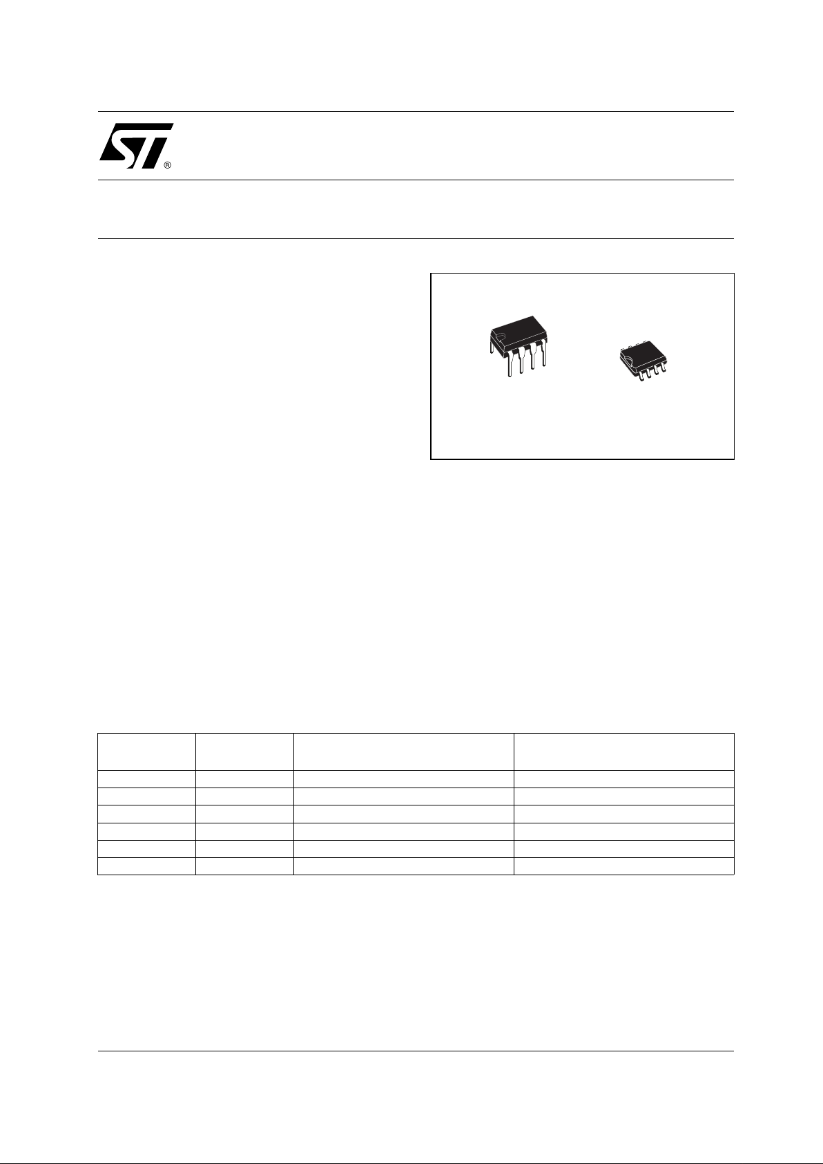
DIP SOP
Page 2
ST1480A
2/16
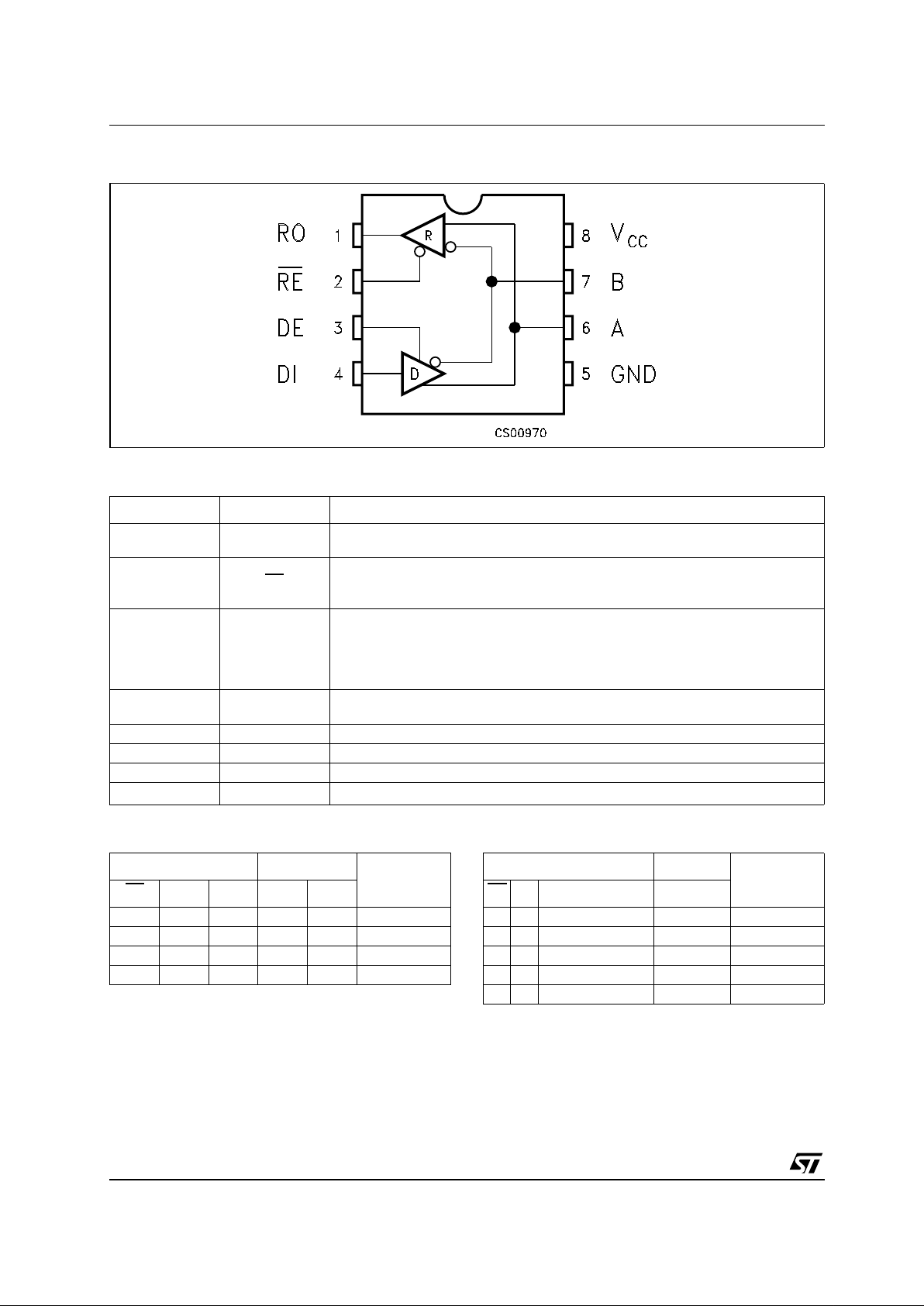
PIN CONFIGURATION
PIN DESCRIPTION
TRUTH TABLE (DRIVE R)
X= Don’t Care; Z=High Impedance
TRUTH TABLE (RECE IVER)
X= Don’t Care; Z=High Impedance
PlN N° SYMBOL NAME AND FUNCTION
1RO
Receiver Output. If A>B by 200mV, RO will be high; if A<B by 200mV, RO will be
low
2RE
Receiver Output Enable. RO is enabled when RE is low; RO is high impedance
when RE is high. If RE is high and DE is low, the device will enter a low power
shutdown mode.
3DE
Driver Output Enable. The driver outputs are enabled by bringing DE high. They
are high impedance when DE is low. If RE is high DE is low,thedevice will enter a
low-power shutdown mode. If the driver outputs are enabled, the part functions as
line driver, while they are high impedance, it functions as line receivers if RE is
low.
4DI
Driver Input. A low on DI forces output A low and output B high. Similarly, a high
on DI forces output A high and output B low
5 GND Ground
6 A Non-inverting Receiver Input and Non-inverting Driver Output
7 B Inverting Receiver Input and Inverting Driver Output
8
V
CC
Supply Voltage: VCC= 3V to 3.6V
INPUTS OUTPUTS
MODE
RE
DE DI B A
X H H L H Normal
X H L H L Normal
L L X Z Z Normal
H L X Z Z Shutdown
INPUTS OUTPUT
MODE
RE
DE A-B RO
LL ≥ -0.015V H Normal
LL ≤ -0.2V L Normal
L L Inputs Open H Normal
L L Inputs Shorted H Normal
H L X Z Shutdown
Page 3
ST1480A
3/16
ABSOLUTE MAXIMUM RATINGS
Absolute Maximum Ratings are those values beyond which damage to the device may occur. Functional operation under these condition is
not implied.
ESD PERFORMANCE: TRANSMITTER O UTPUTS, RECEIVER INPUTS
ELECTRICAL CHARACTERISTICS
V
CC
=3Vto3.6V,TA= -40 to 85°C, unless otherwise specified. Typical values are referred to TA= 25°C)
LOGIC INPUT EL ECTRICAL CHARACTERISTICS
V
CC
=3Vto3.6V,TA= -40 to 85°C, unless otherwise specified. Typical values are referred to TA= 25°C)
Symbol Parameter Value Unit
V
CC
Supply Voltage
7V
V
I
Control Input Voltage (RE,DE)
-0.3 to 7 V
V
DI
Driver Input Voltage (DI)
-0.3 to 7 V
V
DO
Driver Output Voltage (A, B)
-7.5 to 12.5 V
V
RI
Receiver Input Voltage (A, B)
-7.5 to 12.5 V
V
RO
Receiver Output Voltage (RO) -0.3 to (VCC+ 0.3)
V
Symbol Parameter Test Conditions Min. Typ. Max. Unit
ESD ESD Protection Voltage Human Body Model ± 15 KV
ESD ESD Protection Voltage IEC-1000-4-2 Contact Disharge ± 8KV
Symbol Parameter Test Conditions Min. Typ. Max. Unit
I
SUPPLYVCC
Power Supply Current No Load, DI=0V or V
CC
DE=VCC,
RE
=0V or V
CC
1.3 2.2 mA
DE=0V,
RE
=0V
1.2 1.9 mA
I
SHDN
Shutdown Supply Current DE=0V, RE=VCC, DI=0V or V
CC
0.002 1 µA
Symbol Parameter Test Conditions Min. Typ. Max. Unit
V
IL
Input Logic Threshold Low DE, DI, RE 1.3 0.8 V
V
IH
Input Logic Threshold High DE, DI, RE 2 V
I
IN1
Logic Input Current DE, DI, RE ± 2.0 µA
I
IN2
Input Current (A, B) DE=0V, VCC= 0 or 3.6V VIN=12V 1 mA
V
IN
=-7V 0.8 mA
Page 4
ST1480A
4/16
TRANSMITTER ELECTRICAL CHARACTERISTICS
V
CC
=3Vto3.6V,TA= -40 to 85°C, unless otherwise specified. T yp ical values are r efe rred to Ta=25°C)
RECEIVER ELECTRICAL CHARACTERISTICS
V
CC
=3Vto3.6V,TA= -40 to 85°C, unless otherwise specified. T yp ical values are r efe rred to Ta=25°C)
Symbol Parameter Test Conditions Min. Typ. Max. Unit
V
OD
Differential Drive Output RL= 100Ω (RS-422) (Figure 1) 2 V
R
L
=54Ω(RS-485) (Figure 1) 1.5 V
R
L
=60Ω(RS-485) (Figure 2) 1.5 V
∆V
OD
Change in magnitude of
Driver Differential Output
Voltage for Complementary
Output States (Note1)
R
L
=54Ωor 100Ω (Figure 1) 0.2 V
V
OC
Driver Common Mode
Output Voltage
RL=54Ωor 100Ω (Figure 1) 3 V
∆V
OC
Change in magnitude of
Driver Common Mode
Output Voltage (Note1)
R
L
=54Ωor 100Ω (Figure 1) 0.2 V
I
OSD
Driver Short Circuit Output
Current
± 250 mA
Symbol Parameter Test Conditions Min. Typ. Max. Unit
V
TH
Receiver Differential
Threshold Voltage
VCM= -7V to 12V, DE = 0 -0.2 -0.015 V
∆V
TH
Receiver Input Hysteresis VCM=0V 30 V
V
OH
Receiver Output High
Voltage
I
OUT
= -4mA, VID= 200mV, (Figures 8,9) 2 V
V
OL
Receiver Output Low
Voltage
I
OUT
= 4mA, VID= -200mV, (Figure 3) 0.4 V
I
OZR
3-State (High Impedance)
Output Current at Receiver
VCC= 3.6V VO=0VtoV
CC
± 1 µA
R
RIN
Receiver Input Resistance VCM= -7V to 12V 24 KΩ
I
OSR
Receiver Short-Circuit
Current
VRO=0VtoV
CC
760mA
Page 5
ST1480A
5/16
DRIVER SWITCHING CHARACTERISTICS
V
CC
=3Vto3.6V,TA= -40 to 85°C, unless otherwise specified. T yp ical values are r efe rred to Ta=25°C)
RECEIVER SWITCHING CHARACTERISTICS
V
CC
=3Vto3.6V,TA= -40 to 85°C, unless otherwise specified . Typicalvalues are referred toTa= 25°C)
Note 1:∆VODand ∆VOCare the changes in VODand VOC, respectively, when the DI input changes state.
Note 2:measuredon |t
PLH
(A)-t
PHL
(A)| and |t
PLH
(B)-t
PHL
(B)|
Note 3: The transceivers are put into shutdown by bring RE high and DE low. If the input are in state for less than 80ns, the part are guarenteed not to enter shutdown. If the inputs are in this state for at least 300ns, the parts are guarenteed to have entered shutdown.
Symbol Parameter Test Conditions Min. Typ. Max. Unit
D
R
Maximum Data Rate 12 15 Mbps
t
DD
Differential Output Delay RL=60Ω CL= 15pF, (Figures 4,5) 18 30 ns
t
TD
Differential Output
Transition Time
RL=60Ω CL= 15pF, (Figures 4,5) 12 20 ns
t
PLH
t
PHL
Propagation Delay RL=27Ω CL= 15pF, (Figures 8,9) 18 30 ns
t
PDS|tPLH -tPHL
| Propagation
Delay Skew (Note2)
RL=27Ω CL= 15pF, (Figures 8,9) 2 5 ns
t
PZL
Output Enable Time RL=110Ω (Figures 10,11) 19 35 ns
t
PZH
Output Enable Time RL=110Ω (Figures 6,7) 30 50 ns
t
PHZ
Output Disable Time RL=110Ω (Figures 6,7) 19 35 ns
t
PLZ
Output Disable Time RL=110Ω (Figures 10,11) 30 50 ns
t
SKEW
Differential Output Delay
Skew
13ns
t
ZH(SHDN)
Driver Enable from
Shutdown to Output High
30 50 ns
t
ZL(SHDN)
Driver Enable from
Shutdown to Output Low
19 35 ns
Symbol Parameter Test Conditions Min. Typ. Max. Unit
t
PLH
t
PHL
Propagation Delay VID=0Vto3VCL1= 15pF, (Figures 12,13) 30 50 ns
t
RPDS|tPLH -tPHL
| Propagation
Delay Skew
VID=0Vto3VCL1= 15pF, (Figures 12,13) 1 3 ns
t
PZL
Output Enable Time CRL= 15pF (Figures 14-18) 10 20 ns
t
PZH
Output Enable Time CRL= 15pF (Figures 14-18) 10 20 ns
t
PHZ
Output Disable Time CRL= 15pF (Figures 14-18) 10 20 ns
t
PLZ
Output Disable Time CRL= 15pF (Figures 14-18) 10 20 ns
t
ZH(SHDN)
Receiver Enable from
Shutdown to Output High
CRL= 15pF (Figures 14-18) 10 20 ns
t
ZL(SHDN)
Receiver Enable from
Shutdown to Output Low
CRL= 15pF (Figures 14-18) 20 40 ns
Page 6

ST1480A
6/16
TEST CIRCUITS AND TY PICAL CHARACTERISTICS
Figure1 : Driver and V
OC
Test Load
Figure2 : Driver V
OD
with Varying Common Mode Voltage Test Load
Figure3 : Receiver V
OH
and VOLTest Circuit
Page 7

ST1480A
7/16
Figure4 : Drive Differential Output Delay Transition Time Test Circuit
Figure5 : Drive Differential Output Delay Transition T ime Waveform
Figure6 : Drive Enable and Disable Times Test Circuit
Page 8

ST1480A
8/16
Figure7 : Drive Enable and Disable Times Waveforms
Figure8 : Drive Propagation Time Test Circuit
Figure9 : Drive Propagation Time Waveform
Page 9

ST1480A
9/16
Figure10 : Drive E nable and Disable Times Test Circuit
Figure11 : Drive E nable and Disable Times Wavef orms
Figure12 : Receiver Propagation Delay Time Test Circuit
Page 10

ST1480A
10/16
Figure13 : Receiver Propagation Delay Time Waveforms
Figure14 : Receiver Enable and Disable Times Test Circuit
Figure15 : Receiver Enable and Disable Times Waveform
Page 11

ST1480A
11/16
Figure16 : Receiver Enable and Disable Times Waveform
Figure17 : Receiver Enable and Disable Times Waveform
Figure18 : Receiver Enable and Disable Times Waveform
Page 12
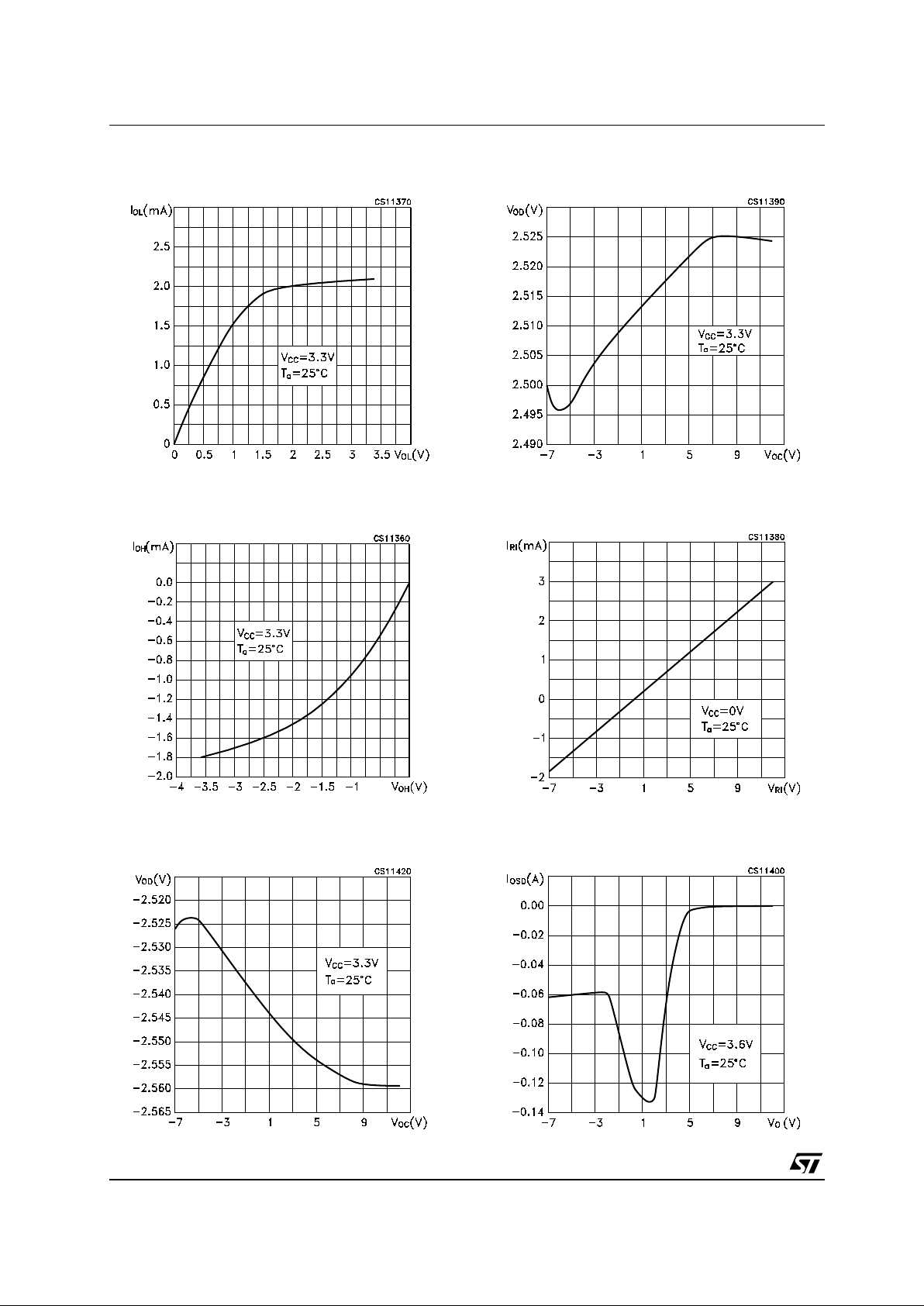
ST1480A
12/16
Figure19 : Receiver Output Current vs Output
Low Voltage
Figure20 : Receiver Output Current vs Output
High Voltage
Figure21 : Low Level Driver Output Capability
Figure22 : High Level Driver Output Capability
Figure23 : Receiver Input Characteristics
Figure24 : Driver S hort Circuit Current
Page 13

ST1480A
13/16
Figure25 : Driver S hort Circuit Current
Page 14

ST1480A
14/16
DIM.
mm. inch
MIN. TYP MAX. MIN. TYP. MAX.
A 3.3 0.130
a1 0.7 0.028
B 1.39 1.65 0.055 0.065
B1 0.91 1.04 0.036 0.041
b 0.5 0.020
b1 0.38 0.5 0.015 0.020
D 9.8 0.386
E 8.8 0.346
e 2.54 0.100
e3 7.62 0.300
e4 7.62 0.300
F 7.1 0.280
I 4.8 0.189
L 3.3 0.130
Z 0.44 1.6 0.017 0.063
Plastic DIP-8 MECHANICAL DATA
P001F
Page 15

ST1480A
15/16
DIM.
mm. inch
MIN. TYP MAX. MIN. TYP. MAX.
A 1.75 0.068
a1 0.1 0.25 0.003 0.009
a2 1.65 0.064
a3 0.65 0.85 0.025 0.033
b 0.35 0.48 0.013 0.018
b1 0.19 0.25 0.007 0.010
C 0.25 0.5 0.010 0.019
c1 45˚ (typ.)
D 4.8 5.0 0.189 0.196
E 5.8 6.2 0.228 0.244
e 1.27 0.050
e3 3.81 0.150
F 3.8 4.0 0.149 0.157
L 0.4 1.27 0.015 0. 050
M 0.6 0. 023
S
˚ (max.)
SO-8 MECHANICAL DATA
0016023
8
Page 16

ST1480A
16/16
Information furnished is believed to be accurate and reliable. However, STMicroelect ronics assum es no responsibility f or the
consequences of use of such informatio n nor for any infringement of paten ts or o ther rig hts of t hird part ies which ma y result from
its use. No license is granted by implication or otherwise under any patent or patent rights of STMicroelectronics. Specifications
mentioned in this publicatio n are subject t o change without notice. This publication supersedes and replaces all information
previousl y suppl ied. STM icroel ectronics produc ts are not auth orized for use as c ritica l compone nts in l ife s upport dev ices or
systems without express written approval of STMicroelectronics.
© The ST logo is a registered trademark of STMicroelectronics
© 2002 STMicroelectronics - Printed in Italy - All Rights Reserved
STMicroelectronics GROUP OF COMPANIES
Australia - Brazil - Canada - China - Finland - France - Germany - Hong Kong - India - Israel - Italy - Japan - Malaysia - Malta - Morocco
Singapore - Spain - Sweden - Switzerland - United Kingdom - United States.
© http://www.st.com
 Loading...