

Page 1
272-bit EEPROM with Advanced Security Mechanisms
■ 5 V Single Supply Voltage
■ Counting Capability (two options)
5
– up to 32767 (8
– 8 times reloadable, up to 4095 (8
■ Active Authentication Function (ST1335/ 1355 )
■ Cipher Block Chaining Function (ST1355)
■ Memory Divided into :
– 16 bits of Circuit Identification
– 48 bits of Card Identification
– 40 bits of Count Data
– 16 bits for Validation Cer t if ic ate
– 24 bits of Transport Code
– 64 bits of Issuer Data (ST1336) or
Authentication Secret Key (ST1335/13 55)
– 32 bits of Anti-tearing Flags (optional)
– 56 bits of User data (optionally not erasable)
■ 1 Million Erase/Write Cycle (minimum)
■ 10 Year Data Retention (minimum)
■ 3.5 ms Programming Time at 5 V (typical)
■ 500 µA Supply Current at 5 V (typical)
■ 250 µA Stand-by Current at 5 V (typical)
DESCRIPTION
The members of the ST1335/1336/1355 family are
principally designed for use in prepaid Ph onecard
applications. Each is a 272-bit EEPR OM device,
with associated security logic and special fuses to
control memory access. The m emory is a rranged
as a matrix of 34 x 8 cells, accessed in a serial bitwise fashion for reading and programming, and in
a byte-wise fashion for internal erasing. An on-chip
-1)
4
-1)
ST1335, ST1336
ST1355
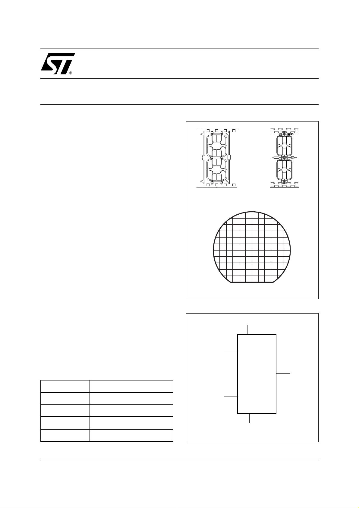
5-Contact Memory Card IC
DATA BRIEFING
(D10)
RST
1
1
Micromodule
(D15)
Wafer
V
CC
1
1
Micromodule
Figure 1. Logic Diagram
Table 1. Signal Names
CLK Clock
RST Reset
I/O Data Input / Output
V
CC
GND Ground
October 1999
Complete data available under NDA.
Supply Voltage
CLK
ST1335
ST1336
ST1355
GND
I/O
AI03106b
1/3
Page 2
ST1335, ST1336, ST1355
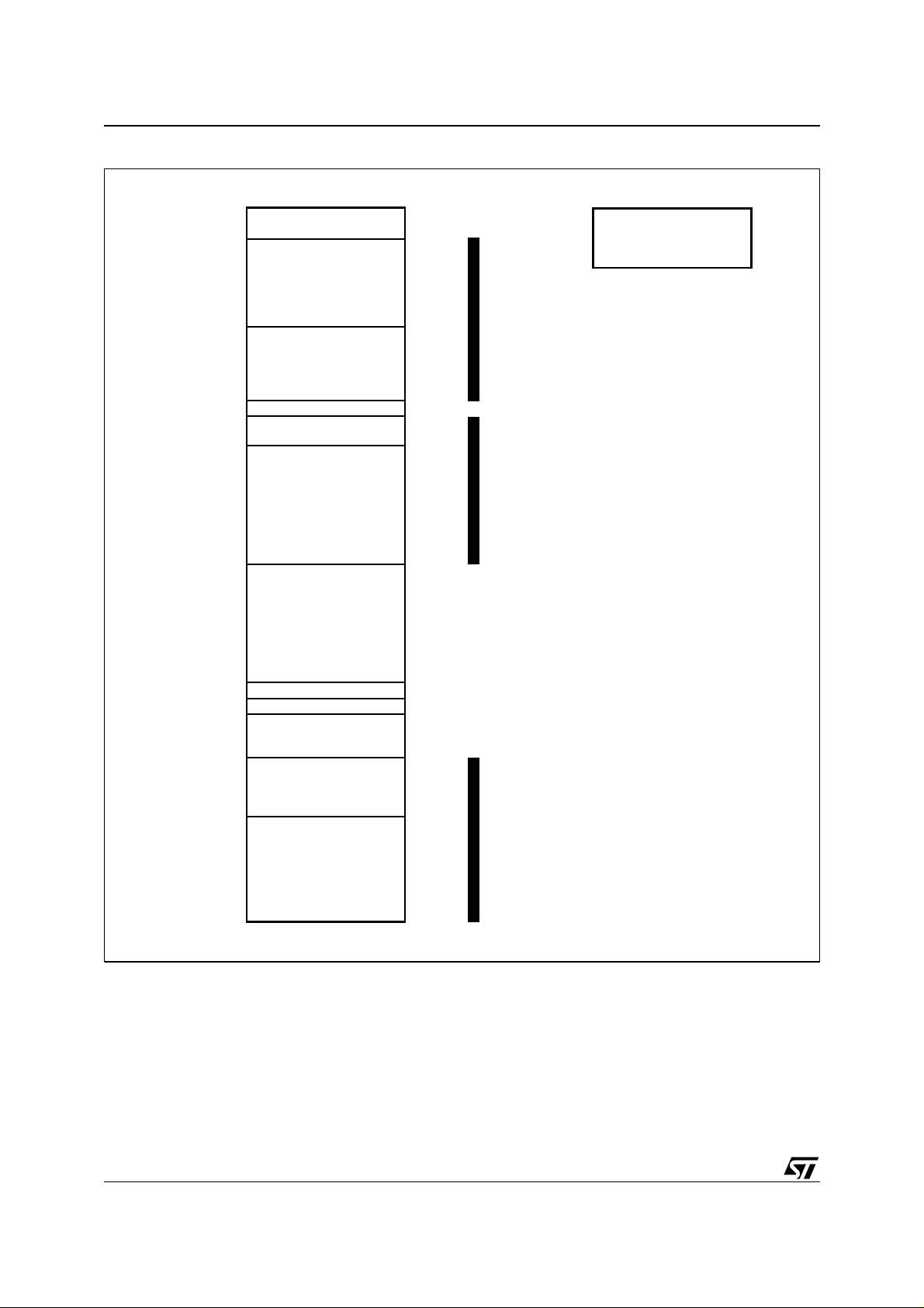
Figure 2. Me m ory Map
16 masked bits
48 bits
40 bits
8 bits
16 bits
64 bits
Circuit
Identification Area
Card Identification
Area (ID)
Data Area (CD)
(Counters and
Transport Code)
Reserved Area (RA)
Certificate (CER)
Issuer-Defined Area
(ST1336)
Authentication
Secret Key (SK)
(ST1335, ST1355)
Reserved Area
(RA)
0
16
64
104
112
128
192
32 bits
RAM1 (Write-Only)
0
(RN)
(ST1335, ST1355)
32
4 bits
4 bits
24 bits
32 bits
56 bits
Note: 1. The write-only RAM area (RN) is applicable only for the User Configuration.
Signature
Fuses
Unused
Anti-Tearing Flags
User-Defined Area
address counter provides an internal address
space of up to 512 bits.
Each member of the ST1335/1336/1355 family
has an identification data area, unit-counters (with
an anti-tearing mechanism for reliable usage in
open readers), a post validation certificate, an
issuer area (ST1336) or an aut hentication secret
256
260
264
288
320
376
Physical EEPROM CellsPhysical EEPROM CellsPhysical EEPROM Cells
key area (ST1335/1355), and a user area. This is
summarized in Figure 2.
The validation certificate allows the recognition of
the device by the appropriate security module.
The anti-tearing mechanism guards against extra,
spurious count signals being executed when the
AI03385
2/3
Page 3

ST1335, ST1336, ST1355
card is unexpectedly extracted, while an operation
is underway, in an open reader.
EXTERNAL COMMANDS
The device uses five contacts: V
, GND, I/O,
CC
CLK, RST. Four commands distinct can be
composed using these external pins:
– RESET: to reset the internal address register to
000d
– READ: to increment the internal address
register and read the data bit at the new address
– COMPARE: to allow comparison of the
presented code against the internal transport
code
– PROGRAM: to program the bit at the current
address
CONFIGURATIONS
The device works in two distinct configurations:
– Issuer Configuration: for the card manufacturer.
Customized data can be written to the chip, to
initialize it before release to the end user.
– User Configuration: for use b y the end user of
the card, but with restricted access.
OPTIONS
Three options can be chosen on ordering the
device:
– The anti-tearing mechanism can be
disconnected. In this case, the anti-tearing flag
area from bit 288d to bit 319d is unused (Figure
2).
– The user area, from bit 320d to bit 375d, can be
defined as “not erasable” in the User
Configuration.
– The reload mechanism can be activated. In this
case, erasing a bit in the reload counter
refreshes the certificate (CER). At this time, the
certificate can be programmed with a new
value.
ORDERING INFORMATION
The notation used for the device number is as
shown in Table 2. For a list of a vailable options
(speed, package, etc.) or for further information on
any aspect of this device, please contact your
nearest ST Sales Office.
Table 2. Ordering Information Scheme
Example: ST1335 –C W4 / XX YY
Product Transport Code
35 Active Authentication Function Given by ST
36 Issuer Area
55 Cipher Block Chaining
Authentication Function
Fuse Blow Voltage Delivery Form
5 V
1
1
B6 V
C
Note: 1 . Please contact your nearest ST Sales Office to check on availability
Customer Code
Given by the Issuer
Micromodule on reel
D10
Micromodule on reel
D15
W4 Wafer (180 µm thickness)
W2 Wafer (280 µm thickness)
3/3
 Loading...