

Page 1
ST13007N
HIGH VOLTAGE FAST-SWITCHING
■ HIGH VOLTAGECAPABILITY
■ NPNTRANSISTOR
■ LOW SPREAD OF DYNAMICPARAMETERS
■ MINIMUM LOT-TO-LOT SPREADFOR
RELIABLEOPERATION
■ VERYHIGH SWITCHINGSPEED
APPLICATIONS
■ ELECTRONICBALLASTSFOR
FLUORESCENT LIGHTING
■ SWITCHMODEPOWER SUPPLIES
DESCRIPTION
The device is manufactured using high voltage
Multi Epitaxial Planar technology for high
switchingspeeds and high voltagecapability.
They use a Cellular Emitter structure to enhance
switchingspeeds.
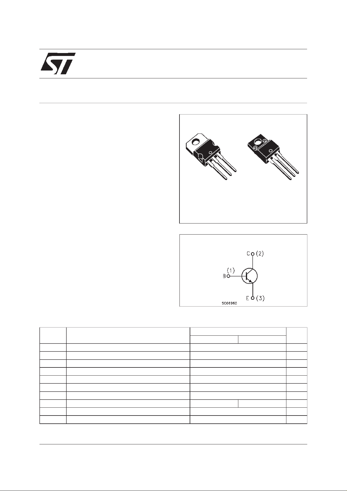
ST13007NFP
NPN POWER TRANSISTORS
3
2
1
TO-220 TO-220FP
INTERNAL SCHEMATIC DIAGRAM
3
2
1
ABSOLUTE MAXIMUM RATINGS
Symb o l Para meter Val u e Uni t
ST1 3007 N ST 13 007NFP
V
V
V
I
I
P
T
March 1999
Collector-Emitter Voltage (VBE= -1.5V) 700 V
CEV
Collector-Emitter Voltage (IB= 0 ) 400 V
CEO
Emitter-Base Voltage (IC=0) 9 V
EBO
Collector Current 8 A
I
C
Collector Peak Current 16 A
CM
Base Current 4 A
I
B
Base Peak Curre nt 8 A
BM
tot Tot al Dissip ation at T
Sto rage T emperat ure -65 to 150
stg
Max. Oper at in g Junct ion Te mperatu re 150
T
j
≤ 25oC
c
80 33 W
o
C
o
C
1/7
Page 2
ST13007N / ST13007NFP
THERMAL DATA
R
thj-case
R
thj-amb
Ther mal Resist ance Junctio n-c a se Ma x
Ther mal Resist ance Junctio n-A mbient Max
TO-220 TO - 2 20FP
1.56
62.5
3.8
62.5
o
C/W
o
C/W
ELECTRICAL CHARACTERISTICS (T
=25oC unlessotherwise specified)
case
Symbol Parameter Test Cond itions Min. Typ . Max. Unit
I
CEV
I
EBO
V
CEO(sus)
Collec t or Cut -off
Current (V
=-1.5V)
BE
Emitt er Cut-off Curren t
=0)
(I
C
∗ Co llector-Emit t er
V
=ratedV
CE
VCE=ratedV
V
=9V 1 mA
EB
CEV
CEVTc
=100oC
1
5
mA
mA
IC= 10 mA 400 V
Sust aining Voltage
∗ Collec t or-Emitter
V
CE(sat)
Saturation Voltage
V
∗ Base-Emitt er
BE(sat)
Saturation Voltage
h
∗ DC Cur r ent Gain IC=2A VCE=5V
FE
INDUCTIVE LO AD
t
* Pulsed: Pulse duration = 300µs, duty cycle 2 %
Note : Productis pre-selected inDC current gain (GROUP A and GROUP B).STMicroelectronics reserves the right to ship either groups
according to production availability. Please contact your nearest STMicroelectronics sales office for delivery details.
s
t
f
Storage Time
Fall Time
IC=2A IB=0.4A
=5A IB=1A
I
C
=8A IB=2A
I
C
=5A IB=1A Tc=100oC
I
C
IC=2A IB=0.4A
=5A IB=1A
I
C
=5A IB=1A Tc=100oC
I
C
Gr oup A
Gr oup B
=5A VCE=5V
I
C
IC = 5 A VCL=200V
=1A V
I
B1
=0Ω
R
BB
BEo f f
=-5V
15
26
5
0.6
60
1
2
3
3
1.2
1.6
1.5
28
40
30
1.5
110
V
V
V
V
V
V
V
µs
ns
2/7
Page 3
ST13007N/ ST13007NFP
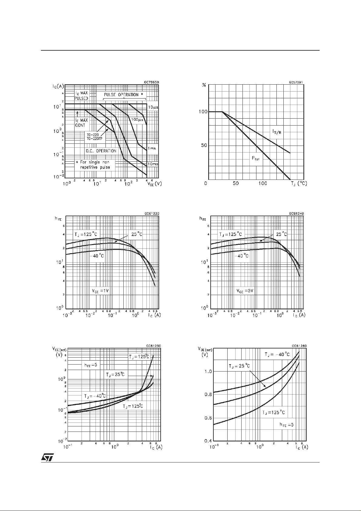
Safe OperatingAreas
DCCurrent Gain
DeratingCurve
DC Current Gain
CollectorEmitter SaturationVoltage
BaseEmitter Saturation Voltage
3/7
Page 4

ST13007N / ST13007NFP
InductiveFall Time InductiveStorage Time
ReverseBiased SOA RBSOAand InductiveLoad SwitchingTest
Circuits
4/7
1) F ast electron ic switch
2) Non- i ndu c t ive Resistor
3) Fast reco very rec tifie r
Page 5

TO-220 MECHANICAL DATA
ST13007N/ ST13007NFP
DIM.
MIN. TYP. MAX. MIN. TYP. MAX.
A 4.40 4.60 0.173 0.181
C 1.23 1.32 0.048 0.051
D 2.40 2.72 0.094 0.107
D1 1.27 0.050
E 0.49 0.70 0.019 0.027
F 0.61 0.88 0.024 0.034
F1 1.14 1.70 0.044 0.067
F2 1.14 1.70 0.044 0.067
G 4.95 5.15 0.194 0.203
G1 2.4 2.7 0.094 0.106
H2 10.0 10.40 0.393 0.409
L2 16.4 0.645
L4 13.0 14.0 0.511 0.551
L5 2.65 2.95 0.104 0.116
L6 15.25 15.75 0.600 0.620
L7 6.2 6.6 0.244 0.260
L9 3.5 3.93 0.137 0.154
DIA. 3.75 3.85 0.147 0.151
mm inch
P011C
5/7
Page 6

ST13007N / ST13007NFP
TO-220FP MECHANICAL DATA
DIM.
MIN. TYP. MAX. MIN. TYP. MAX.
A 4.4 4.6 0.173 0.181
B 2.5 2.7 0.098 0.106
D 2.5 2.75 0.098 0.108
E 0.45 0.7 0.017 0.027
F 0.75 1 0.030 0.039
F1 1.15 1.7 0.045 0.067
F2 1.15 1.7 0.045 0.067
G 4.95 5.2 0.195 0.204
G1 2.4 2.7 0.094 0.106
H 10 10.4 0.393 0.409
L2 16 0.630
L3 28.6 30.6 1.126 1.204
L4 9.8 10.6 0.385 0.417
L6 15.9 16.4 0.626 0.645
L7 9 9.3 0.354 0.366
Ø 3 3.2 0.118 0.126
mm inch
E
A
D
B
L3
L6
L7
¯
F1
F
G1
H
G
F2
123
L2
L4
6/7
Page 7

ST13007N/ ST13007NFP
Information furnished isbelieved tobe accurate and reliable. However, STMicroelectronics assumes no responsibility for theconsequences
of use of such information nor for any infringement of patents or other rights of third parties which may result from its use. No license is
granted by implication or otherwise under any patent or patent rights of STMicroelectronics. Specification mentioned in this publication are
subject tochange without notice. This publication supersedes and replaces all information previously supplied. STMicroelectronics products
are not authorized for use as critical components in life support devices or systems without express written approval of STMicroelectronics.
The ST logo is a trademark of STMicroelectronics
1999 STMicroelectronics – Printed in Italy – All Rights Reserved
STMicroelectronicsGROUP OF COMPANIES
Australia - Brazil -Canada - China - France - Germany - Italy - Japan - Korea - Malaysia - Malta - Mexico - Morocco - The Netherlands -
Singapore - Spain -Sweden - Switzerland - Taiwan - Thailand - United Kingdom - U.S.A.
http://www.st.com
.
7/7
 Loading...