

Page 1

A
8 Mbit (x16) Multi-Purpose Flash Plus
Microchip Technology Company
SST39VF801C / SST39VF802C / SST39LF801C / SST39LF802C
The SST39VF801C / SST39VF802C / SST39LF801C / SST39LF802C are 512K
x16 CMOS Multi-Purpose Flash Plus (MPF+) manufactured with SST proprietary,
high performance CMOS SuperFlash® technology. The split-gate cell design and
thick-oxide tunneling injector attain better reliability and manufacturability compared with alternate approaches. The SST39VF801C / SST39VF802C /
SST39LF801C / SST39LF802C write (Program or Erase) with a 2.7-3.6V power
supply. These devices conforms to JEDEC standard pinouts for x16 memories.
Features
• Organized as 512K x16
• Single Voltage Read and Write Operations
– 2.7-3.6V for SST39VF801C/802C
– 3.0-3.6V for SST39LF801C/802C
• Superior Reliability
– Endurance: 100,000 Cycles (Typical)
– Greater than 100 years Data Retention
• Low Power Consumption (typical values at 5 MHz)
– Active Current: 5 mA (typical)
– Standby Current: 3 µA (typical)
– Auto Low Power Mode: 3 µA (typical)
• Hardware Block-Protection/WP# Input Pin
– Top Block-Protection (top 8 KWord)
– Bottom Block-Protection (bottom 8 KWord)
• Sector-Erase Capability
– Uniform 2 KWord sectors
• Block-Erase Capability
– Flexible block architecture; one 8-, two 4-, one 16-, and
fifteen 32-KWord blocks
Data Sheet
• Security-ID Feature
– SST: 128 bits; User: 128 words
• Fast Read Access Time:
– 70 ns for SST39VF801C/802C
– 55 ns for SST39LF801C/802C
• Fast Erase and Word-Program:
– Sector-Erase Time: 18 ms (typical)
– Block-Erase Time: 18 ms (typical)
– Chip-Erase Time: 40 ms (typical)
– Word-Program Time: 7 µs (typical)
• Automatic Write Timing
– Internal VPPGeneration
• End-of-Write Detection
– Toggle Bits
– Data# Polling
– Ready/Busy# Pin
• CMOS I/O Compatibility
• JEDEC Standard
– Flash EEPROM Pinouts and command sets
• Chip-Erase Capability
• Erase-Suspend/Erase-Resume Capabilities
• Hardware Reset Pin (RST#)
• Packages Available
– 48-lead TSOP (12mm x 20mm)
– 48-ball TFBGA (6mm x 8mm)
– 48-ball WFBGA (4mm x 6mm)
• All devices are RoHS compliant
• Latched Address and Data
©2011 Silicon Storage Technology, Inc. DS25041A 05/11
www.microchip.com
Page 2

8 Mbit (x16) Multi-Purpose Flash Plus
A
Microchip Technology Company
SST39VF801C / SST39VF802C / SST39LF801C / SST39LF802C
Product Description
The SST39VF801C/802C and SST39LF801C/802C devices are 512K x16 CMOS Multi-Purpose Flash
Plus (MPF+) manufactured with SST proprietary, high performance CMOS SuperFlash technology.
The split-gate cell design and thick-oxide tunneling injector attain better reliability and manufacturability
compared with alternate approaches. The SST39VF801C/802C and SST39LF801C/802C write (Program
or Erase) with a 2.7-3.6V power supply. These devices conform to JEDEC standard pinouts for x16
memories.
Featuring high performance Word-Program, the SST39VF801C/802C and SST39LF801C/802C
devices provide a typical Word-Program time of 7 µsec. These devices use Toggle Bit, Data# Polling,
or the RY/BY# pin to indicate the completion of Program operation. To protect against inadvertent
write, they have on-chip hardware and Software Data Protection schemes. Designed, manufactured,
and tested for a wide spectrum of applications, these devices are offered with a guaranteed typical
endurance of 100,000 cycles. Data retention is rated at greater than 100 years.
The SST39VF801C/802C and SST39LF801C/802C devices are suited for applications that require
convenient and economical updating of program, configuration, or data memory. For all system applications, they significantly improve performance and reliability, while lowering power consumption. They
inherently use less energy during Erase and Program than alternative flash technologies. The total
energy consumed is a function of the applied voltage, current, and time of application. Since for any
given voltage range, the SuperFlash technology uses less current to program and has a shorter erase
time, the total energy consumed during any Erase or Program operation is less than alternative flash
technologies. These devices also improve flexibility while lowering the cost for program, data, and configuration storage applications.
Data Sheet
The SuperFlash technology provides fixed Erase and Program times, independent of the number of
Erase/Program cycles that have occurred. Therefore the system software or hardware does not have
to be modified or de-rated as is necessary with alternative flash technologies, whose Erase and Program times increase with accumulated Erase/Program cycles.
To meet high density, surface mount requirements, the SST39VF801C/802C and SST39LF801C/802C
are offered in 48-lead TSOP, 48-ball TFBGA, and 48-ball WFBGA packages. See Figures 2, 3, and 4
for pin assignments.
©2011 Silicon Storage Technology, Inc. DS25041A 05/11
2
Page 3
8 Mbit (x16) Multi-Purpose Flash Plus
A
Microchip Technology Company
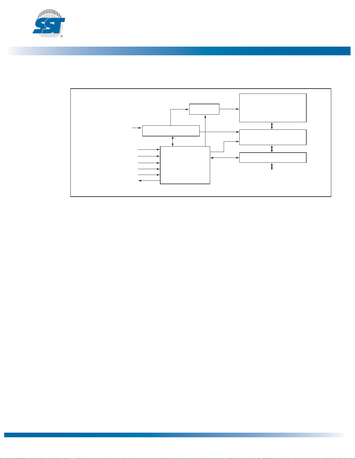
Block Diagrams
Figure 1: Functional Block Diagram
SST39VF801C / SST39VF802C / SST39LF801C / SST39LF802C
Data Sheet
SuperFlash
Memory
Y-Decoder
I/O Buffers and Data Latches
-DQ
DQ
15
0
1434 B1.0
Memory Address
RESET#
RY/BY#
CE#
OE#
WE#
WP#
X-Decoder
Address Buffer Latches
Control Logic
©2011 Silicon Storage Technology, Inc. DS25041A 05/11
3
Page 4
8 Mbit (x16) Multi-Purpose Flash Plus
A
Microchip Technology Company
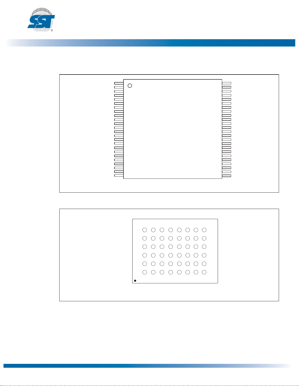
Pin Assignment
SST39VF801C / SST39VF802C / SST39LF801C / SST39LF802C
Data Sheet
A15
A14
A13
A12
A11
A10
NC
NC
WE#
RST#
NC
WP#
RY/BY#
A18
A17
1
2
3
4
5
6
A9
A8
A7
A6
A5
A4
A3
A2
A1
7
8
9
10
11
12
13
14
15
16
17
18
19
20
21
22
23
24
Standard Pinout
Top View
Die Up
48
47
46
45
44
43
42
41
40
39
38
37
36
35
34
33
32
31
30
29
28
27
26
25
A16
NC
V
SS
DQ15
DQ7
DQ14
DQ6
DQ13
DQ5
DQ12
DQ4
V
DD
DQ11
DQ3
DQ10
DQ2
DQ9
DQ1
DQ8
DQ0
OE#
V
SS
CE#
A0
Figure 2: Pin Assignments for 48-Lead TSOP
TOP VIEW (balls facing down)
6
A13
5
4
3
2
1
A9
WE#
RY/BY#
A7
A3
A12
A8
RST#
WP#
A17
A4
A14
A10
NC
A18
A6
A2
A15
A11
NC
NC
A5
A1
ABCDEFGH
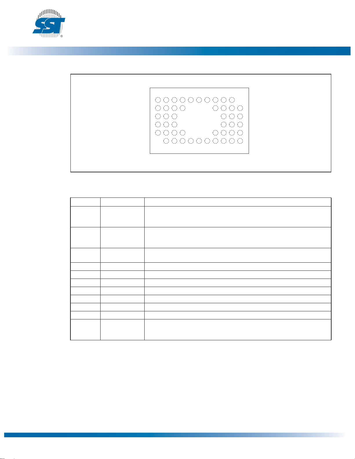
Figure 3: Pin Assignments for 48-Ball TFBGA
A16
DQ7
DQ5
DQ2
DQ0
A0
NC
DQ15
DQ14
DQ13
DQ12
V
DD
DQ10
DQ11
DQ8
DQ9
CE#
OE#
1434 48-tfbga B3K P2.0
1434 48-tsop EK P1.0
V
SS
DQ6
DQ4
DQ3
DQ1
V
SS
©2011 Silicon Storage Technology, Inc. DS25041A 05/11
4
Page 5
8 Mbit (x16) Multi-Purpose Flash Plus
A
Microchip Technology Company
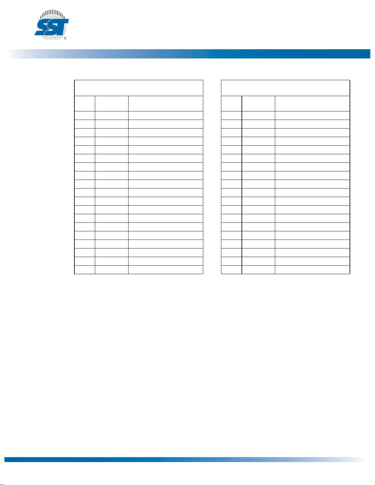
Figure 4: Pin Assignments for 48-Ball WFBGA
Table 1: Pin Description
Symbol Pin Name Functions
A
DQ
WP# Write Protect To protect the top/bottom boot block from Erase/Program operation when
RST# Reset To reset and return the device to Read mode.
CE# Chip Enable To activate the device when CE# is low.
OE# Output Enable To gate the data output buffers.
WE# Write Enable To control the Write operations.
V
V
NC No Connection Unconnected pins.
RY/BY# Ready/Busy# To output the status of a Program or Erase operation
SST39VF801C / SST39VF802C / SST39LF801C / SST39LF802C
Data Sheet
TOP VIEW (balls facing down)
6
A2
A4
A6
5
A1
4
A0
3
CE#
2
V
SS
1
A3
A5
DQ8
OE#
DQ0
A7
A18
DQ10
DQ9
DQ1
A17
WP#
NC
DQ2NCDQ3NCV
AB C D E F G H J K L
1
-A
MS
-DQ0Data Input/output To output data during Read cycles and receive input data during Write cycles.
15
DD
SS
1. AMS= Most significant address
AMS=A
Address Inputs To provide memory addresses.
0
During Sector-Erase A
During Block-Erase A
Data is internally latched during a Write cycle.
The outputs are in tri-state when OE# or CE# is high.
grounded.
Power Supply To provide power supply voltage: 2.7-3.6V
Ground
RY/BY# is a open drain output, so a 10K - 100K pull-up resistor is required
to allow RY/BY# to transition high indicating the device is ready to read.
18
WE#
RST#
A9
A11
RY/BY#
A10
A13
A14
A8
A12
A15
DQ4
DQ11
A16
NC
DQ5
DQ6
DQ7
DQ12
DQ13
DQ14
DQ15
DD
address lines will select the sector.
MS-A11
address lines will select the block.
MS-A15
V
SS
1434 48-wfbga MAQ P3.0
T1.2 25041
©2011 Silicon Storage Technology, Inc. DS25041A 05/11
5
Page 6
8 Mbit (x16) Multi-Purpose Flash Plus
A
Microchip Technology Company
Table 2: Top / Bottom Boot Block Address
SST39VF801C / SST39VF802C / SST39LF801C / SST39LF802C
Data Sheet
Top Boot Block Address
SST39VF802C/SST39LF802C
#
18 8 7E000H-7FFFFH 18 32 78000H-7FFFFH
17 4 7D000H-7DFFFH 17 32 70000H-77FFFH
16 4 7C000H-7CFFFH 16 32 68000H-6FFFFH
15 16 78000H-7BFFFH 15 32 60000H-67FFFH
14 32 70000H-77FFFH 14 32 58000H-5FFFFH
13 32 68000H-6FFFFH 13 32 50000H-57FFFH
12 32 60000H-67FFFH 12 32 48000H-4FFFFH
11 32 58000H-5FFFFH 11 32 40000H-47FFFH
10 32 50000H-57FFFH 10 32 38000H-3FFFFH
9 32 48000H-4FFFFH 9 32 30000H-37FFFH
8 32 40000H-47FFFH 8 32 28000H-2FFFFH
7 32 38000H-3FFFFH 7 32 20000H-27FFFH
6 32 30000H-37FFFH 6 32 18000H-1FFFFH
5 32 28000H-2FFFFH 5 32 10000H-17FFFH
4 32 20000H-27FFFH 4 32 08000H-0FFFFH
3 32 18000H-1FFFFH 3 16 04000H-07FFFH
2 32 10000H-17FFFH 2 4 03000H-03FFFH
1 32 08000H-0FFFFH 1 4 02000H-02FFFH
0 32 00000H-07FFFH 0 8 00000H-01FFFH
Size
(KWord)
Address Range #
Bottom Boot Block Address
SST39VF801C/SST39LF801C
Size
(KWord)
Address Range
T2.25041
©2011 Silicon Storage Technology, Inc. DS25041A 05/11
6
Page 7

8 Mbit (x16) Multi-Purpose Flash Plus
A
Microchip Technology Company
Device Operation
Commands are used to initiate the memory operation functions of the device. Commands are written
to the device using standard microprocessor write sequences. A command is written by asserting WE#
low while keeping CE# low. The address bus is latched on the falling edge of WE# or CE#, whichever
occurs last. The data bus is latched on the rising edge of WE# or CE#, whichever occurs first.
The SST39VF801C/802C and SST39LF801C/802C also have the Auto Low Power mode which puts
the device in a near standby mode after data has been accessed with a valid Read operation. This
reduces the IDDactive read current from typically 5 mA to typically 3 µA. The Auto Low Power mode
reduces the typical IDDactive read current to the range of 2 mA/MHz of Read cycle time. The device
exits the Auto Low Power mode with any address transition or control signal transition used to initiate
another Read cycle, with no access time penalty. Note that the device does not enter Auto-Low Power
mode after power-up with CE# held steadily low, until the first address transition or CE# is driven high.
Read
The Read operation of the SST39VF801C/802C and SST39LF801C/802C is controlled by CE# and OE#,
both have to be low for the system to obtain data from the outputs. CE# is used for device selection.
When CE# is high, the chip is deselected and only standby power is consumed. OE# is the output control and is used to gate data from the output pins. The data bus is in high impedance state when either
CE# or OE# is high. Refer to the Read cycle timing diagram for further details (Figure 6).
SST39VF801C / SST39VF802C / SST39LF801C / SST39LF802C
Data Sheet
Word-Program Operation
The SST39VF801C/802C and SST39LF801C/802C are programmed on a word-by-word basis. Before
programming, the sector where the word exists must be fully erased. The Program operation is accomplished in three steps. The first step is the three-byte load sequence for Software Data Protection. The
second step is to load word address and word data. During the Word-Program operation, the
addresses are latched on the falling edge of either CE# or WE#, whichever occurs last. The data is
latched on the rising edge of either CE# or WE#, whichever occurs first. The third step is the internal
Program operation which is initiated after the rising edge of the fourth WE# or CE#, whichever occurs
first. The Program operation, once initiated, will be completed within 10 µs. See Figures 7 and 8 for
WE# and CE# controlled Program operation timing diagrams and Figure 22 for flowcharts. During the
Program operation, the only valid reads are Data# Polling and Toggle Bit. During the internal Program
operation, the host is free to perform additional tasks. Any commands issued during the internal Program operation are ignored. During the command sequence, WP# should be statically held high or low.
Sector/Block-Erase Operation
The Sector- (or Block-) Erase operation allows the system to erase the device on a sector-by-sector (or
block-by-block) basis. The SST39VF801C/802C and SST39LF801C/802C offer both Sector-Erase and
Block-Erase mode.
The sector architecture is based on a uniform sector size of 2 KWord. The Block-Erase mode is based
on non-uniform block sizes—fifteen 32 KWord, one 16 KWord, two 4 KWord, and one 8 KWord blocks.
See Figure 2 for top and bottom boot device block addresses. The Sector-Erase operation is initiated
by executing a six-byte command sequence with Sector-Erase command (50H) and sector address
(SA) in the last bus cycle. The Block-Erase operation is initiated by executing a six-byte command
sequence with Block-Erase command (30H) and block address (BA) in the last bus cycle. The sector
or block address is latched on the falling edge of the sixth WE# pulse, while the command (30H or
50H) is latched on the rising edge of the sixth WE# pulse. The internal Erase operation begins after the
©2011 Silicon Storage Technology, Inc. DS25041A 05/11
7
Page 8

8 Mbit (x16) Multi-Purpose Flash Plus
A
Microchip Technology Company
sixth WE# pulse. The End-of-Erase operation can be determined using either Data# Polling or Toggle
Bit methods. See Figures 12 and 13 for timing waveforms and Figure 26 for the flowchart. Any commands issued during the Sector- or Block-Erase operation are ignored. When WP# is low, any attempt
to Sector- (Block-) Erase the protected block will be ignored. During the command sequence, WP#
should be statically held high or low.
Erase-Suspend/Erase-Resume Commands
The Erase-Suspend operation temporarily suspends a Sector- or Block-Erase operation thus allowing
data to be read from any memory location, or program data into any sector/block that is not suspended
for an Erase operation. The operation is executed by issuing one byte command sequence with EraseSuspend command (B0H). The device automatically enters read mode typically within 20 µs after the
Erase-Suspend command had been issued. Valid data can be read from any sector or block that is not
suspended from an Erase operation. Reading at address location within erase-suspended sectors/
blocks will output DQ2toggling and DQ6at ‘1’. While in Erase-Suspend mode, a Word-Program operation is allowed except for the sector or block selected for Erase-Suspend.
To resume Sector-Erase or Block-Erase operation which has been suspended the system must issue
Erase Resume command. The operation is executed by issuing one byte command sequence with
Erase Resume command (30H) at any address in the last Byte sequence.
SST39VF801C / SST39VF802C / SST39LF801C / SST39LF802C
Data Sheet
Chip-Erase Operation
The SST39VF801C/802C and SST39LF801C/802C provide a Chip-Erase operation, which allows the
user to erase the entire memory array to the ‘1’ state. This is useful when the entire device must be
quickly erased.
The Chip-Erase operation is initiated by executing a six-byte command sequence with Chip-Erase
command (10H) at address 555H in the last byte sequence. The Erase operation begins with the rising
edge of the sixth WE# or CE#, whichever occurs first. During the Erase operation, the only valid read is
Toggle Bit or Data# Polling. See Table 7 for the command sequence, Figure 11 for timing diagram, and
Figure 26 for the flowchart. Any commands issued during the Chip-Erase operation are ignored. When
WP# is low, any attempt to Chip-Erase will be ignored. During the command sequence, WP# should
be statically held high or low.
Write Operation Status Detection
The SST39VF801C/802C and SST39LF801C/802C provide two software means to detect the completion of a Write (Program or Erase) cycle, in order to optimize the system write cycle time. The software
detection includes two status bits: Data# Polling (DQ7) and Toggle Bit (DQ6). The End-of-Write detection mode is enabled after the rising edge of WE#, which initiates the internal Program or Erase operation.
The actual completion of the nonvolatile write is asynchronous with the system; therefore, either a
Data# Polling or Toggle Bit read may be simultaneous with the completion of the write cycle. If this
occurs, the system may possibly get an erroneous result, i.e., valid data may appear to conflict with
either DQ7or DQ6. In order to prevent spurious rejection, if an erroneous result occurs, the software
routine should include a loop to read the accessed location an additional two (2) times. If both reads
are valid, then the device has completed the Write cycle, otherwise the rejection is valid.
©2011 Silicon Storage Technology, Inc. DS25041A 05/11
8
Page 9

8 Mbit (x16) Multi-Purpose Flash Plus
A
Microchip Technology Company
Ready/Busy# (RY/BY#)
The devices include a Ready/Busy# (RY/BY#) output signal. RY/BY# is an open drain output pin that
indicates whether an Erase or Program operation is in progress. Since RY/BY# is an open drain output, it allows several devices to be tied in parallel to VDDvia an external pull-up resistor. After the rising
edge of the final WE# pulse in the command sequence, the RY/BY# status is valid.
When RY/BY# is actively pulled low, it indicates that an Erase or Program operation is in progress.
When RY/BY# is high (Ready), the devices may be read or left in standby mode.
Data# Polling (DQ7)
When the SST39VF801C/802C and SST39LF801C/802C are in the internal Program operation, any
attempt to read DQ7will produce the complement of the true data. Once the Program operation is
completed, DQ7will produce true data. Note that even though DQ7may have valid data immediately following the completion of an internal Write operation, the remaining data outputs may still be invalid: valid data on
the entire data bus will appear in subsequent successive Read cycles after an interval of 1 µs. During internal
Erase operation, any attempt to read DQ7will produce a ‘0’. Once the internal Erase operation is completed, DQ7will produce a ‘1’. The Data# Polling is valid after the rising edge of fourth WE# (or CE#)
pulse for Program operation. For Sector-, Block- or Chip-Erase, the Data# Polling is valid after the rising edge of sixth WE# (or CE#) pulse. See Figure 9 for Data# Polling timing diagram and Figure 23 for
a flowchart.
SST39VF801C / SST39VF802C / SST39LF801C / SST39LF802C
Data Sheet
Toggle Bits (DQ6 and DQ2)
During the internal Program or Erase operation, any consecutive attempts to read DQ6will produce
alternating ‘1’s and ‘0’s, i.e., toggling between 1 and 0. When the internal Program or Erase operation
is completed, the DQ6bit will stop toggling. The device is then ready for the next operation. For Sector, Block-, or Chip-Erase, the toggle bit (DQ6) is valid after the rising edge of sixth WE# (or CE#) pulse.
DQ6will be set to ‘1’ if a Read operation is attempted on an Erase-Suspended Sector/Block. If Program operation is initiated in a sector/block not selected in Erase-Suspend mode, DQ6will toggle.
An additional Toggle Bit is available on DQ2, which can be used in conjunction with DQ6to check
whether a particular sector is being actively erased or erase-suspended. Table 3 shows detailed status
bits information. The Toggle Bit (DQ2) is valid after the rising edge of the last WE# (or CE#) pulse of
Write operation. See Figure 10 for Toggle Bit timing diagram and Figure 23 for a flowchart.
Table 3: Write Operation Status
Status DQ
Normal Operation Standard Program DQ
Standard Erase 0 Toggle Toggle 0
Erase-Suspend
Mode
Note: DQ7and DQ2require a valid address when reading status information.
Read from Erase-Suspended Sector/Block
Read from Non-EraseSuspended Sector/Block
Program DQ
7
# Toggle No Toggle 0
7
1 1 Toggle 1
Data Data Data 1
# Toggle N/A 0
7
DQ
6
DQ
2
RY/BY#
T3.0 25041
©2011 Silicon Storage Technology, Inc. DS25041A 05/11
9
Page 10
8 Mbit (x16) Multi-Purpose Flash Plus
A
Microchip Technology Company
Data Protection
The SST39VF801C/802C and SST39LF801C/802C provide both hardware and software features to protect nonvolatile data from inadvertent writes.
Hardware Data Protection
Noise/Glitch Protection: A WE# or CE# pulse of less than 5 ns will not initiate a write cycle.
VDDPower Up/Down Detection: The Write operation is inhibited when VDDis less than 1.5V.
Write Inhibit Mode: Forcing OE# low, CE# high, or WE# high will inhibit the Write operation. This prevents inadvertent writes during power-up or power-down.
Hardware Block Protection
The SST39VF802C/SST39LF802C support top hardware block protection, which protects the top 8
KWord block of the device. The SST39VF801C/SST39LF801C support bottom hardware block protection, which protects the bottom 8KWord block of the device. The Boot Block address ranges are
described in Table 4. Program and Erase operations are prevented on the 8 KWord when WP# is low.
If WP# is left floating, it is internally held high via a pull-up resistor, and the Boot Block is unprotected,
enabling Program and Erase operations on that block.
SST39VF801C / SST39VF802C / SST39LF801C / SST39LF802C
Data Sheet
Table 4: Boot Block Address Ranges
Product Address Range
Bottom Boot Block
SST39VF801C/SST39LF801C 00000H - 01FFFH
Top Boot Block
SST39VF802C/SST39LF802C 7E000H - 7FFFFH
Hardware Reset (RST#)
The RST# pin provides a hardware method of resetting the device to read array data. When the RST#
pin is held low for at least T
no internal Program/Erase operation is in progress, a minimum period of T
is driven high before a valid Read can take place (see Figure 18).
The Erase or Program operation that has been interrupted needs to be re-initiated after the device
resumes normal operation mode to ensure data integrity.
any in-progress operation will terminate and return to Read mode. When
RP,
Software Data Protection (SDP)
The SST39VF801C/802C and SST39LF801C/802C provide the JEDEC approved Software Data Protection scheme for all data alteration operations, i.e., Program and Erase. Any Program operation
requires the inclusion of the three-byte sequence. The three-byte load sequence is used to initiate the
Program operation, providing optimal protection from inadvertent Write operations, e.g., during the
system power-up or power-down. Any Erase operation requires the inclusion of six-byte sequence.
These devices are shipped with the Software Data Protection permanently enabled. See Table 7 for
is required after RST#
RHR
T4.0 25041
©2011 Silicon Storage Technology, Inc. DS25041A 05/11
10
Page 11
8 Mbit (x16) Multi-Purpose Flash Plus
A
Microchip Technology Company
the specific software command codes. During SDP command sequence, invalid commands will abort
the device to read mode within T
during any SDP command sequence.
Common Flash Memory Interface (CFI)
The SST39VF801C/802C and SST39LF801C/802C also contain the CFI information to describe the
characteristics of the device. In order to enter the CFI Query mode, the system writes a three-byte
sequence, same as product ID entry command with 98H (CFI Query command) to address 555H in
the last byte sequence. Additionally, the system can use the one-byte sequence with 55H on the
Address and 89H on the Data Bus to enter the CFI Query mode. Once the device enters the CFI
Query mode, the system can read CFI data at the addresses given in Tables 8 through 10. The system
must write the CFI Exit command to return to Read mode from the CFI Query mode.
Product Identification
The Product Identification mode identifies the devices as the SST39VF801C / SST39VF802C /
SST39LF801C / SST39LF802C, and manufacturer as SST. This mode may be accessed software
operations. Users may use the Software Product Identification operation to identify the part (i.e., using
the device ID) when using multiple manufacturers in the same socket. For details, see Table 7 for software operation, Figure 14 for the Software ID Entry and Read timing diagram and Figure 24 for the
Software ID Entry command sequence flowchart.
SST39VF801C / SST39VF802C / SST39LF801C / SST39LF802C
Data Sheet
The contents of DQ15-DQ8can be VILor VIH, but no other value,
RC.
Table 5: Product Identification
Manufacturer’s ID 0000H BFH
Device ID
SST39VF801C/SST39LF801C 0001H 233BH
SST39VF802C/SST39LF802C 0001H 233AH
Product Identification Mode Exit/CFI Mode Exit
In order to return to the standard Read mode, the Software Product Identification mode must be exited.
Exit is accomplished by issuing the Software ID Exit command sequence, which returns the device to
the Read mode. This command may also be used to reset the device to the Read mode after any inadvertent transient condition that apparently causes the device to behave abnormally, e.g., not read correctly. Please note that the Software ID Exit/CFI Exit command is ignored during an internal Program
or Erase operation. See Table 7 for software command codes, Figure 16 for timing waveform, and Figure 25 for flowcharts.
Address Data
T5.2 25041
©2011 Silicon Storage Technology, Inc. DS25041A 05/11
11
Page 12

8 Mbit (x16) Multi-Purpose Flash Plus
A
Microchip Technology Company
Security ID
The SST39VF801C/802C and SST39LF801C/802C devices offer a 136 Word Security ID space. The
Secure ID space is divided into two segments—one factory programmed segment and one user programmed segment. The first segment is programmed and locked at SST with a random 128-bit number. The user segment, with a 128 word space, is left un-programmed for the customer to program as
desired.
To program the user segment of the Security ID, the user must use the Security ID Word-Program
command. To detect end-of-write for the SEC ID, read the toggle bits. Do not use Data# Polling. Once
this is complete, the Sec ID should be locked using the User Sec ID Program Lock-Out. This disables
any future corruption of this space. Note that regardless of whether or not the Sec ID is locked, neither
Sec ID segment can be erased.
The Secure ID space can be queried by executing a three-byte command sequence with Enter Sec ID
command (88H) at address 555H in the last byte sequence. To exit this mode, the Exit Sec ID command should be executed. Refer to Table 7 for more details.
SST39VF801C / SST39VF802C / SST39LF801C / SST39LF802C
Data Sheet
©2011 Silicon Storage Technology, Inc. DS25041A 05/11
12
Page 13

8 Mbit (x16) Multi-Purpose Flash Plus
A
Microchip Technology Company
Operations
Table 6: Operation Modes Selection
Mode CE# OE# WE# DQ Address
Read V
Program V
Erase V
Standby V
Write Inhibit X V
Product Identification
Software Mode V
Table 7: Software Command Sequence
Command
Sequence
Word-Program
Sector-Erase
Block-Erase
Chip-Erase
Erase-Suspend
Erase-Resume
Query Sec ID
User Security ID
Word-Program
User Security ID
Program LockOut
Software ID
Entry
CFI Query Entry
CFI Query Entry
Software ID Exit
/CFI Exit/Sec ID
Exit
Software ID Exit
/CFI Exit/Sec ID
Exit
SST39VF801C / SST39VF802C / SST39LF801C / SST39LF802C
Data Sheet
V
IL
IL
IL
IH
IL
V
IH
V
IH
X X High Z X
IL
XXV
V
IL
1. X can be VILor VIH, but no other value.
IL
1st Bus
Write Cycle
Addr
1
Data
2
Addr1Data2Addr1Data2Addr1Data2Addr1Data2Addr1Data
555H AAH 2AAH 55H 555H A0H WA
555H AAH 2AAH 55H 555H 80H 555H AAH 2AAH 55H SA
555H AAH 2AAH 55H 555H 80H 555H AAH 2AAH 55H BA
555H AAH 2AAH 55H 555H 80H 555H AAH 2AAH 55H 555H 10H
XXXH B0H
XXXH 30H
5
555H AAH 2AAH 55H 555H 88H
555H AAH 2AAH 55H 555H A5H WA6Data
555H AAH 2AAH 55H 555H 85H XXH60000
7,8
555H AAH 2AAH 55H 555H 90H
555H AAH 2AAH 55H 555H 98H
55H 98H
9,10
555H AAH 2AAH 55H 555H F0H
9,10
XXH F0H
1. Address format A10-A0(Hex). Addresses A11-A18can be VILor VIH, but no other value, for Command sequence.
2. DQ15-DQ8can be VILor VIH, but no other value, for Command sequence
3. WA = Program Word address
4. SAXfor Sector-Erase; uses AMS-A11address lines
BAX, for Block-Erase; uses AMS-A15address lines
AMS= Most significant address; AMS=A
V
IH
V
IL
V
IL
X High Z/ D
IH
V
IH
2nd Bus
Write Cycle
18
D
OUT
D
IN
1
X
High Z/ D
3rd Bus
Write Cycle
OUT
OUT
A
IN
A
IN
Sector or block address, XXH for ChipErase
X
X
See Table 7
4th Bus
Write Cycle
3
Data
5th Bus
Write Cycle
Write Cycle
H
T6.0 25041
6th Bus
4
X
4
X
2
50H
30H
T7.6 25041
©2011 Silicon Storage Technology, Inc. DS25041A 05/11
13
Page 14

8 Mbit (x16) Multi-Purpose Flash Plus
A
Microchip Technology Company
Table 8: CFI Query Identification String
SST39VF801C / SST39VF802C / SST39LF801C / SST39LF802C
Data Sheet
5. With AMS-A4= 0; Sec ID is read with A3-A0,
SST ID is read with A3= 0 (Address range = 000000H to 000007H),
User ID is read with A3= 1 (Address range = 000008H to 000087H).
Lock Status is read with A7-A0= 0000FFH. Unlocked: DQ3= 1 / Locked: DQ3=0.
6. Valid Word-Addresses for Sec ID are from 000000H-000007H and 000008H-000087H.
7. The device does not remain in Software Product ID Mode if powered down.
8. With AMS-A1=0; SST Manufacturer ID = 00BFH, is read with A0=0,
SST39VF801C/SST39LF801C Device ID = 233BH, is read with A0= 1, SST39VF802C/SST39LF802C Device ID =
233AH, is read with A0=1,
AMS= Most significant address; AMS=A
9. Both Software ID Exit operations are equivalent
10. If users never lock after programming, Sec ID can be programmed over the previously unprogrammed bits (data=1)
using the Sec ID mode again (the programmed ‘0’ bits cannot be reversed to ‘1’). Valid Word-Addresses for Sec ID are
from 000000H-000007H and 000008H-000087H.
Address Data Data
10H 0051H Query Unique ASCII string “QRY”
11H 0052H
12H 0059H
13H 0002H Primary OEM command set
14H 0000H
15H 0000H Address for Primary Extended Table
16H 0000H
17H 0000H Alternate OEM command set (00H = none exists)
18H 0000H
19H 0000H Address for Alternate OEM extended Table (00H = none exits)
1AH 0000H
1. Refer to CFI publication 100 for more details.
18
1
T8.1 25041
Table 9: System Interface Information
Address Data Data
1BH 0027H V
1CH 0036H V
1DH 0000H V
1EH 0000H V
1FH 0003H Typical time out for Word-Program 2
20H 0000H Typical time out for min. size buffer program 2
21H 0004H Typical time out for individual Sector/Block-Erase 2
22H 0005H Typical time out for Chip-Erase 2
23H 0001H Maximum time out for Word-Program 2
24H 0000H Maximum time out for buffer program 2
25H 0001H Maximum time out for individual Sector/Block-Erase 2
26H 0001H Maximum time out for Chip-Erase 2
©2011 Silicon Storage Technology, Inc. DS25041A 05/11
Min (Program/Erase)
DD
-DQ4: Volts, DQ3-DQ0: 100 millivolts
DQ
7
Max (Program/Erase)
DD
DQ
-DQ4: Volts, DQ3-DQ0: 100 millivolts
7
min. (00H = no VPPpin)
PP
max. (00H = no VPPpin)
PP
14
N
µs (23= 8 µs)
N
µs (00H = not supported)
N
ms (24=16ms)
N
ms (25=32ms)
N
times typical (21x23=16µs)
N
times typical
N
times typical (21x24=32ms)
N
times typical (21x25=64ms)
T9.3 25041
Page 15

8 Mbit (x16) Multi-Purpose Flash Plus
A
Microchip Technology Company
Table 10:Device Geometry Information
Address Data Data
SST39VF801C / SST39VF802C / SST39LF801C / SST39LF802C
Data Sheet
N
27H 0014H Device size = 2
28H 0001H Flash Device Interface description; 0001H = x16-only asynchronous interface
29H 0000H
2AH 0000H Maximum number of byte in multi-byte write = 2
2BH 0000H
2CH 0005H Number of Erase Sector/Block sizes supported by device
2DH 0000H Erase Block Region 1 Information (Refer to the CFI specification or CFI publication
2EH 0000H
2FH 0040H
30H 0000H
31H 0001H Erase Block Region 2 Information
32H 0000H
33H 0020H
34H 0000H
35H 0000H Erase Block Region 3 Information
36H 0000H
37H 0080H
38H 0000H
39H 000FH Erase Block Region 4 Information
3AH 0000H
3BH 0000H
3CH 0001H
100)
Bytes (14H = 20; 220= 1 MByte)
N
(00H = not supported)
T10.0 25041
©2011 Silicon Storage Technology, Inc. DS25041A 05/11
15
Page 16

8 Mbit (x16) Multi-Purpose Flash Plus
A
Microchip Technology Company
SST39VF801C / SST39VF802C / SST39LF801C / SST39LF802C
Electrical Specifications
Absolute Maximum Stress Ratings (Applied conditions greater than those listed under “Absolute
Maximum Stress Ratings” may cause permanent damage to the device. This is a stress rating only and
functional operation of the device at these conditions or conditions greater than those defined in the
operational sections of this data sheet is not implied. Exposure to absolute maximum stress rating conditions may affect device reliability.)
Temperature Under Bias ............................................. -55°C to +125°C
Storage Temperature ................................................ -65°C to +150°C
D. C. Voltage on Any Pin to Ground Potential ............................-0.5V to VDD+0.5V
Transient Voltage (<20 ns) on Any Pin to Ground Potential ..................-2.0V to VDD+2.0V
Voltage on A9Pin to Ground Potential .....................................-0.5V to 13.2V
Package Power Dissipation Capability (TA= 25°C) .................................. 1.0W
Surface Mount Solder Reflow ...................................... 260°C for 10 seconds
Output Short Circuit Current1.................................................. 50mA
1. Outputs shorted for no more than one second. No more than one output shorted at a time.
Table 11:Operating Range
Range Ambient Temp V
Commercial 0°C to +70°C 2.7-3.6V
Industrial -40°C to +85°C 2.7-3.6V
Data Sheet
DD
T11.0 25041
Table 12:AC Conditions of Test
Input Rise/Fall Time Output Load
5ns C
1. See Figures 20 and 21
1
=30pF
L
T12.1 25041
©2011 Silicon Storage Technology, Inc. DS25041A 05/11
16
Page 17

8 Mbit (x16) Multi-Purpose Flash Plus
A
Microchip Technology Company
Power Up Specifications
All functionalities and DC specifications are specified for a VDDramp rate of greater than 1V per 100
ms (0V to 3V in less than 300 ms). If the VDD ramp rate is slower than 1V per 100 ms, a hardware
reset is required. The recommended VDDpower-up to RESET# high time should be greater than 100
µs to ensure a proper reset.
Figure 5: Power-Up Diagram
SST39VF801C / SST39VF802C / SST39LF801C / SST39LF802C
Data Sheet
100µs
V
IH
T
5 0ns
RHR
1434 F24.0
V
DD
RESET#
CE#
VDDmin
0V
T
PU-READ
Table 13:DC Operating Characteristics V
= 2.7-3.6V
DD
1
Limits
Symbol Parameter
I
DD
Power Supply Current Address input=V
3
Read
Program and Erase 30 mA CE#=WE#=VIL, OE#=V
I
I
I
I
SB
ALP
LI
LIW
Standby VDDCurrent 20 µA CE#=V
Auto Low Power 20 µA CE#=V
Input Leakage Current 1 µA VIN=GND to VDD,VDD=VDDMax
Input Leakage Current
18 mA CE#=VIL, OE#=WE#=VIH, all I/Os open
10 µA WP#=GND to VDDor RST#=GND to V
Test ConditionsMin Max Units
V
DD=VDD
RST#=V
WE#=V
Max
IHC,VDD=VDD
DD
DD
ILC,VDD=VDD
All inputs=V
2
ILT/VIHT
IH
Max
±0.3, WP#=VDD±0.3,
±0.3
Max
SS
or V
DD,
WE#=V
on WP# pin and RST#
I
LO
V
IL
V
ILC
V
IH
V
IHC
V
OL
V
OH
1. Typical conditions for the Active Current shown on the front page of the data sheet are average values at 25°C
2. See Figure 20
3. The IDDcurrent listed is typically less than 2mA/MHz, with OE# at V
Output Leakage Current 10 µA V
=GND to VDD,VDD=VDDMax
OUT
Input Low Voltage 0.8 V VDD=VDDMin
Input Low Voltage (CMOS) 0.3 V VDD=VDDMax
Input High Voltage 0.7V
DDVDD
+0.3 V VDD=VDDMax
Input High Voltage (CMOS) VDD-0.3 VDD+0.3 V VDD=VDDMax
Output Low Voltage 0.2 V IOL=100 µA, VDD=VDDMin
Output High Voltage VDD-0.2 V IOH=-100 µA, VDD=VDDMin
(room temperature), and VDD= 3V. Not 100% tested.
Typical VDDis 3V.
IH.
, at f=5 MHz,
IHC
DD
T13.8 25041
©2011 Silicon Storage Technology, Inc. DS25041A 05/11
17
Page 18

8 Mbit (x16) Multi-Purpose Flash Plus
A
Microchip Technology Company
Table 14:Recommended System Power-up Timings
Symbol Parameter Minimum Units
T
T
Table 15:Capacitance (T
Parameter Description Test Condition Maximum
C
C
Table 16:Reliability Characteristics
Symbol Parameter Minimum Specification Units Test Method
N
T
I
LTH
SST39VF801C / SST39VF802C / SST39LF801C / SST39LF802C
Data Sheet
1
PU-READ
PU-WRITE
1. This parameter is measured only for initial qualification and after a design or process change that could affect this
parameter.
1
I/O
1
IN
1. This parameter is measured only for initial qualification and after a design or process change that could affect this
parameter.
1,2
END
1
DR
1
1. This parameter is measured only for initial qualification and after a design or process change that could affect this
parameter.
2. N
END
result in a higher minimum specification.
Power-up to Read Operation 100 µs
1
Power-up to Program/Erase Operation 100 µs
= 25°C, f=1 Mhz, other pins open)
A
I/O Pin Capacitance V
=0V 12pF
I/O
Input Capacitance VIN=0V 6pF
Endurance 10,000 Cycles JEDEC Standard A117
Data Retention 100 Years JEDEC Standard A103
Latch Up 100 + I
endurance rating is qualified as a 10,000 cycle minimum for the whole device. A sector- or block-level rating would
DD
mA JEDEC Standard 78
T14.0 25041
T15.0 25041
T16.2 25041
©2011 Silicon Storage Technology, Inc. DS25041A 05/11
18
Page 19

8 Mbit (x16) Multi-Purpose Flash Plus
A
Microchip Technology Company
SST39VF801C / SST39VF802C / SST39LF801C / SST39LF802C
AC Characteristics
Table 17:Read Cycle Timing Parameters VDD= 2.7-3.6V
Symbol Parameter
T
RC
T
CE
T
AA
T
OE
1
T
CLZ
1
T
OLZ
1
T
CHZ
1
T
OHZ
1
T
OH
1
T
RP
1
T
RHR
1,2
T
RY
1. This parameter is measured only for initial qualification and after a design or process change that could affect this parameter.
2. This parameter applies to Sector-Erase, Block-Erase and Program operations.
This parameter does not apply to Chip-Erase operations.
Data Sheet
SST39VF801C/802C SST39LF801C/802C
UnitsMin Max Min Max
Read Cycle Time 70 55 ns
Chip Enable Access Time 70 55 ns
Address Access Time 70 55 ns
Output Enable Access Time 35 30 ns
CE# Low to Active Output 0 0 ns
OE# Low to Active Output 0 0 ns
CE# High to High-Z Output 20 15 ns
OE# High to High-Z Output 20 15 ns
Output Hold from Address Change 0 0 ns
RST# Pulse Width 500 500 ns
RST# High before Read 50 50 ns
RST# Pin Low to Read Mode 20 20 µs
T17.3 25041
Table 18:Program/Erase Cycle Timing Parameters
Symbol Parameter Min Max Units
T
BP
T
AS
T
AH
T
CS
T
CH
T
OES
T
OEH
T
CP
T
WP
T
WPH
1
T
CPH
T
DS
1
T
DH
1
T
IDA
T
SE
T
BE
T
SCE
1,2
T
BY
1
T
BR
1. This parameter is measured only for initial qualification and after a design or process change that could affect this parameter.
2. This parameter applies to Sector-Erase, Block-Erase, and Program operations.
Word-Program Time 10 µs
Address Setup Time 0 ns
Address Hold Time 30 ns
WE# and CE# Setup Time 0 ns
WE# and CE# Hold Time 0 ns
OE# High Setup Time 0 ns
OE# High Hold Time 10 ns
CE# Pulse Width 40 ns
WE# Pulse Width 40 ns
1
WE# Pulse Width High 30 ns
CE# Pulse Width High 30 ns
Data Setup Time 30 ns
Data Hold Time 0 ns
Software ID Access and Exit Time 150 ns
Sector-Erase 25 ms
Block-Erase 25 ms
Chip-Erase 50 ms
RY/BY# Delay Time 90 ns
Bus Recovery Time 0 µs
T18.1 25041
©2011 Silicon Storage Technology, Inc. DS25041A 05/11
19
Page 20

8 Mbit (x16) Multi-Purpose Flash Plus
A
Microchip Technology Company
ADDRESS A
SST39VF801C / SST39VF802C / SST39LF801C / SST39LF802C
Data Sheet
MS-0
CE#
OE#
V
IH
WE#
HIGH-Z
DQ
15-0
Note: AMS= Most significant address
AMS=A
18
T
OLZ
T
CLZ
T
RC
T
CE
T
OE
T
AA
T
OHZ
T
T
OH
CHZ
HIGH-Z
DATA VALIDDATA VALID
1434 F03.0
Figure 6: Read Cycle Timing Diagram
ADDRESSES
WE#
T
AS
OE#
CE#
RY/BY#
DQ
15-0
Note: WP# must be held in proper logic state (V
or VIH) 1µs prior to and 1µs after the command sequence.
X can be VILor VIH, but no other value.
555 2AA 555 ADDR
T
AH
T
WP
T
WPH
T
CS
XXAA XX55 XXA0 DATA
IL
T
CH
T
DS
WORD
(ADDR/DATA)
T
BP
T
BY
T
DH
T
BR
VALID
1434 F25.0
Figure 7: WE# Controlled Program Cycle Timing Diagram
©2011 Silicon Storage Technology, Inc. DS25041A 05/11
20
Page 21

8 Mbit (x16) Multi-Purpose Flash Plus
A
Microchip Technology Company
ADDRESSES
SST39VF801C / SST39VF802C / SST39LF801C / SST39LF802C
Data Sheet
T
BP
555 2AA 555 ADDR
T
AH
T
CP
CE#
T
T
AS
OE#
WE#
RY/BY#
DQ
15-0
Note: WP# must be held in proper logic state (VILor VIH) 1µs prior to and 1µs after
the command sequence.
X can be VILor VIH, but no other value.
CPH
T
CH
T
CS
T
DS
XXAA XX55 XXA0 DATA
WORD
(ADDR/DATA)
T
BY
T
DH
T
BR
VAL ID
1434 F26.0
Figure 8: CE# Controlled Program Cycle Timing Diagram
ADDRESS A
18-0
CE#
OE#
WE#
RY/BY#
DQ
T
CE
T
OEH
T
OE
T
BY
7
DATA
DATA# DATA# DATA
Figure 9: Data# Polling Timing Diagram
T
OES
1434 F27.0
©2011 Silicon Storage Technology, Inc. DS25041A 05/11
21
Page 22
8 Mbit (x16) Multi-Purpose Flash Plus
A
Microchip Technology Company
Figure 10:Toggle Bits Timing Diagram
SST39VF801C / SST39VF802C / SST39LF801C / SST39LF802C
Data Sheet
ADDRESS A
DQ6and DQ
Note: AMS= Most significant address
MS-0
CE#
OE#
WE#
AMS=A
T
CE
T
OEH
2
18
T
OE
TWO READ CYCLES
WITH SAME OUTPUTS
T
OES
1434 F07.0
SIX-BYTE CODE FOR CHIP-ERASE
ADDRESSES
CE#
OE#
WE#
RY/BY#
DQ
15-0
555 2AA 2AA555 555
T
OEH
XX55XXAA
XX80
XXAA
XX55
555
XX10
T
BY
Note: This device also supports CE# controlled Chip-Erase operation. The WE# and CE# signals are inter-
changeable as long as minimum timings are met. (See Table 18).
WP# must be held in proper logic state (VIH) 1µs prior to and 1µs after the command sequence.
X can be VILor VIH, but no other value.
Figure 11:WE# Controlled Chip-Erase Timing Diagram
T
SCE
T
BR
1434 F31.0
VALID
©2011 Silicon Storage Technology, Inc. DS25041A 05/11
22
Page 23

8 Mbit (x16) Multi-Purpose Flash Plus
A
Microchip Technology Company
SST39VF801C / SST39VF802C / SST39LF801C / SST39LF802C
Data Sheet
SIX-BYTE CODE FOR BLOCK-ERASE
ADDRESSES
CE#
OE#
WE#
RY/BY#
DQ
15-0
555 2AA 2AA555 555
T
WP
XX55XXAA
XX80
XXAA
XX55
BA
X
XX30
Note: This device also supports CE# controlled Block-Erase operation. The WE# and CE# signals are inter-
changeable as long as minimum timings are met. (See Table 18).
BAX= Block Address
WP# must be held in proper logic state (VILor VIH) 1µs prior to and 1µs after the command sequence.
X can be VILor VIH, but no other value.
T
BE
T
T
BY
BR
VALID
1434 F32.0
Figure 12:WE# Controlled Block-Erase Timing Diagram
SIX-BYTE CODE FOR SECTOR-ERASE
ADDRESSES
CE#
OE#
WE#
RY/BY#
DQ
15-0
555 2AA 2AA555 555
T
WP
XX55XXAA
XX80
XXAA
XX55
SA
X
XX50
Note: This device also supports CE# controlled Sector-Erase operation. The WE# and CE# signals are inter-
changeable as long as minimum timings are met. (See Table 18).
SAX= Block Address
WP# must be held in proper logic state (VILor VIH) 1µs prior to and 1µs after the command sequence.
X can be VILor VIH, but no other value.
T
SE
T
BY
T
BR
VAL ID
1434 F28.0
Figure 13:WE# Controlled Sector-Erase Timing Diagram
©2011 Silicon Storage Technology, Inc. DS25041A 05/11
23
Page 24

8 Mbit (x16) Multi-Purpose Flash Plus
A
Microchip Technology Company
SST39VF801C / SST39VF802C / SST39LF801C / SST39LF802C
Data Sheet
Three-Byte Sequence for Software ID Entry
ADDRESS
CE#
OE#
WE#
DQ
15-0
Note: Device ID = 233BH for SST39VF801C/SST39LF801C and 233AH for SST39VF801C/SST39LF801C
WP# must be held in proper logic state (VILor VIH) 1µs prior to and 1µs after the command sequence.
X can be VILor VIH, but no other value.
555 2AA 555 0000 0001
T
T
WP
T
WPH
SW0 SW1 SW2
IDA
T
AA
00BF
Device IDXX55XXAA XX90
1434 F11.0
Figure 14:Software ID Entry and Read
Three-Byte Sequence for CFI Query Entry
ADDRESS
CE#
OE#
WE#
DQ
15-0
555 2AA 555
T
WP
T
WPH
XX55XXAA XX98
SW0 SW1 SW2
T
IDA
T
AA
Note: WP# must be held in proper logic state (VILor VIH) 1µs prior to and 1µs after the command sequence.
X can be VILor VIH, but no other value.
Figure 15:CFI Query Entry and Read
1434 F12.0
©2011 Silicon Storage Technology, Inc. DS25041A 05/11
24
Page 25

8 Mbit (x16) Multi-Purpose Flash Plus
A
Microchip Technology Company
SST39VF801C / SST39VF802C / SST39LF801C / SST39LF802C
Data Sheet
THREE-BYTE SEQUENCE FOR
SOFTWARE ID EXIT AND RESET
ADDRESS
DQ
15-0
CE#
OE#
WE#
Note: WP# must be held in proper logic state (VILor VIH) 1µs prior to and 1µs after the command sequence.
X can be VILor VIH, but no other value.
555 2AA 555
XXAA XX55 XXF0
T
WP
T
WHP
SW0 SW1 SW2
T
IDA
1434 F13.0
Figure 16:Software ID Exit/CFI Exit
THREE-BYTE SEQUENCE FOR
CFI QUERY ENTRY
ADDRESS A
DQ
MS-0
CE#
OE#
WE#
15-0
555 2AA 555
T
WP
T
WPH
XX55XXAA XX88
SW0 SW1 SW2
Note: AMS= Most significant address
AMS=A
18
WP# must be held in proper logic state (VILor VIH) 1µs prior to and 1µs after the command sequence.
X can be VILor VIH, but no other value.
Figure 17:SecIDEntry
T
IDA
T
AA
1434 F20.0
©2011 Silicon Storage Technology, Inc. DS25041A 05/11
25
Page 26

8 Mbit (x16) Multi-Purpose Flash Plus
A
Microchip Technology Company
Figure 18:RST# Timing Diagram (When no internal operation is in progress)
SST39VF801C / SST39VF802C / SST39LF801C / SST39LF802C
Data Sheet
RY/BY#
0V
T
RST#
CE#/OE#
RY/BY#
RST#
RP
T
RHR
1434 F29.0
T
RY
T
RP
CE#
OE#
T
BR
1434 F30.0
Figure 19:RST# Timing Diagram (During Program or Erase operation)
V
IHT
V
OT
1434 F14.0
(0.1 VDD) for a logic ‘0’. Measure-
ILT
V
ILT
AC test inputs are driven at V
V
IT
(0.9 VDD) for a logic ‘1’ and V
IHT
REFERENCE POINTS OUTPUTINPUT
ment reference points for inputs and outputs are VIT(0.5 VDD) and VOT(0.5 VDD). Input rise and
fall times (10% 90%) are <5 ns.
Note: VIT-V
VOT-V
V
IHT-VINPUT
V
ILT-VINPUT
INPUT
OUTPUT
Test
Test
HIGH Test
LOW Test
Figure 20:AC Input/Output Reference Waveforms
©2011 Silicon Storage Technology, Inc. DS25041A 05/11
26
Page 27

8 Mbit (x16) Multi-Purpose Flash Plus
A
Microchip Technology Company
Figure 21:A Test Load Example
SST39VF801C / SST39VF802C / SST39LF801C / SST39LF802C
Data Sheet
TO TESTER
TO DUT
C
L
1434 F15.0
©2011 Silicon Storage Technology, Inc. DS25041A 05/11
27
Page 28

8 Mbit (x16) Multi-Purpose Flash Plus
A
Microchip Technology Company
SST39VF801C / SST39VF802C / SST39LF801C / SST39LF802C
Data Sheet
Start
Load data: XXAAH
Address: 555H
Load data: XX55H
Address: 2AAH
Load data: XXA0H
Address: 555H
Note: X can VILor VIH, but no other value.
Figure 22:Word-Program Algorithm
Load Word
Address/Word
Data
Wait for end of
Program (TBP,
Data# Polling
bit, or Toggle bit
operation)
Program
Completed
1434 F16.0
©2011 Silicon Storage Technology, Inc. DS25041A 05/11
28
Page 29

8 Mbit (x16) Multi-Purpose Flash Plus
A
Microchip Technology Company
SST39VF801C / SST39VF802C / SST39LF801C / SST39LF802C
Data Sheet
Internal Timer
Program/Erase
Initiated
Wait TBP,
T
SCE,TSE
or T
BE
Program/Erase
Completed
Program/Erase
No
Toggle Bit
Initiated
Read word
Read same
word
Does DQ
match
Ye s
Data# Polling
Program/Erase
Initiated
No
Read DQ
Is DQ7=
true data
7
No
Ye s
6
Program/Erase
Completed
RY/BY#
Program/Erase
Initiated
Read RY/BY#
Is
RY/BY# = 1
Ye s
Program/Erase
Completed
Figure 23:Wait Options
Program/Erase
Completed
1434 F17.0
©2011 Silicon Storage Technology, Inc. DS25041A 05/11
29
Page 30

8 Mbit (x16) Multi-Purpose Flash Plus
A
Microchip Technology Company
SST39VF801C / SST39VF802C / SST39LF801C / SST39LF802C
Data Sheet
Software Product ID
CFI Query Entry
Command Sequence
Load data: XXAAH
Address: 555H
Load data: XX55H
Address: 2AAH
Load data: XX98H
Address: 55H
Load data: XX98H
Address: 55H
Wait T
IDA
Read CFI data
Sec ID Query Entry
Command Sequence
Load data: XXAAH
Address: 555H
Load data: XX55H
Address: 2AAH
Load data: XX88H
Address: 555H
Command Sequence
Entry
Load data: XXAAH
Address: 555H
Load data: XX55H
Address: 2AAH
Load data: XX90H
Address: 555H
Wait T
IDA
Read CFI data
Note: X can VILor VIH, but no other value.
Wait T
Read Sec ID
Figure 24:Software ID/CFI Entry Command Flowcharts
IDA
Wait T
IDA
Read Software ID
1434 F21.0
©2011 Silicon Storage Technology, Inc. DS25041A 05/11
30
Page 31

8 Mbit (x16) Multi-Purpose Flash Plus
A
Microchip Technology Company
SST39VF801C / SST39VF802C / SST39LF801C / SST39LF802C
Data Sheet
Software ID Exit/CFI Exit/Sec ID Exit
Command Sequence
Load data: XXAAH
Address: 555H
Load data: XX55H
Address: 2AAH
Load data: XXF0H
Address: 555H
Load data: XXF0H
Address: XXH
Wait T
IDA
Return to normal
operation
Wait T
IDA
Return to normal
operation
Note: X can be VILor VIH, but no other value.
Figure 25:Software ID/CFI Exit Command Flowcharts
1434 F18.0
©2011 Silicon Storage Technology, Inc. DS25041A 05/11
31
Page 32

8 Mbit (x16) Multi-Purpose Flash Plus
A
Microchip Technology Company
SST39VF801C / SST39VF802C / SST39LF801C / SST39LF802C
Data Sheet
Chip-Erase
Command Sequence
Load data: XXAAH
Address: 555H
Load data: XX55H
Address: 2AAH
Load data: XX80H
Address: 555H
Load data: XXAAH
Address: 555H
Sector-Erase
Command Sequence
Load data: XXAAH
Address: 555H
Load data: XX55H
Address: 2AAH
Load data: XX80H
Address: 555H
Load data: XXAAH
Address: 555H
Block-Erase
Command Sequence
Load data: XXAAH
Address: 555H
Load data: XX55H
Address: 2AAH
Load data: XX80H
Address: 555H
Load data: XXAAH
Address: 555H
Load data: XX55H
Address: 2AAH
Load data: XX10H
Address: 555H
Wait T
SCE
Chip erased
to FFFFH
Note: X can be VILor VIH, but no other value.
Figure 26:Erase Command Sequence
Load data: XX55H
Address: 2AAH
Load data: XX50H
Address: SA
Wait T
X
SE
Sector erased
to FFFFH
Load data: XX55H
Address: 2AAH
Load data: XX30H
Address: BA
Wait T
X
BE
Block erased
to FFFFH
1434 F19.0
©2011 Silicon Storage Technology, Inc. DS25041A 05/11
32
Page 33
8 Mbit (x16) Multi-Purpose Flash Plus
A
Microchip Technology Company
SST39VF801C / SST39VF802C / SST39LF801C / SST39LF802C
Product Ordering Information
SST 39 VF 801C - 70 - 4C - EKE
XX XX XXXX - XX - XX
Data Sheet
-
XXX
Environmental Attribute
E1= non-Pb
Package Modifier
K = 48 balls or leads
Q = 48 balls (66 possible positions)
Package Type
E = TSOP (type1, die up, 12mm x 20mm)
B3 = TFBGA (6mm x 8mm, 0.8mm pitch)
MA = WFBGA (4mm x 6mm, 0.5mm pitch)
Temperature Range
C = Commercial = 0°C to +70°C
I = Industrial = -40°C to +85°C
Minimum Endurance
4 = 10,000 cycles
Read Access Speed
70 = 70 ns
55 = 55 ns
Hardware Block Protection
1 = Bottom Boot-Block
2 = Top Boot-Block
Device Density
80= 8 Mbit
Voltage
V = 2.7-3.6V
L = 3.0-3.6V
Product Series
39 = Multi-Purpose Flash
1. Environmental suffix “E” denotes non-Pb solder.
SST non-Pb solder devices are “RoHS Compliant”.
©2011 Silicon Storage Technology, Inc. DS25041A 05/11
33
Page 34

8 Mbit (x16) Multi-Purpose Flash Plus
A
Microchip Technology Company
Valid Combinations for SST39VF801C
SST39VF801C-70-4C-EKE SST39VF801C-70-4C-B3KE SST39VF801C-70-4C-MAQE
SST39VF801C-70-4I-EKE SST39VF801C-70-4I-B3KE SST39VF801C-70-4I-MAQE
Valid Combinations for SST39VF802C
SST39VF802C-70-4C-EKE SST39VF802C-70-4C-B3KE SST39VF802C-70-4C-MAQE
SST39VF802C-70-4I-EKE SST39VF802C-70-4I-B3KE SST39VF802C-70-4I-MAQE
Valid Combinations for SST39LF801C
SST39LF801C-55-4C-EKE SST39LF801C-55-4C-B3KE SST39LF801C-55-4C-MAQE
Valid Combinations for SST39LF802C
SST39LF802C-55-4C-EKE SST39LF802C-55-4C-B3KE SST39LF802C-55-4C-MAQE
Note:Valid combinations are those products in mass production or will be in mass production. Consult your SST
SST39VF801C / SST39VF802C / SST39LF801C / SST39LF802C
Data Sheet
sales representative to confirm availability of valid combinations and to determine availability of new combinations.
©2011 Silicon Storage Technology, Inc. DS25041A 05/11
34
Page 35

8 Mbit (x16) Multi-Purpose Flash Plus
A
Microchip Technology Company
SST39VF801C / SST39VF802C / SST39LF801C / SST39LF802C
Packaging Diagrams
Pin # 1 Identifier
12.20
11.80
Data Sheet
1.05
0.95
0.50
BSC
0.27
0.17
18.50
18.30
1.20
max.
0.70
0.50
Note: 1. Complies with JEDEC publication 95 MO-142 DD dimensions,
although some dimensions may be more stringent.
2. All linear dimensions are in millimeters (max/min).
3. Coplanarity: 0.1 mm
4. Maximum allowable mold flash is 0.15 mm at the package ends, and 0.25 mm between leads.
20.20
19.80
Figure 27:48-lead Thin Small Outline Package (TSOP) 12mm x 20mm
SST Package Code: EK
0.15
0.05
DETAIL
0°- 5°
0.70
0.50
1mm
48-tsop-EK-8
©2011 Silicon Storage Technology, Inc. DS25041A 05/11
35
Page 36

8 Mbit (x16) Multi-Purpose Flash Plus
A
Microchip Technology Company
SST39VF801C / SST39VF802C / SST39LF801C / SST39LF802C
Data Sheet
BOTTOM VIEWTOP VIEW
5.60
0.80
0.45 ± 0.05
(48X)
6
5
4
3
2
1
A1 CORNER
1mm
6
5
4
3
2
1
ABCDEFGH
A1 CORNER
SIDE VIEW
SEATING PLANE
8.00 ± 0.10
6.00 ± 0.10
1.10 ± 0.10
0.35 ± 0.05
4.00
0.80
HGFEDCBA
0.12
Note: 1. Complies with JEDEC Publication 95, MO-210, variant AB-1 , although some dimensions may be more stringent.
2. All linear dimensions are in millimeters.
3. Coplanarity: 0.12 mm
4. Ball opening size is 0.38 mm (± 0.05 mm)
48-tfbga-B3K-6x8-450mic-5
Figure 28:48-ball Thin-profile, Fine-pitch Ball Grid Array (TFBGA) 6mm x 8mm
SST Package Code: B3K
©2011 Silicon Storage Technology, Inc. DS25041A 05/11
36
Page 37

8 Mbit (x16) Multi-Purpose Flash Plus
A
Microchip Technology Company
SST39VF801C / SST39VF802C / SST39LF801C / SST39LF802C
Data Sheet
TOP VI EW
6.00
± 0.08
6
5
4
3
2
1
ABCDEFGHJKL
A1 CORNER
DETAIL
SEATING PLANE
Note: 1. Complies with JEDEC Publication 95, MO-207, Variant CB-4 except nominal ball size is larger
and bottom side A1 indicator is triangle at corner.
2. All linear dimensions are in millimeters.
3. Coplanarity: 0.08 mm
4. Ball opening size is 0.29 mm (± 0.05 mm)
4.00
± 0.08
0.73 max.
0.636 nom.
0.20 ± 0.06
0.08
BOTTOM VIEW
2.50
0.50
LKJHGFEDCBA
5.00
0.50
A1 INDICATOR
SIDE VIEW
48-wfbga-MAQ-4x6-32mic-2.0
0.32 ± 0.05
(48X)
6
5
4
3
2
1
1mm
Figure 29:48-ball Very, Very Thin-profile, Fine-pitch Ball Grid Array (WFBGA) 4mm x 6mm
SST Package Code: MAQ
©2011 Silicon Storage Technology, Inc. DS25041A 05/11
37
Page 38

8 Mbit (x16) Multi-Purpose Flash Plus
A
©
Microchip Technology Company
Table 19:Revision History
SST39VF801C / SST39VF802C / SST39LF801C / SST39LF802C
Data Sheet
Number Description Date
A
• Initial release
May 2011
ISBN: 978-1-61341-197-1
2011 Silicon Storage Technology, Inc–a Microchip Technology Company. All rights reserved.
SST, Silicon Storage Technology, the SST logo, SuperFlash, MTP, and FlashFlex are registered trademarks of Silicon Storage Technology, Inc. MPF, SQI, Serial Quad I/O, and Z-Scale are trademarks of Silicon Storage Technology, Inc. All other trademarks and
registered trademarks mentioned herein are the property of their respective owners.
Specifications are subject to change without notice. Refer to www.microchip.com for the most recent documentation. For the most current
package drawings, please see the Packaging Specification located at http://www.microchip.com/packaging.
Memory sizes denote raw storage capacity; actual usable capacity may be less.
SST makes no warranty for the use of its products other than those expressly contained in the Standard Terms and Conditions of
Sale.
For sales office(s) location and information, please see www.microchip.com.
Silicon Storage Technology, Inc.
A Microchip Technology Company
www.microchip.com
©2011 Silicon Storage Technology, Inc. DS25041A 05/11
38
 Loading...