

Page 1
®
1/10th Unit Load RS-485 Transceiver
FEATURES
■ Allows Over 400 Transceivers On A
Transmission Line (1/10th Unit Load)
■ High Impedance on Receiver Inputs
(RIN = 150kΩ typical)
■ Half-Duplex Configuration Consistent
With Industry Standard Pinout
■ –7V to +12V Common Mode Input
Voltage Range
■ Includes Shutdown Mode (I
(For SP481R Only)
■ Low Power Consumption (250mW)
■ Separate Driver and Receiver Enable
< 10µA)
CC
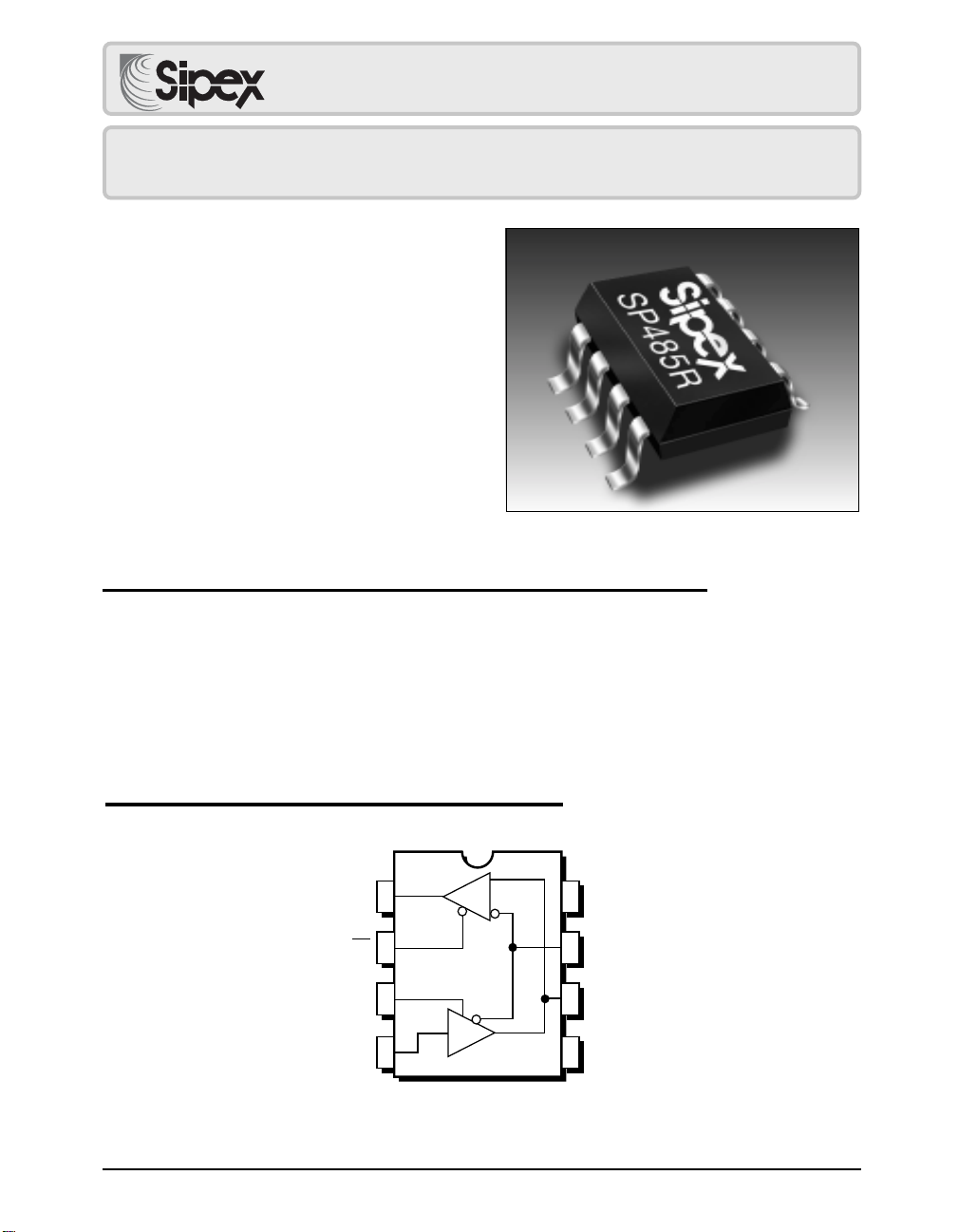
SP481R/SP485R
Now Available in Lead Free Packaging
DESCRIPTION
The SP481R and SP485R are pin-to-pin equivalent with our existing SP485 product and contain
enhancements such as higher ESD tolerance and high receiver input impedance. The higher
receiver input impedance allows for connecting over 400 transceivers on a single transmission
line without degrading the RS-485 driver signal. Each device is packaged in an 8-pin plastic DIP
or 8-pin narrow SOIC package. The SP481R offers a shutdown feature via the enable pins which
will reduce the supply current (ICC) below 0.5µA typical.
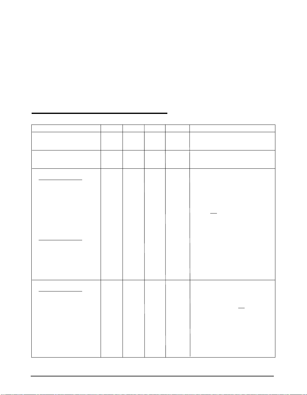
TYPICAL APPLICATION CIRCUIT
RO 1
RE 2
DE 3
R
8 V
7 B
6 A
CC
D
DI 4
SP485
Top View
5 GND
Date: 6/21/04 SP485R RS-485 Serial Transceiver © Copyright 2004 Sipex Corporation
1
Page 2
ABSOLUTE MAXIMUM RATINGS
These are stress ratings only and functional operation
of the device at these ratings or any other above those
indicated in the operation sections of the specifications
below is not implied. Exposure to absolute maximum
rating conditions for extended periods of time may
affect reliability.
...........................................................................+7V
V
CC
Storage Temperature..........................-65˚C to +150˚C
Power Dissipation
8-pin Plastic DIP...........................1000mW
8-pin Plastic N-SOIC.......................1000mW
Package Derating:
8-pin Plastic DIP
ø
....................................................62 °C/W
8-pin Plastic N-SOIC
JA
øJA....................................................62 °C/W
ELECTRICAL CHARACTERISTICS
Typically 25°C @ Vcc = +5V unless otherwise noted.
MIN. TYP. MAX. UNITS CONDITIONS
LOGIC INPUTS
V
IL
V
IH
2.0 Volts
LOGIC OUTPUTS
V
OL
V
OH
2.4 Volts I
RS-485 DRIVER
DC Characteristics
TTL Input Levels
V
IL
V
IH
Outputs
2.0 Volts
Open Circuit Voltage 6.0 Volts
Differential Output 1.5 5.0 Volts RL=54Ω, CL=50pF
Balance ±0.2 Volts |VT| - |VT|
Common-Mode Output 3.0 Volts
Output Current 28.0 mA RL=54Ω
Short Circuit Current ±250 mA Terminated in –7V to +12V
AC Characteristics
Maximum Data Rate 5 Mbps RL=54Ω
Output Transition Time 30 ns Rise/fall time, 10%–90%
Propagation Delay See Figures 3 and 5
t
PHL
t
PLH
Driver Output Skew 5 15 ns see Figure 3 and 5,
60 100 ns R
60 100 ns R
RS-485 RECEIVER
DC Characteristics
TTL Output Levels
V
OL
V
OH
Tri-State Output Current ±1 µA 0.4V≤V
2.4 Volts
Inputs
Common Mode Range –7.0 +12.0 Volts
Receiver Sensitivity ±0.2 Volts –7V ≤ V
Input Impedance 120 150 kΩ –7V ≤ V
0.8 Volts
0.4 Volts I
0.8 Volts
0.4 Volts
= -3.2mA
OUT
= 1.0mA
OUT
=54Ω, CL1=CL2=100pF
DIFF
=54Ω, CL1=CL2=100pF
DIFF
t
SKEW
= | t
- t
DPLH
≤2.4V; RE = V
OUT
≤ +12V
CM
≤ +12V
CM
DPHL
|
CC
Date: 6/21/04 SP485R RS-485 Serial Transceiver © Copyright 2004 Sipex Corporation
2
Page 3
ELECTRICAL CHARACTERISTICS
Typically 25°C @ Vcc = +5V unless otherwise noted.
MIN. TYP. MAX. UNITS CONDITIONS
AC Characteristics
Maximum Data Rate 1 Mbps
Propagation Delay See Figures 3 and 7
t
PHL
t
PLH
Differential Receiver Skew 60 ns | t
SHUTDOWN TIMING (SP481R)
Time to Shutdown 50 600 ns RE = VCC, DE = 0V
RS-485 Driver
Enable Time See Figures 4 and 6
Enable to Low 40 500 ns CL=15pF, S1 Closed
Enable to High 40 500 ns CL=15pF, S2 Closed
Disable Time See Figures 4 and 6
Disable From Low 40 500 ns CL=15pF, S1 Closed
Disable From High 40 500 ns CL=15pF, S2 Closed
RS-485 Receiver
Enable Time See Figures 2 and 8
Enable to Low 40 500 ns CL=15pF, S1 Closed
Enable to High 40 500 ns CL=15pF, S2 Closed
Disable Time See Figures 2 and 8
Disable From Low 40 500 ns CL=15pF, S1 Closed
Disable From High 40 500 ns CL=15pF, S2 Closed
POWER REQUIREMENTS
Supply Voltage V
Supply Current I
No Load 300 500 µA RE = VCC or 0V, DE = 0V
CC
CC
+4.75 +5.25 Volts
No Load 500 900 µA RE = VCC or 0V, DE = V
Supply Current in Shutdown 0.5 10 µA RE = VCC, DE = OV
1200 ns R
1200 ns R
=54Ω, CL1=CL2=100pF
DIFF
=54Ω, CL1=CL2=100pF
DIFF
– t
PHL
|; R
PLH
CL1=CL2=100pF, see Figures 3 and 7
DIFF
=54Ω,
CC
ENVIRONMENTAL
Operating Temperature
Commercial (..C..) 0 +70 °C
Industrial (..E..) –40 +85 °C
Storage Temperature –65 +150 °C
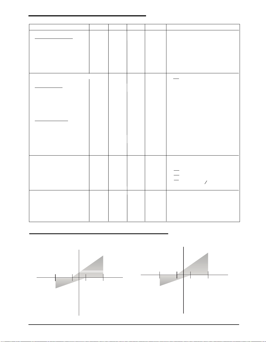
RECEIVER INPUT GRAPH
-7V
-60µA
SP485R Reciever
-3V
+6V
1/10 Unit Load
Maximum Input Current
versus voltage.
(Shaded region)
+100µA
+12V
Standard SP485R Reciever
+1.0mA
-7V
-0.6 mA
Date: 6/21/04 SP485R RS-485 Serial Transceiver © Copyright 2004 Sipex Corporation
-3V
+6V
1 Unit Load
Maximum Input Current
versus voltage.
(Shaded region)
+12V
3
Page 4

TEST CIRCUITS
+3V
0V
DI
DRIVER
OUTPUT
DIFFERENTIAL
OUTPUT
– V
0V
1.5V
1.5V
PLH
f = 1MHz; t
< 10ns; t
< 10ns
1/2V
1/2V
PHL
SKEW
= |
DPLH
DPHL
DPLH
DPHL
PLH
A
R
V
OD
V
OC
R
B
Figure 1. Driver DC Test Load Circuit
C
DI
A
B
L1
R
L
C
L2
Figure 3. Driver/Receiver Timing Test Circuit
A
B
RO
15pF
Receiver
Output
Test Point
RL
1kΩC
1kΩ
S
1
S
2
Figure 2. Receiver Timing Test Load Circuit
S
Output
500Ω
1
Under
Test
C
L
S
2
Figure 4. Driver Timing Test Load #2 Circuit
V
CC
V
CC
SWITCHING WAVEFORMS
Figure 5. Driver Propagation Delays
Date: 6/21/04 SP485R RS-485 Serial Transceiver © Copyright 2004 Sipex Corporation
DRIVER
OUTPUT
DIFFERENTIAL
OUTPUT
VA – V
t
= |
t
DPLH
SKEW
DI
B
- t
+3V
V
V
DPHL
0V
O
0V
O
B
A
+
–
V
O
|
1/2V
f = 1MHz; t
1.5V
O
4
< 10ns; t
R
t
PLH
t
DPLH
t
R
F
t
< 10ns
t
PHL
DPHL
1.5V
t
PLH
1/2V
t
F
O
Page 5

+3V
DE
1.5V 1.5V
0V
5V
A, B
V
OL
V
OH
A, B
0V
Figure 6. Driver Enable and Disable Times
+
V
0D2
A – B
RECEIVER OUT
–
V
0D2
V
OH
V
OL
t
PHL
f = 1MHz; tR < 10ns; tF < 10ns
t
ZL
2.3V
2.3V
Output normally LOW
Output normally HIGH
t
ZH
f = 1MHz; tR < 10ns; tF < 10ns
0V 0V
1.5V 1.5V
INPUT
OUTPUT
t
PLH
0.5V
0.5V
t
LZ
t
HZ
t
= | t
- t
SKEW
Figure 7. Receiver Propagation Delays
PHL
PLH
|
+3V
RE
0V
1.5V 1.5V
f = 1MHz; tR < 10ns; tF < 10ns
t
ZL
t
LZ
5V
RECEIVER OUT
V
IL
V
IH
RECEIVER OUT
0V
Figure 8. Receiver Enable and Disable Times
Date: 6/21/04 SP485R RS-485 Serial Transceiver © Copyright 2004 Sipex Corporation
1.5V
1.5V
Output normally LOW
Output normally HIGH
t
ZH
0.5V
0.5V
t
HZ
5
Page 6

GENERAL DESCRIPTION
The SP485R is a low power RS-485 differential
transceiver. Similar to the SP485, the SP485R
contains a half-duplex driver and receiver with
tri-state control. However, the SP485R is intended for increased connections on a single bus
compared to the orignal RS-485 specification.
The RS-485 standard is ideal for multi-drop
applications where one bus can contain many
drivers and/or receivers. The RS-485 standard
implementation allows up to 32 transceivers to
be connected on to the data bus. RS-485 is also
specified for driving higher speeds over long
cable lengths of up to 4,000 feet. The SP485R
and SP481R exceed the standard b allowing up
to 400 receivers to share a bus.
DRIVERS
The driver output complies with the RS-485
electrical characteristics as specified by the
standard. The output swings from 0V to VCC and
maintains greater than +1.5V with a 54Ω load
attached between the two outputs. In adhering
to the RS-485 specification, the driver outputs
inherently comply with the RS-422 standard.
With a load of 100Ω between the two outputs,
the driver can sustain at least +2.0V.
with the two 125Ω cable termination resistors
on each end.
The receiver contains a enable pin (RE) which
enables the receiver when a logic LOW is
asserted. A logic HIGH will tri-state the
receiver output and the inputs will maintain
at least 120kΩ impedance. The receiver can
operate to at least 1Mbps.
The receiver also contains a fail-safe feature
which outputs a logic HIGH when the inputs are
open as in a disconnected cable.
SHUTDOWN MODE
The SP481R includes a shutdown function to
reduce power consumption. The shutdown is
activated by simultaneously applying a logic
LOW to DE and a logic HIGH to RE. While in
the shutdown mode, the power supply current is
typically less than 1µA. The driver outputs are
disabled and are at a high impedance state
determined by the receiver input impedance
which should be at least 120kΩ. The receiver
output is at also at high impedance during
shutdow. Output leakage current when the
receiver is disabled is under 1µA.
The driver contains an enable pin (DE) which
tri-states the output when DE is a logic LOW.
The outputs
during the tri-stated condition are
at a high impedance (>100kΩ). A logic HIGH
enables the driver for normal operation. The
driver can operate to at least 5Mbps
.
RECEIVERS
The SP485R receiver has differential inputs
with an input sensitivity of lower than ±200mV.
As mentioned above, the RS-485 specification
allows up to 32 transceivers on a the same bus.
The SP485R allows over 400 transceivers on
the same bus due to the high input impedance of
at least 120kΩ. This higher capacity allows
more components to be attached to the same
bus without degrading the signal quality. The
drivers are still able to drive an equivalent 54Ω
from the 320 transceivers with an input
impedance of at least 120kΩ in parallel along
Date: 6/21/04 SP485R RS-485 Serial Transceiver © Copyright 2004 Sipex Corporation
6
Page 7

PACKAGE: 8 PIN PDIP
INDEX
AREA
D1
N
1
b3
8 PIN PDIP
JEDEC MS-001
(BA) V ariation
23
D
e
A
A1
A2
b
b2
b3
c
D
D1
E
E1
e
eA
eB
L
.115 .130 .150
N/2
b2
b
Dimensions in inches
MIN NOM MAX
- - .210
.015 .115 .130 .195
.014 .018 .022
.045 .060 .070
.030 .039 .045
.010 .014
.008
.355
.365
--
.005
.310
.300
.240 .250 .280
.100 BSC
.300 BSC
-
-
.400
.325
.430
E1
L
-
A1
E
E
c
eA
eB
A
A2
b
c
8 PIN PDIP
Date: 6/21/04 SP485R RS-485 Serial Transceiver © Copyright 2004 Sipex Corporation
7
Page 8

PACKAGE: 8 PIN NSOIC
D
e
E/2
E1
E
INDEX AREA
(D/2 X E1/2)
1
TOP VIEW
A
Minimum/Maximum
A2
A1
DIMENSIONS
(mm)
COMMON HEIGHT DIMENSION
SYMBOL MIN NOM MAX
A
A1
A2
b
c
1.35
0.10
1.25
0.31
0.17 0.25
D
E
E1
e
L
0.40
L1
L2
Ø
Ø1
0º
5º
A
SIDE VIEW
8 Pin NSOIC
(JEDEC MS-012,
AA - VARIATION)
1.75
-
- 0.25
-
1.65
-
0.51
-
4.90 BSC
6.00 BSC
3.90 BSC
1.27 BSC
-
1.27
1.04 REF
0.25 BSC
-
8º
-
15º
E1/2
b
Ø1
Seating Plane
Ø1
SEE VIEW C
L
L1
L2
Gauge Plane
Ø
VIEW C
SEATING PLANE
WITH PLATING
b
c
BASE METAL
CONT ACT AREA
PACKAGE:
8 PIN NSOIC
Date: 6/21/04 SP485R RS-485 Serial Transceiver © Copyright 2004 Sipex Corporation
8
Page 9

ORDERING INFORMATION
Part Number Temperature Range Package Types
SP481RCP ........................................................................0°C to +70°C ................................................................................................ 8 Pin PDIP
SP481RCN........................................................................ 0°C to +70°C ............................................................................................. 8 Pin NSOIC
SP481RCN/TR.................................................................. 0°C to +70°C ............................................................................................. 8 Pin NSOIC
SP481REP .....................................................................-40°C to +85°C ................................................................................................ 8 Pin PDIP
SP481REN .....................................................................-40° C to +85°C ............................................................................................. 8 Pin NSOIC
SP481REN/TR ...............................................................-40° C to +85°C ............................................................................................. 8 Pin NSOIC
SP485RCP ........................................................................0°C to +70°C ................................................................................................ 8 Pin PDIP
SP485RCN........................................................................ 0°C to +70°C ................................................................................................ 8 Pin NOIC
SP485RCN/TR.................................................................. 0°C to +70°C ................................................................................................ 8 Pin NOIC
SP485REP .....................................................................-40°C to +85°C ................................................................................................ 8 Pin PDIP
SP485REN .....................................................................-40° C to +85°C ................................................................................................ 8 Pin NOIC
SP485REN/TR ...............................................................-40° C to +85°C ................................................................................................ 8 Pin NOIC
Available in lead free packaging. To order add “-L” suffix to part number.
Example: SP485REN/TR = standard; SP485REN-L/TR = lead free
/TR = Tape and Reel
Pack quantity is 2,500 for NSOIC.
REVISION HISTORY
DATE REVISION DESCRIPTION
6/21/04 A Added extended temp range and tape and reel part numbers. Updated
packaging specs.
Corporation
ANALOG EXCELLENCE
Sipex Corporation
Headquarters and
Sales Office
233 South Hillview Drive
Milpitas, CA 95035
TEL: (408) 934-7500
FAX: (408) 935-7600
Sipex Corporation reserves the right to make changes to any products described herein. Sipex does not assume any liability arising out of the
application or use of any product or circuit described herein; neither does it convey any license under its patent rights nor the rights of others.
Date: 6/21/04 SP485R RS-485 Serial Transceiver © Copyright 2004 Sipex Corporation
9
 Loading...