

Page 1

THIS DOCUMENT IS FOR MAINTENANCE
PURPOSES ONLY AND IS NOT
RECOMMENDED FOR NEW DESIGNS
Page 2
SP4740
1·3GHz 44256 PRESCALER WITH LOW CURRENT AND LOW RADIATION
The SP4740 4256 prescaler is one of GPS’ range of high
speed dividers for consumer frequency synthesis and
measurement systems. It has a low supply current, giving reduced
dissipation and operating temperatures in an 8-pin plastic DIL
(DP8) or miniature plastic DIL (MP8) package. Spurious radiation
has been reduced from all stages.
The SP4740 incorporates an on-chip preamplifier with
differential inputs and has a TTL/CMOS compatible output.
FEATURES
■ Low Supply Current
■ Low Radiation
■
Input Wideband Amplifier
■ High Input Sensitivity
■ High Input Impedance
■ TTL/CMOS Output
■ Electrostatic Protection †
† ESD precautions must be observed
1
INPUT
2
SP4740
3
V
CC
4
V
CC
1
INPUT
2
V
CC
V
CC
3
4
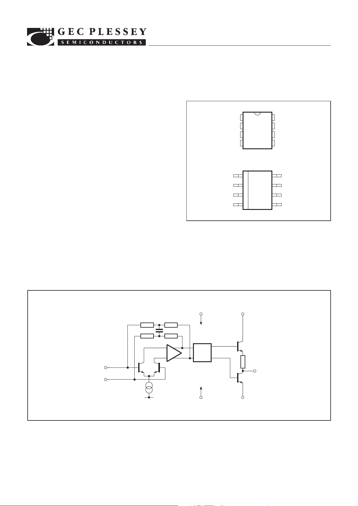
Fig 1. Pin connections - top view
SP4740
8
7
6
5
8
7
6
5
0V
0V
OUTPUT
0V
0V
OUTPUT
3062-2.2
DP8
MP8
ABSOLUTE MAXIMUM RATINGS
Supply voltage, V
Input voltage
Storage temperature
Operating temperature range
CC
DIFFERENTIAL
INPUT
1
2
17V
2·5V p-p
255°C to 1150°C
0°C to180°C
1k
1k
2k
2k
Fig. 2 SP4740 block diagram
ORDERING IFORMATION
SP4740 NA DP
SP4740 NA MP
V
CC
4256
0V
3
8
V
CC
4
600
5
7
0V
OUTPUT
Page 3

SP4740
ELECTRICAL CHARACTERISTICS
These characteristics are guaranteed over the following conditions (unless otherwise stated):
T
= 0°C to 170°C, V
AMB
Characteristic
= 4·5V to 5·5V (Test circuit see Fig. 3)
CC
Pin
Min.
Value
Typ. Max.
Units
Conditions
Supply current, I
Input sensitivity
50MHz
150MHz to 1000MHz
1·1GHz
1·2GHz
1·3GHz
Input overload
Input impedance
CC
8
2,3
2,3
2,3
300
400
35
3
1
1·5
2
4
50
2
50
mA
V
= 15V
CC
RMS sinewave
5
mV
5
mV
mV
mV
mV
mV
mV
50MHz to 500MHz
500MHz to 1·3GHz
Ω
See Fig. 6
pF
Output voltage
3·3
High
Low
5
5
0·1
NOTE
The difference between the maximum input sensitivity and minimum overload voltage is the guaranteed dynamic range. Input signal levels should
be maintained within these limits at all frequencies.
50 Ω
SAMPLING
SCOPE
180°
HYBRID
COUPLER
0V
D
15V
V
V
Sourcing 0·2mA
Sinking 2mA
115V
50 Ω
SIGNAL
GENERATOR
FROM
50Ω
SOURCE
A
UHF INPUT
VHF INPUT
B
50
1n
1n
1 TURN
100p
1n
C
0·1µ
1n
Fig. 3 Test circuit
15V
1
2
3
4
12p
0·1µ
Fig. 4 Application circuit
1
2
SP4740
3
4
SP4740
8
7
6
5
8
7
CMOS OR
TTL GATE
6
5
6·5k
OUTPUT
1·65k
0V
0V
2
Page 4

26
24
22
20
18
16
14
12
10
(mV RMS INTO 50Ω )
IN
8
V
6
4
2
0
0 200 400 600 800 1000 1200 1400 1600
SPECIFICATION LIMIT
TYPICAL DEVICE
FREQUENCY (MHz)
SP4740
Fig. 5 Typical input sensitivity
j
1
j
0.5
j
0.2
0.5
j
0.5
1300
1
j
2
2
1000
800
1
S
11
Z
O
0
2
= 50Ω
0.2
j
0.2
2
Fig. 6 Typical input impedance (frequencies in MHz)
600
j
2
60
5
j
2
j
5
200
j
5
2
400
2
3
Page 5

SP4740
HEADQUARTERS OPERATIONS
GEC PLESSEY SEMICONDUCTORS
Cheney Manor, Swindon,
Wiltshire SN2 2QW, United Kingdom.
Tel: (0793) 518000
Fax: (0793) 518411
GEC PLESSEY SEMICONDUCTORS
P.O. Box 660017
1500 Green Hills Road,
Scotts Valley, California 95067-0017,
United States of America.
Tel: (408) 438 2900
Fax: (408) 438 5576
CUSTOMER SERVICE CENTRES
• FRANCE & BENELUX Les Ulis Cedex Tel: (1) 64 46 23 45 Tx: 602858F
Fax : (1) 64 46 06 07
• GERMANY Munich Tel: (089) 3609 06-0 Tx: 523980 Fax : (089) 3609 06-55
• ITALY Milan Tel: (02) 66040867 Fax: (02) 66040993
• JAPAN Tokyo Tel: (03) 3296-0281 Fax: (03) 3296-0228
• NORTH AMERICA Integrated Circuits and Microwave Products Scotts Valley, USA
Tel (408) 438 2900 Fax: (408) 438 7023.
Hybrid Products, Farmingdale, USA Tel (516) 293 8686
Fax: (516) 293 0061.
• SOUTH EAST ASIA Singapore Tel: (65) 3827708 Fax: (65) 3828872
• SWEDEN Stockholm, Tel: 46 8 702 97 70 Fax: 46 8 640 47 36
• UNITED KINGDOM & SCANDINAVIA
Swindon Tel: (0793) 518510 Tx: 444410 Fax : (0793) 518582
These are supported by Agents and Distributors in major countries world-wide.
GEC Plessey Semiconductors 1996 Publication No. DS3062 Issue No. 2.2 May 1996
This publication is issued to provide information only which (unless agreed by the Company in writing) may not be used, applied or reproduced for any purpose nor form part of any order or contract nor to be regarded
4
as a representation relating to the products or services concerned. No warranty or guarantee express or implied is made regarding the capability, performance or suitability of any product or service. The Company
reserves the right to alter without prior knowledge the specification, design or price of any product or service. Information concerning possible methods of use is provided as a guide only and does not constitute
any guarantee that such methods of use will be satisfactory in a specific piece of equipment. It is the user's responsibility to fully determine the performance and suitability of any equipment using such information
and to ensure that any publication or data used is up to date and has not been superseded. These products are not suitable for use in any medical products whose failure to perform may result in significant injury
or death to the user. All products and materials are sold and services provided subject to the Company's conditions of sale, which are available on request.
Page 6

For more information about all Zarlink products
visit our Web Site at
www.zarlink.com
Information relating to products and services furnished herein by Zarlink Semiconductor Inc. trading as Zarlink Semiconductor or its subsidiaries (collectively
“Zarlink”) is believed to be reliable. However, Zarlink assumes no liability for errors that may appear in this publication, or for liability otherwise arising from the
application or use of any such information, product or service or for any infringement of patents or other intellectual property rights owned by third parties which may
result from such application or use. Neither the supply of such information or purchase of product or service conveys any license, either express or implied, under
patents or other intellectual property rights owned by Zarlink or licensed from third parties by Zarlink, whatsoever. Purchasers of products are also hereby notified
that the use of product in certain ways or in combination with Zarlink, or non-Zarlink furnished goods or services may infringe patents or other intellectual property
rights owned by Zarlink.
This publication is issued to provide information only and (unless agreed by Zarlink in writing) may not be used, applied or reproduced for any purpose nor form part
of any order or contract nor to be regarded as a representation relating to the products or services concerned. The products, their specifications, services and other
information appearing in this publication are subject to change by Zarlink without notice. No warranty or guarantee express or implied is made regarding the
capability, performance or suitability of any product or service. Information concerning possible methods of use is provided as a guide only and does not constitute
any guarantee that such methods of use will be satisfactory in a specific piece of equipment. It is the user ’s responsibility to fully determine the performance and
suitability of any equipment using such information and to ensure that any publication or data used is up to date and has not been superseded. Manufacturing does
not necessarily include testing of all functions or parameters. These products are not suitable for use in any medical products whose failure to perform may result in
significant injury or death to the user. All products and materials are sold and services provided subject to Zarlink’s conditions of sale which are available on request.
Purchase of Zarlink’s I
conforms to the I
Zarlink and the Zarlink Semiconductor logo are trademarks of Zarlink Semiconductor Inc.
Copyright 2002, Zarlink Semiconductor Inc. All Rights Reserved.
2
C components conveys a licence under the Philips I2C Patent rights to use these components in an I2C System, provided that the system
2
C Standard Specification as defined by Philips.
TECHNICAL DOCUMENTATION - NOT FOR RESALE
 Loading...