

Page 1
SL74HC4015
Semiconductor
Dual 4-Bit Shift Register
High-Performance Silicon-Gate CMOS
The device inputs are compatible with standard CMOS outputs;
with pullup resistors, they are compatible with LS/ALSTTL outputs.
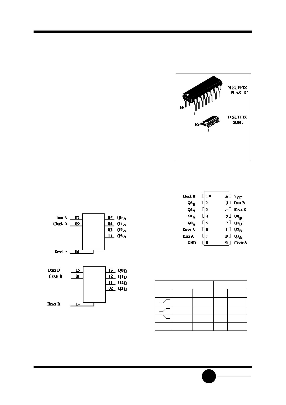
This device consists of two identical independent 4-stage serialinput/parallel-output registers. Each register has independent Clock
and Reset inputs as well as a single serial Data input. “Q” outputs are
available from each of the four stages on both registers. All register
stages are D-type, master -slave flip-flops. The logic level present at the
Data input is transferred into the first register stage and shifted over
one stage at each positive-going clock transition. Resetting of all
stages is accomplished by a high level on the reset line.
• Outputs Directly Interface to CMOS, NMOS, and TTL
• Operating Voltage Range: 2.0 to 6.0 V
• Low Input Current: 1.0 µA
• High Noise Immunity Characteristic of CMOS Devices
ORDERING INFORMATION
SL74HC4015N Plastic
SL74HC4015D SOIC
TA = -55° to 125° C for all packages
LOGIC DIAGRAM
PIN 16 = VCC
PIN 8 = GND
PIN ASSIGNMENT
FUNCTION TABLE
Inputs Outputs
Clock Data Reset Q0 Qn
L L L Q
H L H Q
X L Q
X X H L L
*
= No Change
X = don’t care
*
0
Q
n-1
n-1
*
n
System Logic
SLS
Page 2
SL74HC4015
Semiconductor
MAXIMUM RATINGS*
Symbol Parameter Value Unit
VCC DC Supply Voltage (Referenced to GND) -0.5 to +7.0 V
VIN DC Input Voltage (Referenced to GND) -1.5 to VCC +1.5 V
V
DC Output Voltage (Referenced to GND) -0.5 to VCC +0.5 V
OUT
IIN DC Input Current, per Pin ±20 mA
I
DC Output Current, per Pin ±25 mA
OUT
ICC DC Supply Current, VCC and GND Pins ±50 mA
PD Power Dissipation in Still Air, Plastic DIP+
SOIC Package+
750
500
Tstg Storage Temperature -65 to +150 °C
TL Lead Temperature, 1 mm from Case for 10 Seconds
260 °C
(Plastic DIP or SOIC Package)
*
Maximum Ratings are those values beyond which damage to the device may occur.
Functional operation should be restricted to the Recommended Operating Conditions.
+Derating - Plastic DIP: - 10 mW/°C from 65° to 125°C
SOIC Package: : - 7 mW/°C from 65° to 125°C
RECOMMENDED OPERATING CONDITIONS
Symbol Parameter Min Max Unit
VCC DC Supply Voltage (Referenced to GND) 2.0 6.0 V
VIN, V
DC Input Voltage, Output Voltage (Referenced to GND) 0 VCC V
OUT
TA Operating Temperature, All Package Types -55 +125 °C
tr, tf Input Rise and Fall Time (Figure 1) VCC =2.0 V
VCC =4.5 V
V
=6.0 V
CC
0
0
0
1000
500
400
mW
ns
This device contains protection circuitry to guard against damage due to high static voltages or electric
fields. However, precautions must be taken to avoid applications of any voltage higher than maximum rated
voltages to this high-impedance circuit. For proper operation, VIN and V
GND≤(VIN or V
OUT
)≤VCC.
should be constrained to the range
OUT
Unused inputs must always be tied to an appropriate logic voltage level (e.g., either GND or VCC).
Unused outputs must be left open.
System Logic
SLS
Page 3

SL74HC4015
Semiconductor
DC ELECTRICAL CHARACTERISTICS(Voltages Referenced to GND)
VCC Guaranteed Limit
Symbol Parameter Test Conditions V 25 °C
to
-55°C
VIH Minimum High-Level
Input Voltage
VIL Maximum Low -Level
Input Voltage
VOH Minimum High-Level
Output Voltage
VIN= VIH or VIL
VOL Maximum Low -Level
Output Voltage
VIN= VIH or VIL
IIN Maximum Input
V
= 0.1 V or VCC-0.1 V
OUT
I
≤ 20 µA
OUT
V
=0.1 V or VCC-0.1 V
OUT
I
≤ 20 µA
OUT
VIN=VIH or VIL
I
≤ 20 µA
OUT
I
≤ 4.0 mA
OUT
I
≤ 5.2 mA
OUT
VIN=VIH or VIL
I
≤ 20 µA
OUT
I
≤ 4.0 mA
OUT
I
≤ 5.2 mA
OUT
2.0
4.5
6.0
2.0
4.5
6.0
2.0
4.5
6.0
4.5
6.0
2.0
4.5
6.0
4.5
6.0
1.5
3.15
4.2
0.3
0.9
1.2
1.9
4.4
5.9
3.98
5.48
0.1
0.1
0.1
0.26
0.26
VIN=VCC or GND 6.0 ±0.1 ±1.0 ±1.0 µA
Leakage Current
≤85
°C
1.5
3.15
4.2
0.3
0.9
1.2
1.9
4.4
5.9
3.84
5.34
0.1
0.1
0.1
0.33
0.33
≤125
°C
1.5
3.15
4.2
0.3
0.9
1.2
1.9
4.4
5.9
3.7
5.2
0.1
0.1
0.1
0.4
0.4
Unit
V
V
V
V
ICC Maximum Quiescent
Supply Current
(per Package)
VIN=VCC or GND
I
=0µA
OUT
6.0 8.0 80 160 µA
System Logic
SLS
Page 4

SL74HC4015
Semiconductor
AC ELECTRICAL CHARACTERISTICS(C
VCC Guaranteed Limit
=50pF,Input tr=tf=6.0 ns)
L
Symbol Parameter V 25 °C to
≤85°C ≤125°C Unit
-55°C
f
Maximum Clock Frequency (50% Duty Cycle)
max
(Figure 2)
t
, t
PLH
Maximum Propagation Delay, Clock to Q (Figures
PHL
2 and 5)
t
Maximum Propagation Delay, Reset to Q (Figures
PHL
1 and 5)
t
, t
TLH
Maximum Output Transition Time, Any Output
THL
(Figures 3 and 5)
2.0
4.5
6.0
2.0
4.5
6.0
2.0
4.5
6.0
2.0
4.5
6.0
6
30
35
175
35
30
205
41
35
75
15
13
4.8
24
28
220
44
37
255
51
43
95
19
16
4
20
24
265
53
45
310
62
53
110
22
19
CIN Maximum Input Capacitance - 10 10 10 pF
Power Dissipation Capacitance (Per Latch) Typical @25°C,VCC=5.0 V
CPD Used to determine the no-load dynamic power
consumption: PD=CPDV
TIMING REQUIREMENTS(C
2
f+ICCVCC
CC
=50pF,Input tr=tf=6.0 ns)
L
140 pF
MHz
ns
ns
ns
VCC Guaranteed Limit
Symbol Parameter V 25 °C to
≤85°C ≤125°C Unit
-55°C
tsu Minimum Setup Time, D to Clock
(Figure 4)
th Minimum Hold Time, Clock to D
(Figure 4)
t
Minimum Recovery Time, Reset to
rec
Clock (Figure 1)
tw Minimum Pulse Width, Reset (Figure
1)
tw Minimum Pulse Width, Clock (Figure
4)
tr, tf Maximum Input Rise and Fall Times
(Figure 1)
2.0
4.5
6.0
2.0
4.5
6.0
2.0
4.5
6.0
2.0
4.5
6.0
2.0
4.5
6.0
2.0
4.5
6.0
50
10
9.0
5
5
5
5
5
5
80
16
14
80
16
14
1000
500
400
65
13
11
5
5
5
5
5
5
100
20
17
100
20
17
1000
500
400
75
15
13
5
5
5
5
5
5
120
24
20
120
24
20
1000
500
400
ns
ns
ns
ns
ns
ns
SLS
System Logic
Page 5

SL74HC4015
Semiconductor
Figure 1. Switching Waveforms Figure 2. Switching Waveforms
Figure 3. Switching Waveforms Figure 4. Switching Waveforms
Figure 5. Test Circuit
SLS
System Logic
Page 6

SL74HC4015
Semiconductor
EXPANDED LOGIC DIAGRAM
SLS
System Logic
Page 7

WWW.ALLDATASHEET.COM
Copyright © Each Manufacturing Company.
All Datasheets cannot be modified without permission.
This datasheet has been download from :
www.AllDataSheet.com
100% Free DataSheet Search Site.
Free Download.
No Register.
Fast Search System.
www.AllDataSheet.com
 Loading...