

Page 1
SL74HC652
Semiconductor
Octal 3-State Bus Transceivers and D Flip-Flops
High-Performance Silicon-Gate CMOS
The SL74HC652 is identical in pinout to the LS/ALS652. The device
inputs are compatible with standard CMOS outputs; with pullup
resistors, they are compatible with LS/ALSTTL outputs.
These devices consists of bus transceiver circuits, D-type flip -flop,
and control circuitry arranged for multiplex transmission of data
directly from the data bus or from the internal storage registers.
Direction and Output Enable are provided to select the read-time or
stored data function. Data on the A or B Data bus, or both, can be
stored in the internal D flip-flops by low-to-high transitions at the
appropriate clock pins (A-to-B Clock or B-to-A Clock) regardless of the
select or enable or enable control pins. When A-to-B Source and B-toA Source are in the real-time transfer mode, it is also possible to store
data without using the internal D-type flip -flops by simulta-neously
enabling Direction and Output Enable. In this configuration each
output reinforces its input. Thus, when all other data sources to the
two sets of bus lines are at high impedance, each set of bus lines will
remain at its last state.
The SL74HC652 has noninverted outputs.
• Outputs Directly Interface to CMOS, NMOS, and TTL
• Operating Voltage Range: 2.0 to 6.0 V
• Low Input Current: 1.0 µA
• High Noise Immunity Characteristic of CMOS Devices
ORDERING INFORMATION
SL74HC652N Plastic
SL74HC652D SOIC
TA = -55° to 125° C for all packages
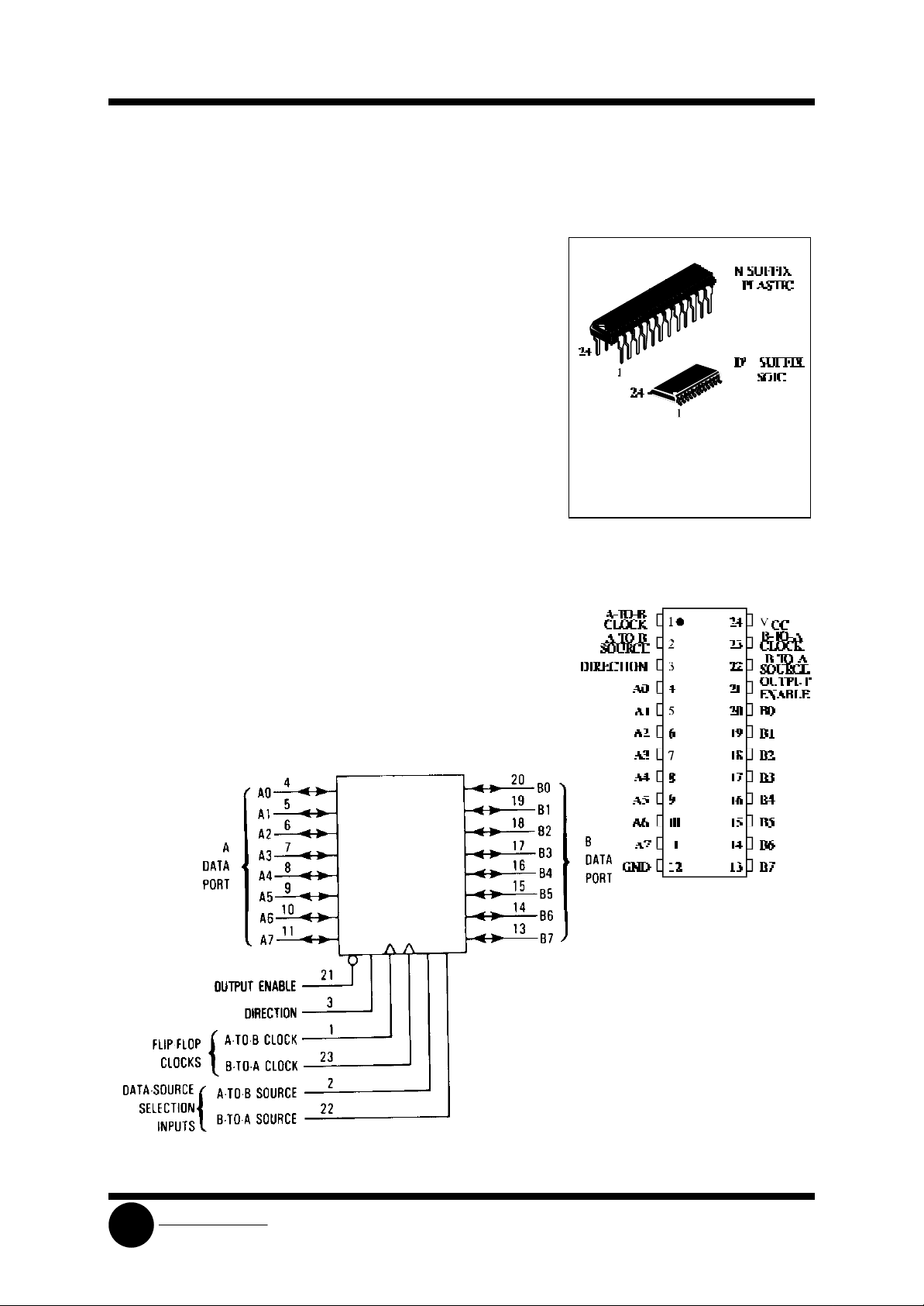
PIN ASSIGNMENT
LOGIC DIAGRAM
PIN 24=VCC
PIN 12 = GND
SLS
System Logic
Page 2
SL74HC652
Semiconductor
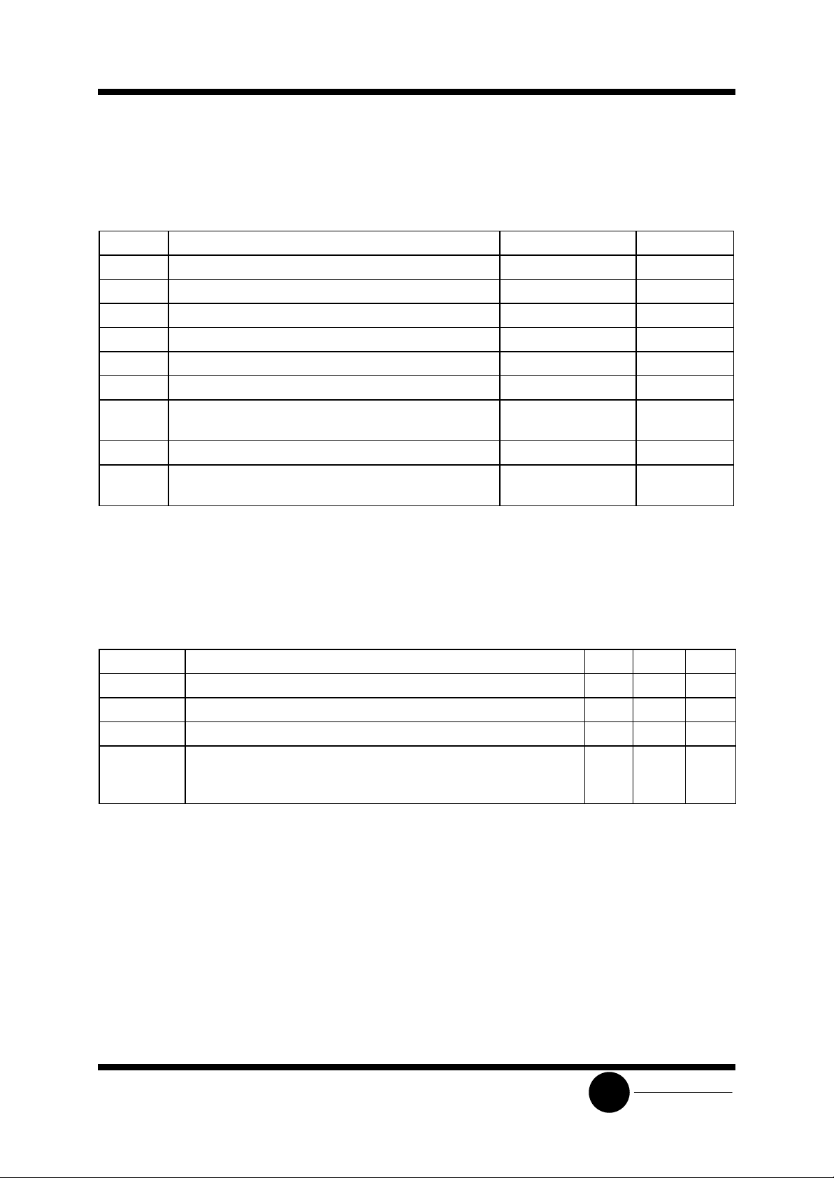
MAXIMUM RATINGS*
Symbol Parameter Value Unit
VCC DC Supply Voltage (Referenced to GND) -0.5 to +7.0 V
VIN DC Input Voltage (Referenced to GND) -1.5 to VCC +1.5 V
V
DC Output Voltage (Referenced to GND) -0.5 to VCC +0.5 V
OUT
IIN DC Input Current, per Pin ±20 mA
I
DC Output Current, per Pin ±35 mA
OUT
ICC DC Supply Current, VCC and GND Pins ±75 mA
PD Power Dissipation in Still Air, Plastic DIP+
SOIC Package+
750
500
Tstg Storage Temperature -65 to +150 °C
TL Lead Temperature, 1 mm from Case for 10 Seconds
260 °C
(Plastic DIP or SOIC Package)
*
Maximum Ratings are those values beyond which damage to the device may occur.
Functional operation should be restricted to the Recommended Operating Conditions.
+Derating - Plastic DIP: - 10 mW/°C from 65° to 125°C
SOIC Package: : - 7 mW/°C from 65° to 125°C
RECOMMENDED OPERATING CONDITIONS
Symbol Parameter Min Max Unit
VCC DC Supply Voltage (Referenced to GND) 2.0 6.0 V
VIN, V
DC Input Voltage, Output Voltage (Referenced to GND) 0 VCC V
OUT
TA Operating Temperature, All Package Types -55 +125 °C
tr, tf Input Rise and Fall Time (Figures2,3) VCC =2.0 V
VCC =4.5 V
V
=6.0 V
CC
0
1000
0
0
500
400
mW
ns
This device contains protection circuitry to guard against damage due to high static voltages or electric
fields. However, precautions must be taken to avoid applications of any voltage higher than maximum rated
voltages to this high-impedance circuit. For proper operation, VIN and V
GND≤(VIN or V
OUT
)≤VCC.
should be constrained to the range
OUT
Unused inputs must always be tied to an appropriate logic voltage level (e.g., either GND or VCC).
Unused outputs must be left open. I/O pins must be connected to a properly ter minated line or bus.
System Logic
SLS
Page 3
SL74HC652
Semiconductor
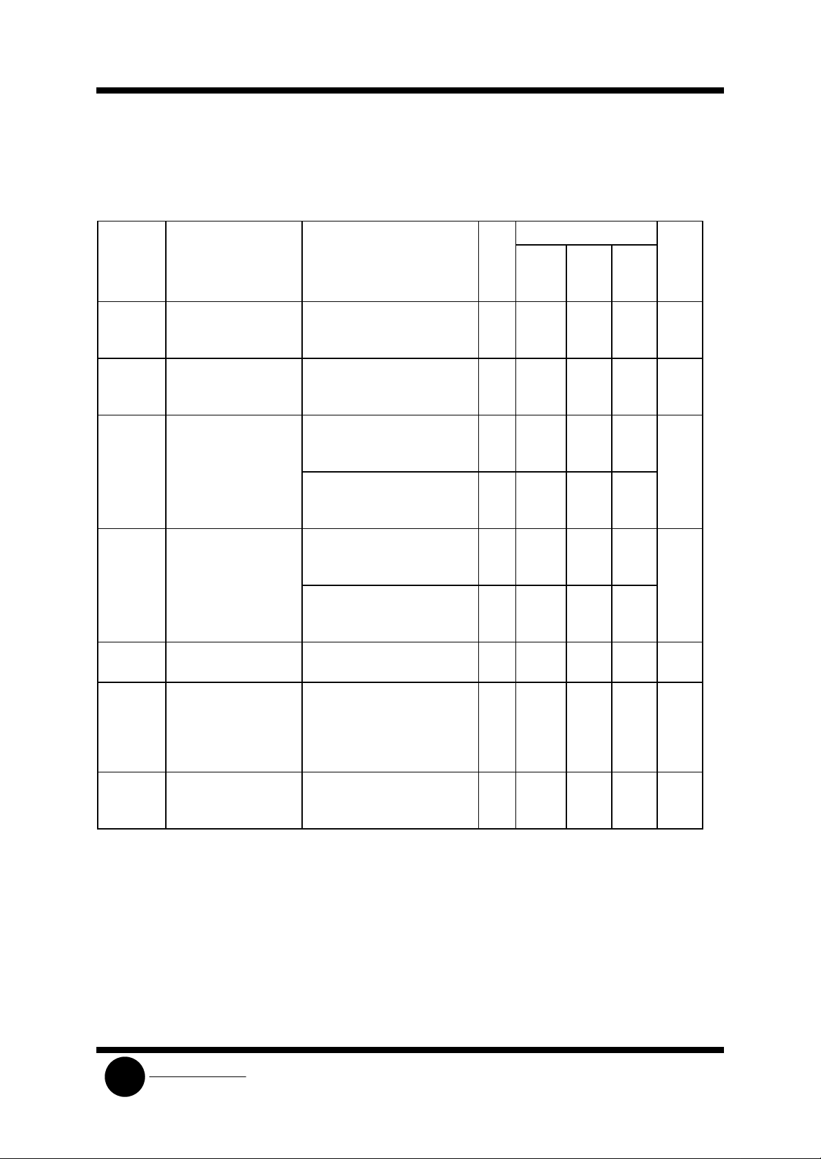
DC ELECTRICAL CHARACTERISTICS(Voltages Referenced to GND)
VCC Guaranteed Limit
Symbol Parameter Test Conditions V 25 °C
to
-55°C
VIH Minimum High-Level
Input Voltage
VIL Maximum Low -Level
Input Voltage
VOH Minimum High-Level
Output Voltage
VIN=VIH or VIL
VOL Maximum Low -Level
Output Voltage
VIN=VIH or VIL
IIN Maximum Input
Leakage Current
V
=0.1 V or VCC-0.1 V
OUT
I
≤ 20 µA
OUT
V
=0.1 V or VCC-0.1 V
OUT
I
≤ 20 µA
OUT
VIN=VIH or VIL
I
≤ 20 µA
OUT
I
≤ 6.0 mA
OUT
I
≤ 7.8 mA
OUT
VIN= VIL or VIH
I
≤ 20 µA
OUT
I
≤ 6.0 mA
OUT
I
≤ 7.8 mA)
OUT
VIN=VCC or GND
(Pins 1,2,3,21,22,and 23)
2.0
4.5
6.0
2.0
4.5
6.0
2.0
4.5
6.0
4.5
6.0
2.0
4.5
6.0
4.5
6.0
1.5
3.15
4.2
0.5
1.35
1.8
1.9
4.4
5.9
3.98
5.48
0.1
0.1
0.1
0.26
0.26
6.0 ±0.1 ±1.0 ±1.0 µA
≤85
°C
1.5
3.15
4.2
0.5
1.35
1.8
1.9
4.4
5.9
3.84
5.34
0.1
0.1
0.1
0.33
0.33
≤125
°C
1.5
3.15
4.2
0.5
1.35
1.8
1.9
4.4
5.9
3.7
5.2
0.1
0.1
0.1
0.4
0.4
Unit
V
V
V
V
IOZ Maximum Three-State
Leakage Current
ICC Maximum Quiescent
Supply Current
(per Package)
System Logic
SLS
Output in High-Impedance
State
VIN= V
V
IL
OUT=VCC
or V
IH
or GND,
I/O Pins
VIN=VCC or GND
I
=0µA
OUT
6.0 ±0.5 ±5.0 ±10 µA
6.0 8.0 80 160 µA
Page 4
SL74HC652
Semiconductor
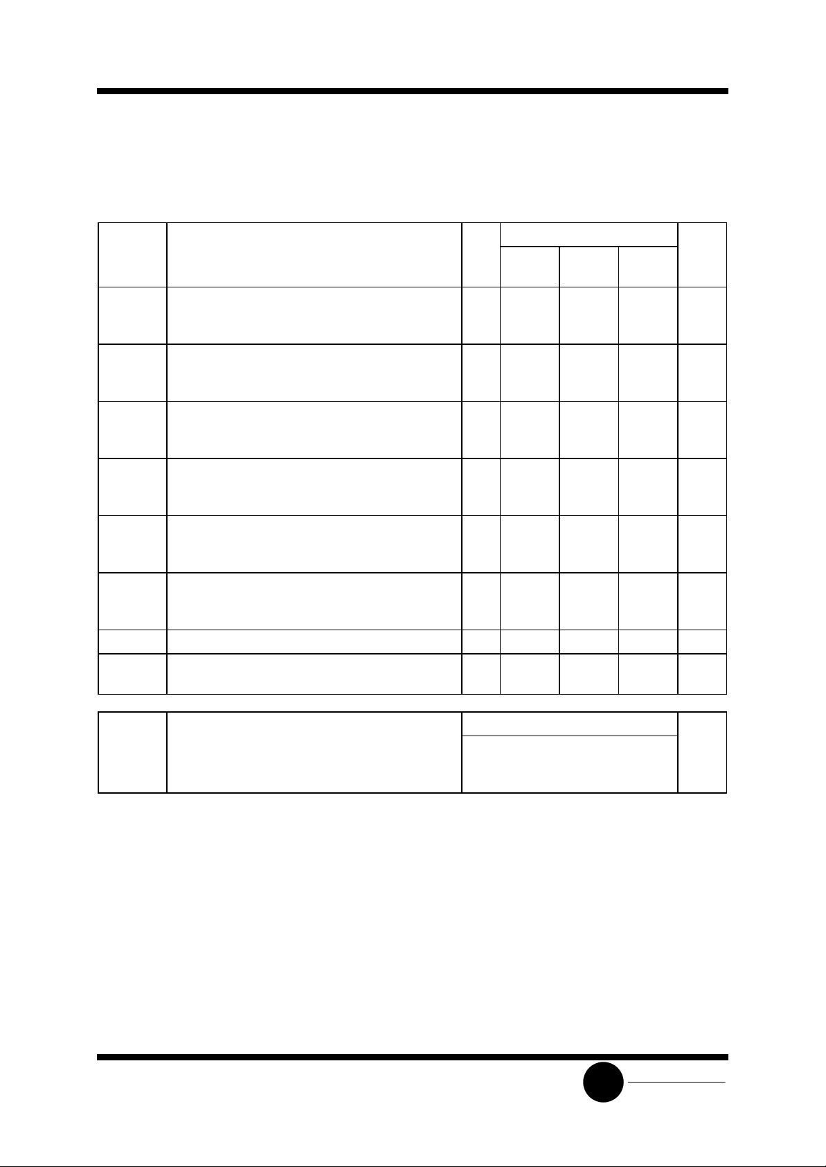
AC ELECTRICAL CHARACTERISTICS(C
=50pF,Input tr=tf=6.0 ns)
L
VCC Guaranteed Limit
Symbol Parameter V 25 °C to
≤85°C ≤125°C Unit
-55°C
t
, t
t
t
t
t
t
PLH
PLH
PLH
PLZ
PZL
TLH
Maximum Propagation Delay, Input A to Output B
PHL
(or Input B to Output A)
(Figures 2,3 and 9)
, t
Maximum Propagation Delay, A-to-B Clock to
PHL
Output B (or B-to-A Clock to Output A)
(Figures 1 and 9)
, t
Maximum Propagation Delay, A-to-B Source to
PHL
Output B (or B-to-A Source to Output A) (Figures
4 and 9)
, t
Maximum Propagation Delay , Direction or Output
PHZ
Enable to Output A or B
(Figures 5,6 and 10)
, t
Maximum Propagation Delay , Direction or Output
PZH
Enable to Output A or B
(Figures 5,6 and 10)
, t
Maximum Output Transition Time, Any Output
THL
(Figure 2)
2.0
4.5
6.0
2.0
4.5
6.0
2.0
4.5
6.0
2.0
4.5
6.0
2.0
4.5
6.0
2.0
4.5
6.0
180
36
31
240
48
41
220
44
37
170
34
29
180
36
31
60
12
10
225
45
38
300
60
51
275
55
47
215
43
37
225
45
38
75
15
13
270
54
46
360
72
61
330
66
56
255
51
43
270
54
46
90
18
15
ns
ns
ns
ns
ns
ns
CIN Maximum Input Capacitance - 10 10 10 pF
C
Maximum Three-State I/O Capacitance
OUT
- 15 15 15 pF
(Output in High-Impedance State
Power Dissipation Capacitance (Per Channel) Typical @25°C,VCC=5.0 V
CPD Used to determine the no-load dynamic power
consumption:
PD=CPDV
2
f+ICCVCC
CC
60 pF
SLS
System Logic
Page 5
SL74HC652
Semiconductor
TIMING REQUIREMENTS(Input t
VCC Guaranteed Limit
Symbol Parameter V 25 °C to-55°C ≤85°C ≤125°C Unit
tsu Minimum Setup Time, Input A to
A-to-B Clock (or Input B to B-to-A
Clock) (Figure 7)
th Minimum Hold Time, A-to-B Clock to
Input A (or B-to-A Clock to
Input B) (Figure 7)
tw Minimum Pulse Width, A-to-B Clock
(or B-to-A Clock)
(Figure 7)
tr, tf Maximum Input Rise and Fall Times
(Figures 2 and 3)
=6.0 ns)
r=tf
2.0
4.5
6.0
2.0
4.5
6.0
2.0
4.5
6.0
2.0
4.5
6.0
50
10
9
25
5
5
75
15
13
1000
500
400
65
13
11
30
6
5
95
19
16
1000
500
400
75
15
13
40
8
7
110
22
19
1000
500
400
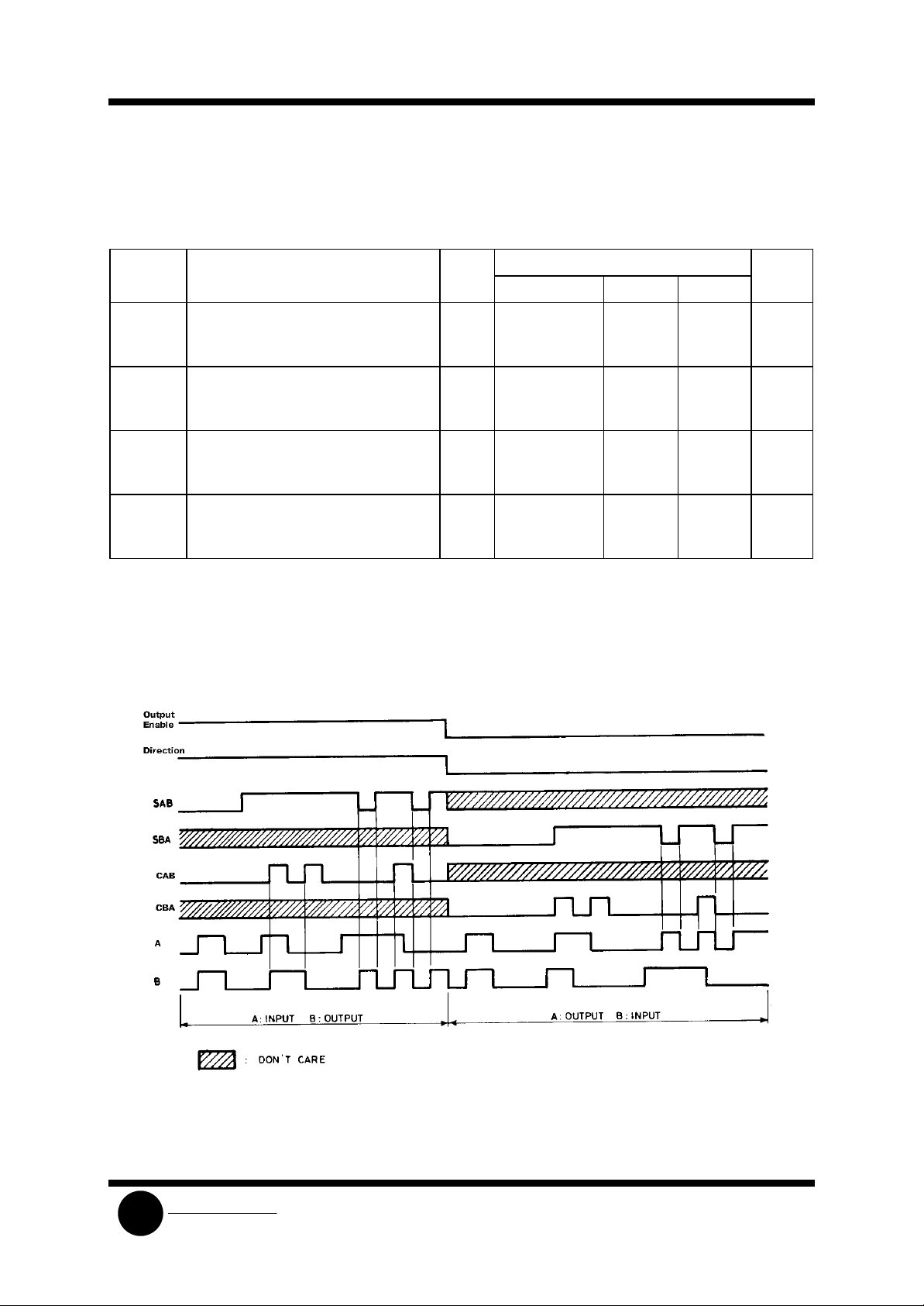
TIMING DIAGRAM
ns
ns
ns
ns
SLS
System Logic
Page 6
SL74HC652
Semiconductor
A bus. The data of the B bus are stored to
flops on low to high transition
A bus. The data of the B bus are stored to
flops on low to high transition
Dir. OE CAB CBA SAB SBA A B FUNCTION
INPUTS INPUTS Both the A bus and the B bus are inputs.
L H X X X X Z Z The output functions of the A and B bus
X X INPUTS INPUTS Both the A and B bus are used for inputs
OUTPUTS INPUTS The A bus are outputs and the B bus are
X* X X L L
L L X* X L L
X* X X H Qn X The data stored to the internal flip-flops,
X* X H H
INPUTS OUTPUTS The A bus are inputs and the B bus are
X X* L X L
H H X* L X L
X X* H X X Qn The data stored to the internal flip-flops
X* H X L
OUTPUTS OUTPUTS Both the A bus and the B bus are outputs
H L X X H H Qn Qn The data stored to the internal flip-flops
H H Qn Qn The output at the A bus are displayed at
X : DON’T CARE
Z : HIGH IMPEDANCE
Qn : THE DATA STORED TO THE INTERNAL FLIP-FLOPS BY MOST RECENT LOW TO HIGH TRANSITION
OF THE CLOCK INPUTS
*
: THE DATA AT THE A AND B BUS WILL BE STORED TO THE INTERNAL FLIP-FLOPS ON EVERY LOW TO
TRANSITION OF THE CLOCK INPUTS
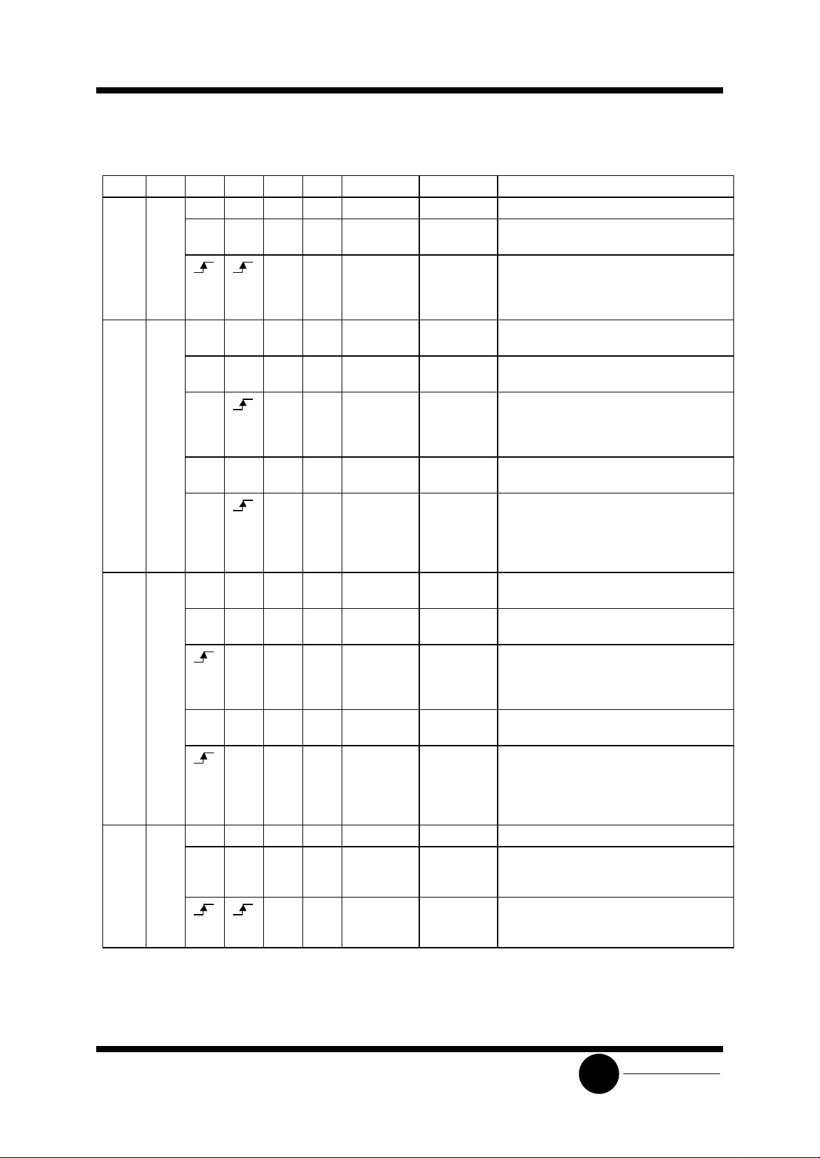
FUNCTION TABLE
L
H
H
L
H
H
H
H
L
H
H
L
L
H
L
H
L
H
are disabled.
to the internal flip-flops. Data at the bus
will be stored on low to high transition of
the clock inputs.
inputs.
The data at the B bus are displayed at the
A bus.
The data at the B bus are displayed at the
the internal flip-flops on low to high
transition of the clock pulse.
are displayed at the A bus.
The data at the B bus are stored to the
internal flipof the clock pulse. The states of the
internal flip-flops output directly to the A
bus.
outputs.
The data at the A bus are displayed at the
B bus.
The data at the B bus are displayed at the
the internal flip-flops on low to high
transition of the clock pulse.
are displayed at the B bus.
The data at the A bus are stored to the
internal flipof the clock pulse. The states of the
internal flip-flops output directly to the B
bus.
are displayed at the A and B bus
respectively.
the B bus, the output at the B bus are
displayed at the A bus respec.
SLS
System Logic
Page 7
SL74HC652
Semiconductor
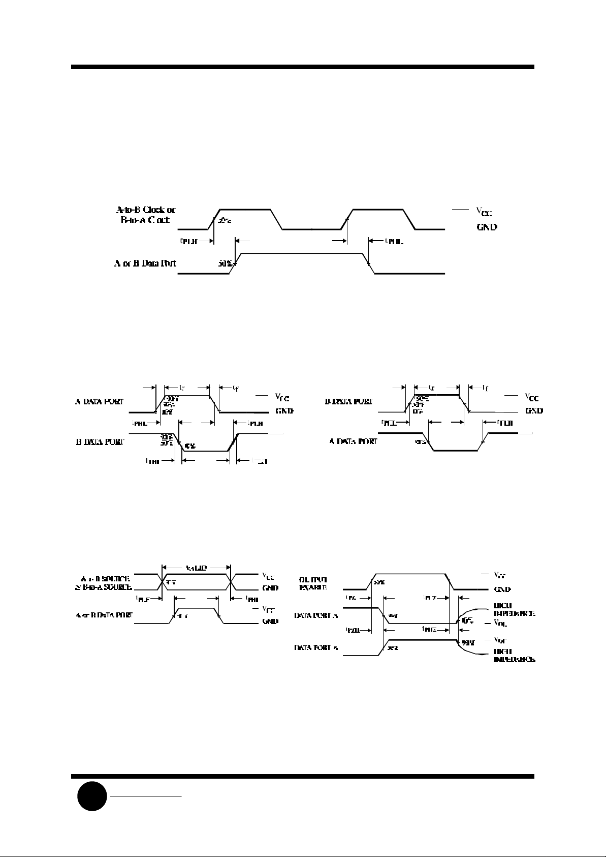
SWITCHING DIAGRAMS
Figure 1. Switching Waveforms
Figure 2. A Data Port = I nput, B Data Port = Output
Figure 3. A Data Port = Output, B Data Port = Input
SLS
Figure 4. Switching Waveforms Figure 5. Switching Waveforms
System Logic
Page 8
SL74HC652
Semiconductor
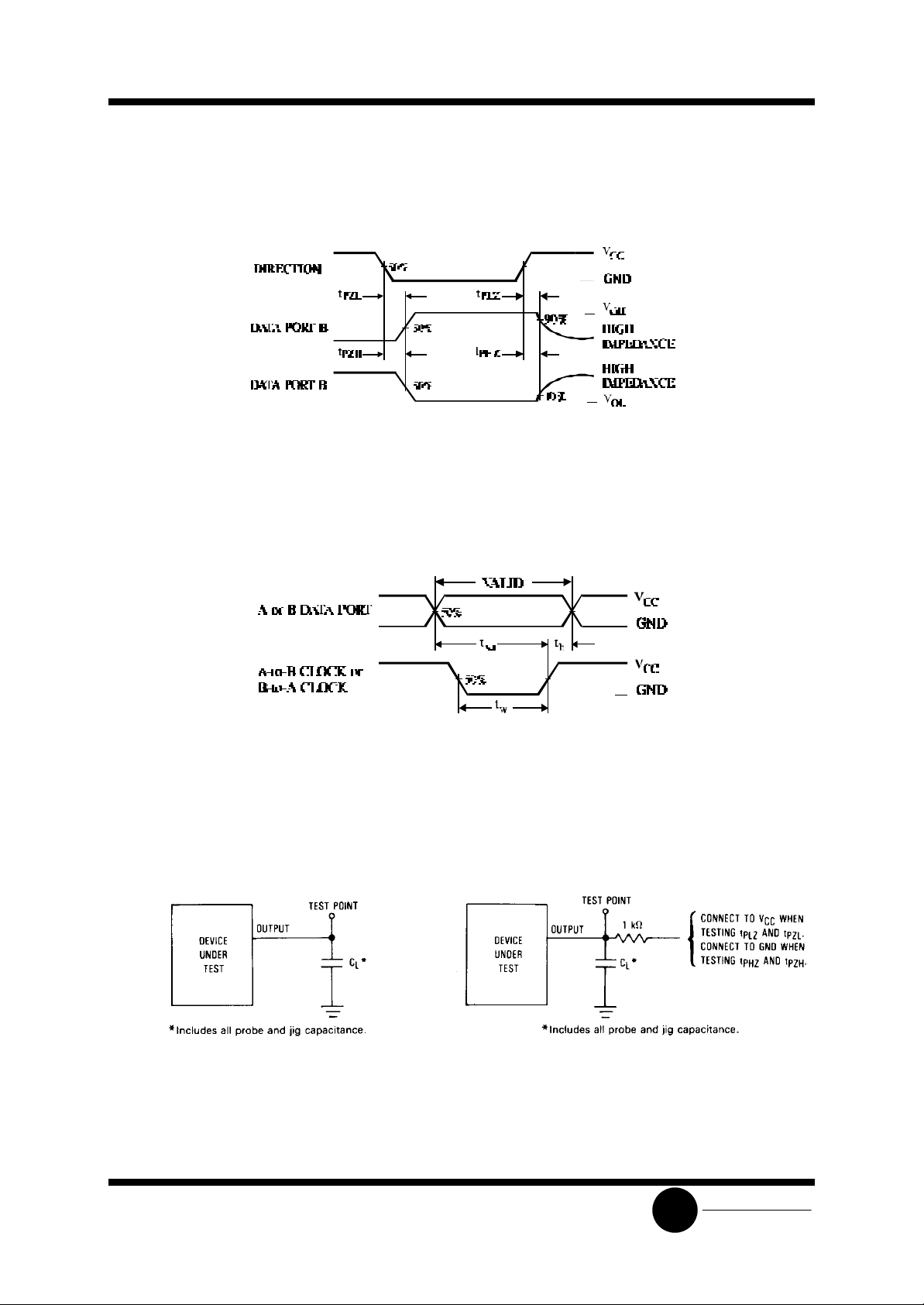
Figure 6. Switching Waveforms
Figure 7. Switching Waveforms
Figure 9. Test Circuit Figure 10. Test Circuit
SLS
System Logic
Page 9
SL74HC652
Semiconductor
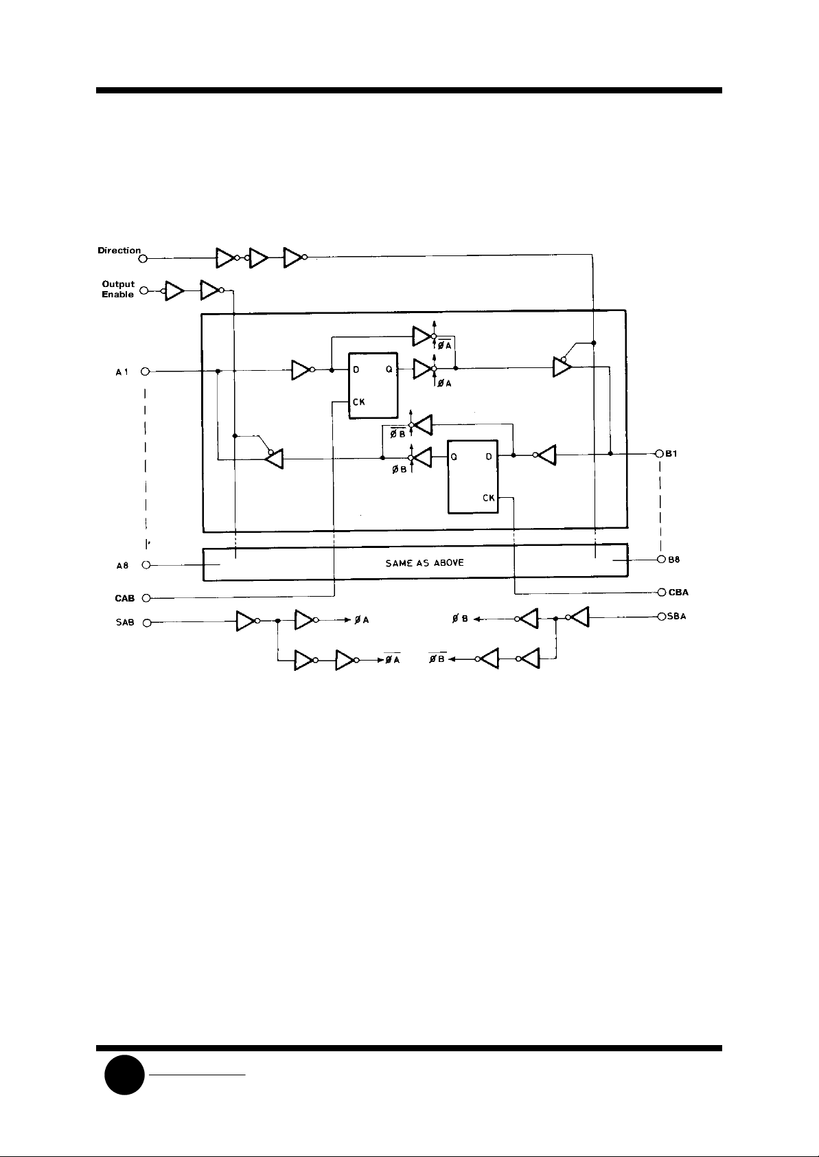
EXPANDED LOGIC DIAGRAM
SLS
System Logic
 Loading...