

Page 1

SL1925
Satellite Zero IF QPSK Tuner IC
Preliminary Information
Description
The SL1925 is a wideband quadrature converter operating
from 950 to 2150 MHz, intended primarily for application
in satellite tuners.
The device contains all elements necessary, with the
exception of local oscillator sustaining network, to fabricate
a high performance I(n-phase) & Q(uadrature) phase
splitter and downconverter optimised for systems
containing RF AGC gain control. The device allows for
systems containing higher power analog interferers. For
most applications RF tunable filtering is not essential.
The SL1925 is optimised for use with a low phase noise
synthesiser, a range of which are available from Mitel
Semiconductor. This will form a complete front end tuner
function for digital satellite receiver systems utilising DSP
derotation recovery.
The device includes a very high signal handling front end
with AGC, this provides for gain control, reference local
oscillator with output buffer, phase splitter with I and Q
mixers and baseband buffer amplifiers with external
interstage filtering.
Features
● Single chip system for direct quadrature down
conversion from L-band
● High signal handling capability for minimum
external component count application, requires
external RF AGC of 30dB
● Compatible with DSS and DVB system
requirements
● Excellent gain and phase match up to 30MHz
baseband
● High output referred linearity for low distortion and
multi channel application
● Fully balanced low radiation design
● Integral RF AGC amplifier
● Two selectable varactor tuned local oscillators
with buffered output for driving external
synthesiser loop
● ESD protection (Normal ESD handling procedures
should be observed)
Ordering Information
SL1925/KG/NP2S (Tubes)
SL1925/KG/NP2T (Tape and Reel)
Applications
● Satellite receiver systems
● Data communications systems
DS4955 Issue - 2.0 March 1999
Page 2
2
SL1925 Preliminary Information
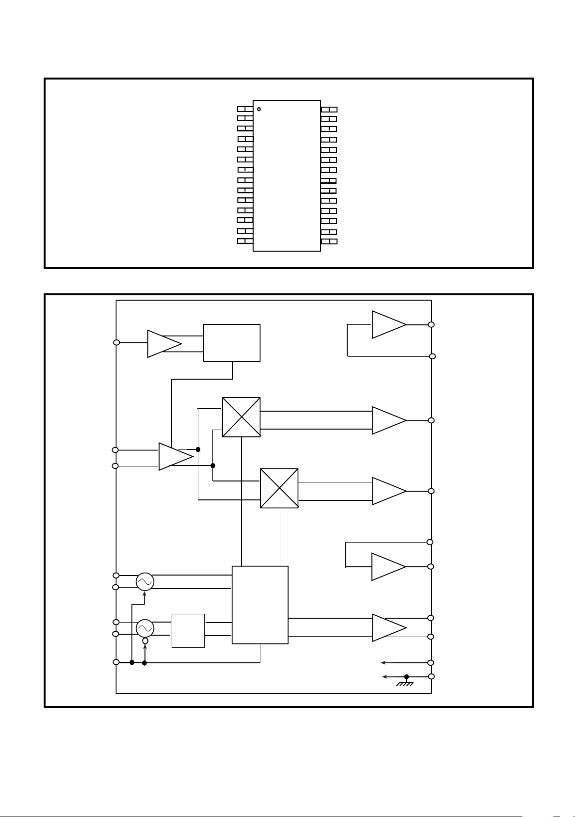
NP28
Figure 1 Pin connections
OPFI
OPFQ
Vcc
PSout
PSoutb
Vee
Tanks
Tanksb
Vee
Tankv
Tankvb
Vee
NC
Vcc
128
14
15
Vee
IPFI
Vee
Iout
LOsel
Vcc
RF
RFB
Vee
AGC
Qout
Vee
IPFQ
Vee
Figure 2 Block diagram
27
AGC
19
22
21
RF
RFB
9
10
Tankv
Tankvb
6
7
24
Tanks
Tanksb
LOsel
vcos
DIVIDE
BY 2
AGC
SENDER
0 DEG
25
Iout
IPFI
1
OPFI
14
OPFQ
16
IPFQ
18
Qout
3
PSout
4
PSoutb
2, 13, 23 Vcc
5, 8, 11, 15, 17, 20, 26, 28
Vee
90 DEG
vcov
FREQUENCY
AGILE
PHASE
SPLITTER
Page 3
3
Preliminary Information SL1925
Quick Reference Data
Characteristic Units
Operating range 950-2150 MHz
Input noise figure, DSB, maximum gain, 1500MHz 19 dB
Maximum conversion gain (assuming 6dB filter loss) >55 dB
Minimum conversion gain (assuming 6dB filter loss) <20 dB
IP32T input referred 113 dBuV
Converter input referred IM3, two tones at 97dBµV 30 dBc
IP22T input referred 140 dBuV
P1dB input referred 103 dBuV
Baseband amplifier Output limit voltage 2.0 V
Gain match up to 22 MHz 0.2 dB
Phase match up to 22 MHz 0.7 deg
Gain flatness up to 22 MHz 0.5 dB
Local oscillator phase noise across entire 950MHz to 2150MHz band:
SSB @ 10 kHz offset 80 dBc/Hz
Table 1
The required 950MHz to 2150MHz I and Q reference LO
frequencies for quadrature direct conversion are
generated by the on board oscillators named ‘vcos’ and
‘vcov’, and the phase splitter. Oscillator ‘vcos’ operates
nominally from 1900MHz to 3000MHz and is then divided
by two to provide 950MHz to 1500MHz. Oscillator ‘vcov’
operates nominally from 1400MHz to 2150MHz. Only
one oscillator is active at any time and selection is made
within the phase splitter under the control of the LOsel
input. Each oscillator uses an external varactor tuned
resonant network optimised for low phase noise with a
single varactor line control. A recommended application
circuit for the oscillators is shown in Figure 4. The LO
from the phase splitter drives a buffer whose outputs
‘PSout’ and ‘PSoutb’ can be used for driving an external
PLL control loop for the VCO’s. The typical LO phase
noise is shown in Figure 11.
The mixer outputs are coupled to baseband buffer
outputs ‘OPFI’ and ‘OPFQ’ which drive external band
limit filters. The output impedance of these buffers is
contained in Figure 12. The outputs of the filters are then
connected to the inputs ‘IPFI’ and ‘IPFQ’ of the baseband
channel amplifiers. The outputs ‘Iout’ and ‘Qout’ provide
for a low impedance drive and can be used with a
maximum load as in Figure 3. The output impedance of
this section is contained in Figure 13. An example filter
for application with 30MS/s systems is contained in
Figure 14.
All port peripheral circuitry for the SL1925 is shown in
Figure 15a and 15b.
The typical key performance data at 5V Vcc and 25°C
ambient are shown in the ‘QUICK REFERENCE DATA’
of Table 1.
Functional Description
The SL1925 is a wideband direct conversion quadrature
downconverter optimised for application in satellite
receiver systems. A block diagram is given in Figure 2
and shows the device to include a broadband RF
preamplifier with AGC control, two oscillator sustaining
amplifiers, a frequency agile 90° phase splitter, I Q
channel mixers and I Q channel baseband amplifiers.
The only additional elements required are an external
tank circuit for each oscillator, and baseband interstage
filters. To fabricate a complete tuner an RF AGC stage
offering +20dB to -10 dB of gain range and a 2.2 GHz
PLL frequency synthesiser are also required. An example
application is shown in Figure 16.
In normal application the first satellite IF frequency of
typically 950 to 2150 MHz is fed via the tuner RF AGC
stage to the RF preamplifier, which is optimised for
impedance match and signal handling. The RF
preamplifier is designed such that no tracking RF filter is
required and also allows for analog interferers at up to
10 dB higher amplitude. The converter RF input
impedance is shown in Figure 5. The amplifier signal is
then fed to an AGC stage providing a minimum of 35dB
AGC control, which together with the RF attenuator
provides a possible overall tuner dynamic range of
65dB, to allow for normal operating dynamic range and
MCPC systems. The signal is then split into two balanced
channels to drive the I and Q mixers. The AGC
characteristic, and gain variation of IIP3, IIP2, P1dB and
NF are contained in Figs. 6, 7, 8, 9 and 10 respectively.
Page 4
4
SL1925 Preliminary Information
Figure 3 Baseband output load condition
15pF
100Ω
1kΩ
Note: Stripline width =0.44mm,dimensions are approximate.
Marker Freq (MHz) Zreal Ω Zimag Ω
1 950 90 -18
2 1350 76 -15
3 1750 63 -35
4 2150 46 -29
Figure 5 Converter RF input impedance (typical)
0.50.2 10
+j0.2
+j0.5
+j1
+j2
+j5
2 5
–j5
–j2
–j1
–j0.5
–j0.2
STOP 2 500
START 700
X
X
X
X
X
1
2
3
4
Normalised to 50Ω
MHz
MHz
Figure 4 Local oscillator application circuit
"vcov"
1T379
1T379
BB811
BB811
1kΩ
Vcnt
6.15MM STRIPLINE
6.15MM STRIPLINE
9MM STRIPLINE
9MM STRIPLINE
6
7
9
10
Tanks
Tanksb
Tankv
Tankvb
"vcos"
1kΩ
Page 5
5
Preliminary Information SL1925
Figure 6 Converter gain variation with AGC voltage (typical)
-20.0
-10.0
0.0
10.0
20.0
30.0
40.0
50.0
0.0 0.5 1.0 1.5 2.0 2.5 3.0 3.5 4.0 4.5 5.0
AGC control voltage (V)
Converter conversion gain (dB)
30dB minimum, AGC <1V
-5dB maximum, AGC >4V
90
95
100
105
110
115
120
-6 -1 4 9 14 19 24 29 34
Converter gain setting (dB)
Converter input referred IP3 (dBuV)
Figure 7 Converter input referred IP3 variation with gain setting (typical)
Page 6
6
SL1925 Preliminary Information
100
105
110
115
120
125
130
135
140
-6 -1 4 9 14 19 24 29 34
Converter gain setting (dB)
Converter input referred IP2 (dBuV)
Figure 8 Converter input referred IP2 variation with gain setting (typical)
80
85
90
95
100
105
110
-6 -1 4 9 14 19 24 29 34
Converter gain setting (dB)
Converter RF input level at P1dB (dBuV)
Figure 9 Converter input referred 1dB gain compression, P1dB (typical)
Page 7

7
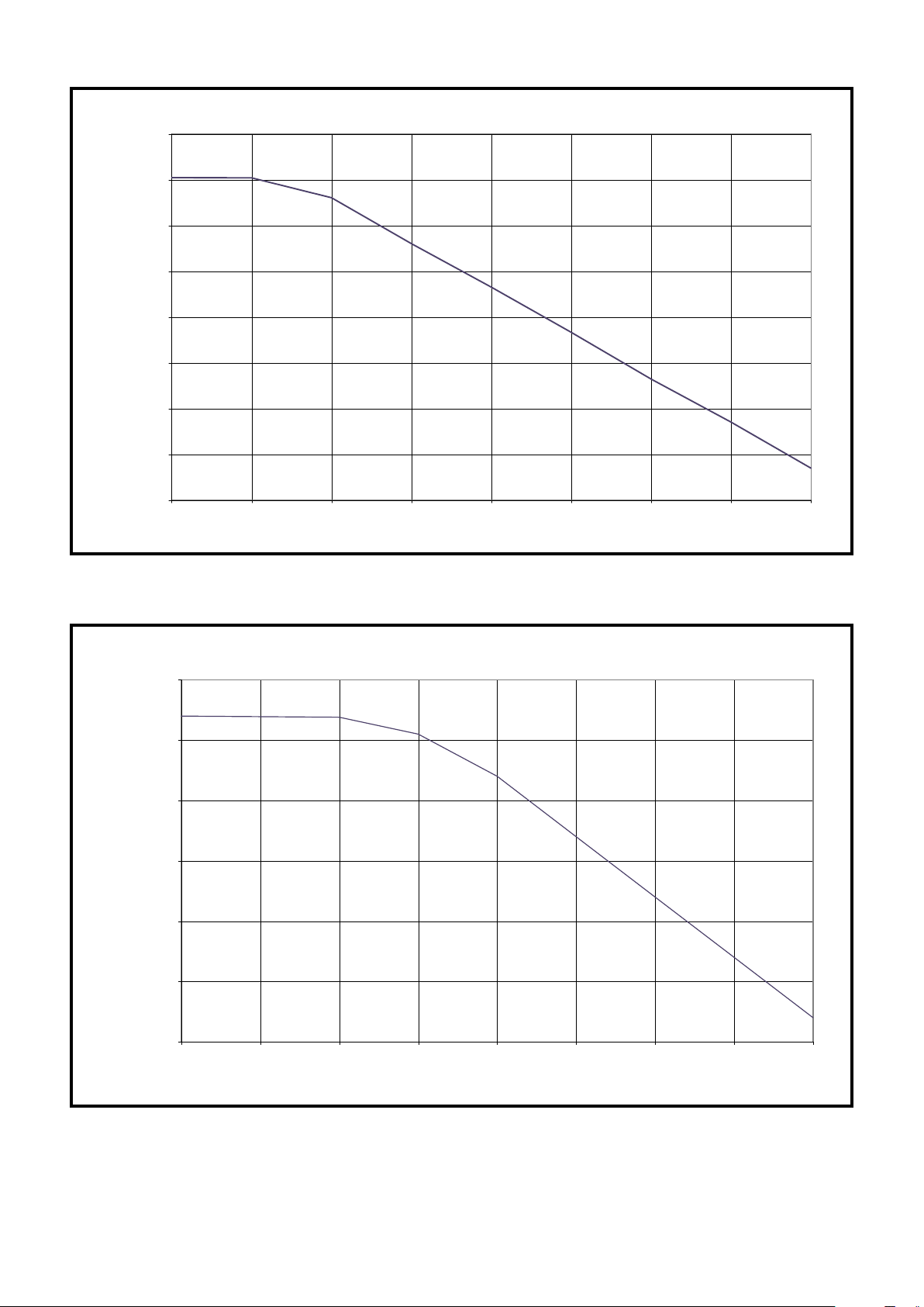
Preliminary Information SL1925
10
20
30
40
50
60
20 25 30 35 40 45 50 55
System gain (dB)
Noise Figure (dB)
Figure 10 Noise figure variation with gain setting (typical)
Page 8

8
SL1925 Preliminary Information
-90
-88
-86
-84
-82
-80
-78
-76
-74
-72
-70
950 1150 1350 1550 1750 1950 2150
LO Frequency (MHz)
Phase noise @10kHz offset (dBc/Hz)
vcos enabled
vcov enabled
Figure 11 LO phase noise variation with frequency (typical)
Figure 12 Converter output impedance, OPFI and OPFQ (typical)
Marker Freq (MHz) Zreal Ω Zimag Ω
1 1 24 0.5
210 2511
330 3029
0.50.2 10
+j0.2
+j0.5
+j1
+j2
+j5
2 5
–j5
–j2
–j1
–j0.5
–j0.2
STOP 2 500
START 700
Normalised to 50Ω
3
x
x
x
1
2
10kHz
50MHz
Page 9

9
Preliminary Information SL1925
Figure 13 Baseband output impedance, Iout and Qout (typical)
Marker Freq (MHz) Zreal Ω Zimag Ω
1 1 11.4 3.4
2 10 9.6 0.2
3 30 7.3 4.7
Figure 14 Example baseband interstage filter for 30MS/s application
0.5 10
+j0.2
+j0.5
+j1
+j2
+j5
2 5
–j5
–j2
–j1
–j0.5
–j0.2
STOP 50MHz
START 10kHz
X
X
X
X
1
2
3
Normalised to 50Ω
OPFI / OPFQ
100nF
1kΩ
1kΩ
IPFI / IPFQ
3.9pF
Page 10

10
SL1925 Preliminary Information
LO OUTPUT
LO OUTPUTB
V
cc
V
REF4
AGC
12K
CONTROL
2K
V
REF 3
V
cc
IF-OP-SEL
V
REF 2
1K 1K
TANK
TANKB
RF INPUTS
OPFI & OPFQ
Converter RF inputs (pins 21, 22)
Oscillator select input (pin 24)
Oscillator inputs (pins 6, 7, and 9,10)
Converter outputs (pins 1, 14)
Prescaler buffer drive (Pins 3,4)
AGC input (pin 19)
PSout
PSoutb
Figure15a Input/Output interface circuits
LOsel
Page 11

11
Preliminary Information SL1925
Iout
and
Qout
Baseband amplifier inputs (pins 16,27)
Baseband outputs (pins 18, 25)
Figure 15b Input/Output interface circuits (continued)
IPFI
and
IPFQ
BIAS
Page 12

12
SL1925 Preliminary Information
Electrical Charqacterisitics
These characteristics are guaranteed by either production test or design. They apply within the specified
ambient temperature and supply voltage unless otherwise stated.
T
amb
= -20°C to + 70°C, Vee= 0V, Vcc = 4.75V to 5.25V. Desired channel at fc MHz
Characteristic
Value
Min
Typ Max
Units
Conditions
Pin
Supply current, Icc 2,13,23 130 175 mA
RF input operating frequency 21,22 950 2150 MHz
SYSTEM All system specification items should be
read in conjunction with Note 1.
System noise figure, DSB 21,22 19 dB Maximum gain, AGC = 1V
Variation in system NF with gain 21,22 -1 dB/dB See Figure 10
adjust
System input referred IP2 135 140 dBµV See Note 2.
System input referred IP3 110 113 dBµV See Note 3.
System conversion gain Terminated voltage conversion gain into
load as in Figure 3.
AGC monotonic from Vee to Vcc, see
Figure 6
Minimum AGC gain 20 dB AGC = 4.0V, 950MHz
Maximum AGC gain 59 dB AGC = 1.0V, 950MHz
Gain Roll off 5 dB 950MHz to 2150MHz
System I/Q gain match 18,25 -1 +1 dB Excluding interstage filter stage
System I/Q phase balance 18,25 -3 3 deg Excluding interstage filter stage
System I & Q channel in band 18,25 1 dB Excluding interstage filter stage
ripple
LO 2nd harmonic interference level -50 dBc See Note 5
LNA 2nd harmonic interference -35 dBc See Note 6
level
All other spurii on I & Q outputs 18,25 78 dBµV Within 0 →100MHz band, under all gain
settings, RF input set to deliver 108dBµV
at baseband outputs
CONVERTER
Converter input impedance 21,22 75 Ω See Figure 5
Converter input return loss 21,22 10 12 dB
Converter input referred IP2 21,22 121 130 dBµV See Note 4
Converter input referred IP3 21,22 110 112 dBµV See Note 4
Converter input referred IM2 21,22 -33 -24 dBc See Note 4
Converter input referred IM3 21,22 -30 -26 dBc See Note 4
Converter input referred 1dB 21,22 See Figure 9
gain compression (P1dB)
Converter conversion gain Terminated voltage conversion gain in
load as in Figure 3.
Minimum AGC gain -5 dB AGC = 4.0V
Maximum AGC gain 30 dB AGC = 1.0V
AGC gain control slope variation Monotonic from Vee to Vcc, see Figure 6
AGC control input current 19 -250 250 µA AGC bandwidth 100kHz
Page 13

13
Preliminary Information SL1925
Electrical Characteristics (continued)
These characteristics are guaranteed by either production test or design. They apply within the specified
ambient temperature and supply voltage unless otherwise stated.
T
amb
= -20°C to + 70°C, Vee= 0V, Vcc = 4.75V to 5.25V. Desired channel at fc MHz
Characteristic
Value
Min
Typ Max
Units
Conditions
Pin
Converter output impedance 1,14 25 50 Ω 0.1 to 30MHz. See Figure 12
Converter output limiting 1,14 0.5 1.2 Vp-p No Load
Converter bandwidth 1dB 40 MHz No Load
Converter output roll off 1,14 6 dB/oct
Oscillator vcos operating range 6,7 1900 3000 MHz Giving LO = 950MHz to1500MHz
Tanks/Tanksb Application as in Figure 4.
Oscillator vcov operating range, 9,10 1450 2150 MHz Application as in Figure 4.
Tankv/Tankvb
Local oscillator SSB phase noise 6,7 -80 -76 dBc/Hz @ 10kHz offset PLL loop BW < 1kHz,
application as Figure 4. Measured at
baseband outputs of 10MHz
LO leakage to converter input 21,22 59 69 dBµV
LOsel low voltage 24 0.6 V Oscillator vcos enabled
LOsel high voltage 24 Vcc-0.7 V Oscillator vcov enabled
LOsel low current 24 -50 µA
LOsel high current 24 200 µA
Prescaler output drive 3,4 88 dBµV Single ended into 50Ω. Synthesiser
should be driven differentially
Prescaler output impedance 3,4 50 Ω
Prescaler output return loss 3,4 8 dB
BASEBAND AMPLIFIERS
Baseband amplifier input 16,27 0.1 -30MHz bandwidth
impedance
Resistance 10 kΩ
Capacitance 5 pF
Baseband amplifier input referred 16,27 94 97 dBµV See Note 7
IP3
Baseband amplifier input referred 16,27 99 111 dBµV See Note 7
IP2
Baseband amplifier input referred 16,27 -40 -34 dBc See Note 7
IM3
Baseband amplifier input referred 16,27 -34 -22 dBc See Note 7
IM2
Baseband amplifier input referred 16,27 84 dBµV Terminated voltage gain into load as in
1dB compression (P1dB) Figure 3.
Baseband amplifier gain 16,18 30 dB Terminated voltage gain into load as in
27,25 Figure 3
Page 14

14
SL1925 Preliminary Information
Electrical Characteristics (continued)
These characteristics are guaranteed by either production test or design. They apply within the specified
ambient temperature and supply voltage unless otherwise stated.
T
amb
= -20°C to + 70°C, Vee= 0V, Vcc = 4.75V to 5.25V. Desired channel at fc MHz
Characteristic
Value
Min Typ Max
Units
Conditions
Pin
Baseband amplifier output 18,25 20 Ω
impedance
Baseband amplifier output 18,25 2.0 Vp-p pk-pk level at hard clipping.
limiting Load as in Figure 3.
Baseband amplifier 1dB 18,25 40 MHz Load as in Figure 3.
bandwidth
Baseband output roll off 18,25 6 dB/oct Above 3dB point, no load
Notes : 1. Systems specifications refer to total cascaded system of front end converter/AGC stage and baseband amplifier stage
with nominal 6dB pad as interstage filter and load impedance as in Figure 3.
2. AGC set to deliver output amplitude of 108dBµV on desired channel, input frequency fc and amplitude of 79dBµV, with
two interferers of frequencies fc+146 and fc+155MHz at 97dBµV generating output intermodulation spur at 9MHz.
40MHz 3dB bandwidth interstage filter included.
3. AGC set to deliver output amplitude of 108dBµV on desired channel, input frequency fc and amplitude 79 dBµV, with
two interferers of frequencies fc+110 and fc+211MHz at 97 dBµV generating output intermodulation spur at 9MHz.
40MHz 3dB bandwidth interstage filter included.
4. Two tones within RF operating frequency range at 97dBµV, conversion gain set at 4dB.
5. The level of 2.01GHz downconverted to baseband relative to 1.01 GHz with the oscillator tuned to 1 GHz, measured
with no input filtering.
6. The level of second harmonic of 1.01 GHz input at -25 dBm downconverted to baseband relative to 2.01 GHz at -40 dBm
with the oscillator tuned to 2 GHz, measured with no input filtering.
7. Two tones within operating frequency range at 77dBµV.
Characteristic
Value
Min
Max
Units
Conditions
Pin
Absolute Maximum Ratings
All voltages are referred to Vee at 0V (pins 5,8,11,15,17,20,26,28)
Supply Voltage, Vcc 2,13,23 -0.3 7 V Transient condition only
PSout &PSoutb DC offset 3,4 Vcc-3.0 Vcc+0.3 Vp-p
RF & RFB input voltage 21,22 2.5 Vp-p AC coupled, transient conditions only
All other I/O ports DC offset 1,6,7,9 -0.3 Vcc+0.3 V
10,12
14,16
18,19
24,25,27
Storage Temperature -55 +150 °C
Junction Temperature +150 °C
NP28 package
Thermal resistance
Chip to ambient 85 °C/W
Chip to case 20 °C/W
Power consumption at 5.25V 893 mW
ESD protection All 4 kV Mil Std-883 latest revision method 3015
class 1
Page 15

15
Preliminary Information SL1925
SL1925 Demo Board
The demo board contains an SL1925 direct conversion
IC and SP5769 synthesiser. Reference to the
specifications for each device may be required in
conjunction with these notes.
The board contains all components necessary to
demonstrate operation of the SL1925. The schematic
and PCB layout of the board are shown in figures 16, 17
and 18. The SP5769 synthesiser is provided to control
each of the oscillators of the SL1925.
Supplies
The board must be provided with the following supplies:
5V for the synthesiser, 30V for the varactor line and 5V
for the SL1925.
The supply connector is a 5 pin 0.1” pitch pin header.
The order of connections is 5V - GND - 30V - GND - 5V
I2C Bus Connections
The board is provided with a RJ11 I2C bus connector
which feeds directly to the SP5769 synthesiser. This
connects to a standard 4 way cable which is supplied
with the interface box.
Operating Instructions
1. Software
Use the Mitel Semiconductor synthesiser software. Pull
down the I2C bus section menu then select the SP5769.
It is suggested that the charge pump setting 130uA is
used, and the reference divider is set to 32. These
settings give a small loop bandwidth (i.e. 100’s Hz),
which allows detailed phase noise measurements of the
oscillators to be taken, if desired.
2. VCO control
The two VCO’s are selected by toggling port P1 on the
synthesiser which in turn toggles the LOsel input of the
SL1925.
VCOS is switched on (and hence VCOV off) by clicking
P1 on - a tick will appear.
VCOS oscillates at twice the LO frequency (lower band)
and is then divided by two to provide the required LO
frequency in the range 950MHz to 1500MHz
approximately.
VCOV is switched on (and hence VCOS off) by clicking
P1 off - no tick.
VCOV oscillates at the LO frequency (upper band) in the
range 1450MHz to 2150MHz approximatley.
3. AGC control
The AGC input of the SL1925 which determines the
conversion gain should be controlled by application of an
external voltage to the AGC pin, TP1.
Caution: Care should be taken to ensure the chip is
powered ON when +ve voltages are applied to the AGC
input so as to avoid powering the chip up via the ESD
protection diode of the AGC input. It is recommended
that a low current limit is set on the external source used.
4. Free running the VCO’s
Select the required VCO using port P1 and then using
the software choose an LO frequency which is above the
maximum frequency capability of the oscillator. 3GHz
is suggested for both oscillators. Under this condition the
varactor control voltage is pumped to its maximum
value, i.e. to the top of the band. The oscillator frequency
may be manually tuned by varying the 30V supply.
Page 16

16
SL1925 Preliminary Information
Figure 16
SL1925 L BAND QUADRATURE DOWNCONVERTERTitle:
MITEL
OP FI1Vcc2PSout3PSoutb4Vee
5
Tanks6Tanksb7Vee8Tankv9Tankvb10Vee
11
NC12Vcc13OP FQ
14
Vee
15
IP FQ
16
Vee
17
Q OUT
18
AGC
19
Vee
20
RF inB
21
RF inA
22
Vcc
23
LO Sel
24
I OUT
25
Vee
26
IP FI
27
Vee
28
IC1
SL1925
C26
100nF
R4
1K
R3
1K
C25
100nF
5V
5V
5V
C14
1nF
C13
1nF
L1
L2
L3
L4
VD1
1T379
VD2
1T379
VD3
BB811
VD4
BB811
C23
100nF
R1
1K
R2
1K
C24
100nF
C6
220nF
C5
220nF
C16 1nF
C2 1nF
C1 1nF
R102
120R
PORT P1
8
PORT P0
9
ADDRESS
10
REF/COMP
11
RF IP
13
Vee
15
RF IP
14
CH PUMP1XTAL CAP
2
XTAL3SDA4SCL5P3/LL6P2
7
Vcc
12
DRIVE
16
IC2
SP5769
C60
150pF
C30
82pF
X1
4MHz
R16
10K
T1
BCW31
C31
15nF
C32
68pF
R7
13K
5V Synth
R8
22K
R10
1K
R19
1K
R9
15K
C39
2n2
C4
3p9
C3
3p9
C50
100nF
C51
100pF
C42
100pF
C44
100pF
+
C41
4u7
C47
100pF
C43
100nF
C49
100nF
C33
100nF
R5
100R
SMA3
I OUT
C80
15pF
R18
1K
R100
0R
123
J4
SMA5
IP/OP FI
TP1 Ext AGC Volts
SMA1
RF IN
R6
100R
SMA2
Q OUT
C81
15pF
R17
1K
R101
0R
123
J2
SMA6
IP/OP FQ
SDA5
3
5V0
4
GND
5
SCL5
6
J3
I2C BUS
C37
100pF
C38
100pF
5V
+
C52
4u7
12345
J1
DC Power
30V
5V Synth
C34
100nF
LO SELECT
LO SELECT
PSCb
PSCb
PSCa
PSCa
LINK INFORMATION
2-3 FILTER INPUT
1-2 FILTER OUTPUT
LINK INFORMATION
2-3 FILTER INPUT
1-2 FILTER OUTPUT
STRIPLINE DIMENSIONS
L1 & L2 6.0mm X 0.44mm
L3 & L4 8.0mm X 0.44mm
APPROXIMATE
L1 & L2 6.15mm X 0.44mm
L3 L4 9.0mm X 0.44mm
Page 17

17
Preliminary Information SL1925
Figure 17 Top View
Page 18

18
SL1925 Preliminary Information
Figure 18 Bottom view
Page 19

Page 20

M Mitel (design) and ST-BUS are registered trademarks of MITEL Corporation
Mitel Semiconductor is an ISO 9001 Registered Company
Copyright 1999 MITEL Corporation
All Rights Reserved
Printed in CANADA
TECHNICAL DOCUMENTATION - NOT FOR RESALE
World Headquarters - Canada
Tel: +1 (613) 592 2122
Fax: +1 (613) 592 6909
North America Asia/Pacific Europe, Middle East,
Tel: +1 (770) 486 0194 Tel: +65 333 6193 and Africa (EMEA)
Fax: +1 (770) 631 8213 Fax: +65 333 6192 Tel: +44 (0) 1793 518528
Fax: +44 (0) 1793 518581
http://www.mitelsemi.com
Information relating to products and services furnished herein by Mitel Corporation or its subsidiaries (collectively “Mitel”) is believed to be reliable. However, Mitel assumes no
liability for errors that may appear in this publication, or for liability otherwise arising from the application or use of any such information, product or service or for any infringement of
patents or other intellectual property rights owned by third parties which may result from such application or use. Neither the supply of such information or purchase of product or
service conveys any license, either express or implied, under patents or other intellectual property rights owned by Mitel or licensed from third parties by Mitel, whatsoever.
Purchasers of products are also hereby notified that the use of product in certain ways or in combination with Mitel, or non-Mitel furnished goods or services may infringe patents or
other intellectual property rights owned by Mitel.
This publication is issued to provide information only and (unless agreed by Mitel in writing) may not be used, applied or reproduced for any purpose nor form par t of any order or
contract nor to be regarded as a representation relating to the products or services concerned. The products, their specifications, services and other information appearing in this
publication are subject to change by Mitel without notice. No warranty or guarantee express or implied is made regarding the capability, performance or suitability of any product or
service. Information concerning possible methods of use is provided as a guide only and does not constitute any guarantee that such methods of use will be satisfactory in a specific
piece of equipment. It is the user’s responsibility to fully determine the performance and suitability of any equipment using such information and to ensure that any publication or
data used is up to date and has not been superseded. Manufacturing does not necessarily include testing of all functions or parameters. These products are not suitable for use in
any medical products whose failure to perform may result in significant injury or death to the user. All products and materials are sold and services provided subject to Mitel’s
conditions of sale which are available on request.
 Loading...