

Datasheet Si3211-KT, Si3212-BT, Si3212-KT, Si3210-BT, Si3210-KT Datasheet (Silicon Laboratories)
...Page 1
Si3210/Si3211/Si3212
S
T
PROSLIC™ PROGRAMMABLE CMOS SLIC/CODEC
WITH RINGING/BATTERY VOLTAGE GENERATION
Features
Performs all BORSCHT Functi ons
Ideal for Short Loop Appl ications
(5 REN at 2 kft, 3 REN at 4 kft)
Low Voltage CMOS
Package: 38-Pin TSSOP
Compliant with Relevant LSSGR and
CCITT Specifications
Battery Voltage Generated Dynamically
with On-Chip DC-DC Converter
Controller (Si 3210 only)
5 REN Ringing Generator
Programmable Frequency, Amplitude,
Waveshape, and Cadence
Programmable AC I mpedance
A-Law/µ-Law, Linear PCM Companding
On-Hook Tr ansmission
Applications
Terminal Adaptors
Cable Telephony
PBX/Key Systems
Description
The ProSLIC™ is a low-voltage CMOS device that integrates SLIC, codec, and
battery generation functionality into a complete analog telephone interface. The
device is ideal for short loop applications such as terminal adaptors, cable telephony,
and wireless local loop. Th e ProSLIC is powered with a single 3.3 V or 5 V supply.
The Si3210 generates battery voltages dynamically usin g a software program mable
dc-dc converter from a 3.3 V to 35 V supply; negative high-voltage supplies are not
needed. All high voltage functions are performed locally with a few low cost discrete
components. The device is available in a 38- pin TSSOP and interfaces directly to
standard SPI and PCM bus digital interfaces.
Functional Block Diagram
Programmable Constant Current
Feed (20–41 mA)
Programmable Loop Closure and
Ring Trip Thresholds with Debouncing
Loop or Ground S tart Operation and
Polarity Battery Reversal
Continuous Line V olt age and Current
Monitoring
DTMF Decoder
Dual Tone Generator
SPI and PCM Bus Digital Interf aces
with Programmable Interrupt for
Control and Data
3.3 V or 5 V Operation
Multiple Loopback Modes for Testing
Pulse Metering
FSK Caller ID Generation
Wireless Local Loop
Voice Ov er IP
Integrated Access Devices
Ordering Inform ati on
See page 118.
Pin Assignments
Si3210/11/12
CS
1
INT
DRX
DTX
IREF
2
3
4
5
6
7
8
9
10
11
12
13
14
15
16
17
18
19
PCLK
FSYNC
RESET
DCH/DIO1
SDCL/DIO2
VDDA1
CAPP
QGND
CAPM
STIPDC
SRINGDC
STIPE
SVBAT
SRINGE
ProSLIC
38
37
36
35
34
33
32
31
30
29
28
27
26
25
24
23
22
21
20
SCLK
SDI
SDO
SDITHRU
DCDRV/DCSW
DCFF/DOU
TEST
GNDD
VDDD
ITIPN
ITIPP
VDDA2
IRINGP
IRINGN
IGMP
GNDA
IGMN
SRINGAC
STIPAC
RESETINT
CS
SCLK
SDO
SDI
DTX
DRX
FSYNC
PCLK
Control
Interface
PCM
Interface
PLL
CompressionExpansion
Attenuation/
Attenuation/
Si3210/11/12
DTMF
Decode
Gain/
Filter
Tone
Generator
Gain/
Filter
Line
Status
A/D
Program
Hybrid
D/A
DC-DC Converter Controller
(Si3210 only)
Line
Feed
Control
Z
S
Low Cost
External
Discretes
Patents pending
TIP
RING
Preliminary Rev. 1.11 9/ 01 Copyright © 2001 by Silicon Labora tories Si3210-DS111
This in formation applies to a product under devel opment. I ts characteristics and specifications are subject to change without notice.
Page 2

Si3210/Si3211/Si3212
2 Preliminary Rev. 1.11
Page 3

Si3210/Si3211/Si3212
TABLE OF CONTENTS
Section Page
Electrical Specifications . . . . . . . . . . . . . . . . . . . . . . . . . . . . . . . . . . . . . . . . . . . . . . . . . 4
Functional Description . . . . . . . . . . . . . . . . . . . . . . . . . . . . . . . . . . . . . . . . . . . . . . . . . . 21
Linefeed Interface . . . . . . . . . . . . . . . . . . . . . . . . . . . . . . . . . . . . . . . . . . . . . . . . . . . 21
Battery Voltage Generation and Switching . . . . . . . . . . . . . . . . . . . . . . . . . . . . . . . . 27
Tone Generation . . . . . . . . . . . . . . . . . . . . . . . . . . . . . . . . . . . . . . . . . . . . . . . . . . . . 30
Ringing Generation . . . . . . . . . . . . . . . . . . . . . . . . . . . . . . . . . . . . . . . . . . . . . . . . . . 33
Pulse Metering Generation . . . . . . . . . . . . . . . . . . . . . . . . . . . . . . . . . . . . . . . . . . . . 37
DTMF Detection . . . . . . . . . . . . . . . . . . . . . . . . . . . . . . . . . . . . . . . . . . . . . . . . . . . . . 38
Audio Path . . . . . . . . . . . . . . . . . . . . . . . . . . . . . . . . . . . . . . . . . . . . . . . . . . . . . . . . . 39
Two-Wire Impedance Matching . . . . . . . . . . . . . . . . . . . . . . . . . . . . . . . . . . . . . . . . . 42
Clock Generation . . . . . . . . . . . . . . . . . . . . . . . . . . . . . . . . . . . . . . . . . . . . . . . . . . . . 42
Interrupt Logic . . . . . . . . . . . . . . . . . . . . . . . . . . . . . . . . . . . . . . . . . . . . . . . . . . . . . . 42
Serial Peripheral Interface . . . . . . . . . . . . . . . . . . . . . . . . . . . . . . . . . . . . . . . . . . . . . 43
PCM Interface . . . . . . . . . . . . . . . . . . . . . . . . . . . . . . . . . . . . . . . . . . . . . . . . . . . . . . 46
Companding . . . . . . . . . . . . . . . . . . . . . . . . . . . . . . . . . . . . . . . . . . . . . . . . . . . . . . . . 47
Control Registers . . . . . . . . . . . . . . . . . . . . . . . . . . . . . . . . . . . . . . . . . . . . . . . . . . . . . . . 50
Indirect Registers . . . . . . . . . . . . . . . . . . . . . . . . . . . . . . . . . . . . . . . . . . . . . . . . . . . . . . . 108
DTMF Decoding (Si3210 and Si3211 only) . . . . . . . . . . . . . . . . . . . . . . . . . . . . . . . . 108
Oscillators . . . . . . . . . . . . . . . . . . . . . . . . . . . . . . . . . . . . . . . . . . . . . . . . . . . . . . . . . 110
Digital Programmable Gain/Attenuation . . . . . . . . . . . . . . . . . . . . . . . . . . . . . . . . . . . 111
SLIC Control . . . . . . . . . . . . . . . . . . . . . . . . . . . . . . . . . . . . . . . . . . . . . . . . . . . . . . . . 112
FSK Control . . . . . . . . . . . . . . . . . . . . . . . . . . . . . . . . . . . . . . . . . . . . . . . . . . . . . . . . 113
Pin Descriptions: Si3210/11/12 . . . . . . . . . . . . . . . . . . . . . . . . . . . . . . . . . . . . . . . . . . . . 115
Ordering Guide . . . . . . . . . . . . . . . . . . . . . . . . . . . . . . . . . . . . . . . . . . . . . . . . . . . . . . . . . 118
Package Outline: 38-Pin TSSOP . . . . . . . . . . . . . . . . . . . . . . . . . . . . . . . . . . . . . . . . . . . 119
Contact Information . . . . . . . . . . . . . . . . . . . . . . . . . . . . . . . . . . . . . . . . . . . . . . . . . . . . . 122
Preliminary Rev. 1.11 3
Page 4

Si3210/Si3211/Si3212
Electrical Specifications
Table 1. Absolute Maximum Ratings and Thermal Information
*
Parameter Symbol Value Unit
DC Supply Voltage
Input Current, Digital Input Pins
Digital Input Voltage
ESD, Si3210/11/12 (Human Body Model)
Operating Temp erature Rang e
Storage Temperature Range
TSSOP-38 Thermal Resistance, Typical
*Note: Permanent device damage may occur if the above Absolute Maximum Ratings are exceeded. Functional operation
should be restricted to the conditions as specified in the operati onal sections of this data sheet. Exposure to absolute
maximum rating conditions for extende d periods may affect device reliability.
V
DDD
, V
DDA1
I
V
IND
T
T
STG
θ
IN
JA
, V
DDA2
–0.5 to 6.0 V
±10 mA
–0.3 to (V
+ 0.3) V
DDD
2000 V
A
–40 to 100 °C
–40 to 150 °C
50 °C/W
Table 2. Recommended Operating Condit ions
Parameter Symbol
Ambient Temperature T
Ambient Temperature T
Si3210/11/12 Supply Voltage V
*Note: All minimum and maximum speci fications are guara nteed and apply across the recommended operatin g conditions.
T ypical values apply at nominal supply voltag es and an operating temperature of 25
Product specifications are only guaranteed when the typical application circ uit (including compo nent tolerances) is
used.
A
A
DDD,VDDA1
,V
DDA2
Test
Condition
K-grade 0 25 70
B-grade –40 25 85
Min* Typ Max* Unit
o
C
o
C
3.13 3.3/5.0 5.25 V
o
C unless other wise stated.
4 Preliminary Rev. 1.11
Page 5

Si3210/Si3211/Si3212
Table 3. AC Characteristics
(V
, V
DDA
Paramete r Test Condi t ion Min Typ Max Unit
= 3.13 to 5.25 V, TA = 0 to 70°C for K-Grade, –40 to 85°C for B-Grade)
DDD
TX/RX Performance
Overload Level THD = 1.5% 2.5 — — V
Single Frequency Distortion
1
2-wire – PCM or
— — –45 dB
PCM – 2-wire:
200 Hz–3.4 kHz
Signal-to-(Noise + Distortion) Ratio
2
200Hz to 3.4kHz
Figure 1 — —
D/A or A/D 8-bit
Active off-hook, and OHT,
any ZAC
Audio Tone Gene rator
Signal-to-Distortion Ratio
2
0 dBm0, Active off-hook,
and OHT , any Zac
45 — — dB
Intermodulation Distortion — — –41 dB
Gain Accuracy
2
2-wire to PCM, 1014 Hz –0.5 0 0.5 dB
PCM to 2-wire, 1014 Hz –0.5 0 0.5 dB
Gain Accuracy Over Frequency Figure 3,4 — —
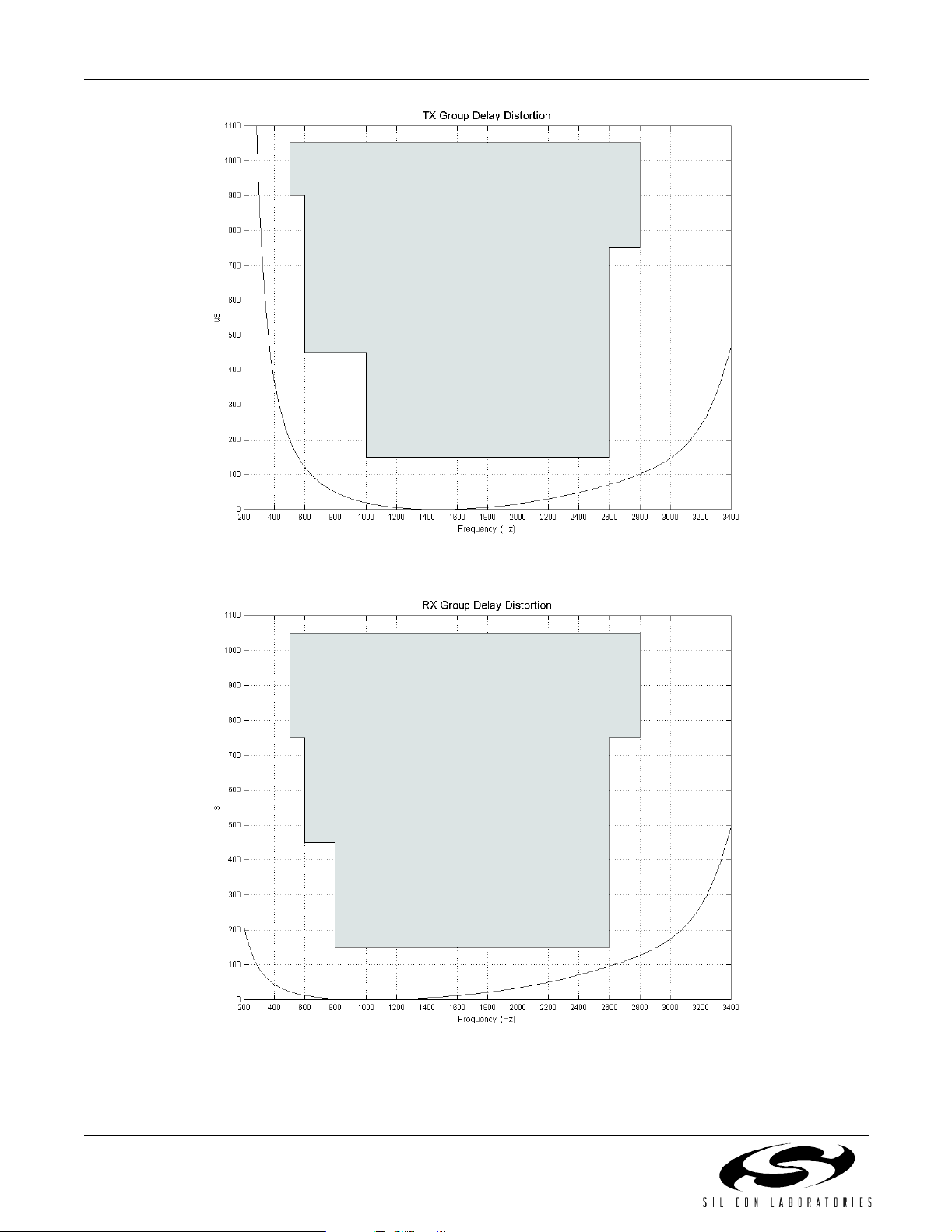
Group Delay Over Frequency Figure 5,6 — —
Gain Tracking
3
1014 Hz sine wave, refer-
ence level –10 dBm
signal level:
3 dB to –37 dB –0.25 — 0.25 dB
–37 dB to –50 dB –0.5 — 0. 5 dB
–50 dB to –60 dB –1.0 — 1. 0 dB
PK
Round-Trip Group Delay at 1000 Hz — 1100 — µs
Gain Step Accuracy –6 dB to 6 dB –0.017 — 0.017 dB
Gain Variation with Temperature All gain settings –0.25 — 0.25 dB
Gain Variation with Supply V
DDA
= V
3.3/5 V ± 5% –0.1 — 0.1 dB
DDA =
2-Wire Return Loss 2 00 Hz to 3.4 kHz 30 35 — dB
Transhybrid Balance 300 Hz to 3.4 kHz 30 — — dB
Noise Performance
Idle Channel Noise
4
C-Message Weighted — — 15 dBrnC
Psophometric Weighted — — –75 dBmP
3 kHz flat — — 18 dBrn
PSRR from VDDA RX and TX, DC to 3.4 kHz 40 — — dB
PSRR from VDDD RX and TX, DC to 3.4 kHz 40 — — dB
PSRR from VBAT RX and TX, DC to 3.4 kHz 40 — — dB
Preliminary Rev. 1.11 5
Page 6

Si3210/Si3211/Si3212
Table 3. AC Characteristics (Continued)
(V
, V
DDA
Paramete r Test Condi t ion Min Typ Max Unit
= 3.13 to 5.25 V, TA = 0 to 70°C for K-Grade, –40 to 85°C for B-Grade)
DDD
Longitudinal Performance
Longitudinal to Metallic or PCM
Balance
200 Hz to 3.4 kHz, β
150, 1% mismatch
β
= 60 to 240
Q1,Q2
β
= 300 to 800
Q1,Q2
Q1,Q2
5
5
≥
56 60 — dB
43 60 — dB
53 60 — dB
Metallic to Lon g it u din al Balanc e 200 Hz t o 3.4 k H z 40 — — dB
Longitudinal Impedance 200 Hz to 3.4 kHz at TIP or
RING
Register selectable
ETBO/ETBA
00
01
10
—
—
—
33
17
17
—
—
—
Ω
Ω
Ω
Longitudinal Current per Pin Active off-hook
200 Hz to 3.4 kHz
Register selectable
ETBO/ETBA
00
01
10
Notes:
1. The input signal level should be 0 dBm0 for frequencies greater than 100 Hz. For 100 Hz and below, the level should be
–10 dBm0. The output signal magnitude at any other frequency will be smaller than the maximum value specified.
2. Analog signal measured as V
3. The quantization errors inherent in the µ/A-law companding process can generate slightly worse gain tracking performance
in the signal range of 3 dB to –37 dB for signal frequencies that are integer divisors of the 8 kHz PCM sampling rate.
4. The level of any unwanted tones within the bandwidth of 0 to 4 kHz does not exceed –55 dBm.
5. Assumes normal distribution of betas.
TIP
– V
. Assumes ideal line impedance matching.
RING
—
—
—
4
8
8
—
—
—
mA
mA
mA
6 Preliminary Rev. 1.11
Page 7
Si3210/Si3211/Si3212
Figure 1. Transmit and Receive Path SNDR
9
8
7
6
Fundamental
Output Power
(dBm0)
5
4
3
2.6
2
1
123456789
0
Fundamental Input Power (dBm0)
Acceptable
Region
Figure 2. Overload Compression Performance
Preliminary Rev. 1.11 7
Page 8
Si3210/Si3211/Si3212
Typical Response
Typical R esponse
Figure 3. Transmit Path Frequency Response
8 Preliminary Rev. 1.11
Page 9
Si3210/Si3211/Si3212
Figure 4. Receive Path Frequency Response
Preliminary Rev. 1.11 9
Page 10
Si3210/Si3211/Si3212
Figure 5. Transmit Group Delay Distortion
Figure 6. Receive Group Delay Distortion
10 Preliminary Rev. 1.11
Page 11

Si3210/Si3211/Si3212
Table 4. Linefeed Characteristics
(V
, V
DDA
Parameter Symbol Test Condition Min Typ Max Unit
= 3.13 to 5.25 V, TA = 0 to 70°C for K-Grade, –40 to 85°C for B-Grade)
DDD
Loop Resistance Range R
LOOP
DC Loop Current Accuracy I
DC Open Circuit Voltage
Accuracy
DC Differential Output
R
DO
LIM
Active Mode; V
See note.* 0 — 16 0 Ω
= 29 mA, ETBA = 4 mA –10 — 10 %
= 48 V,
– V
< I
OC
RING
LIM
V
TIP
I
LOOP
Resistance
DC Open Circuit Voltage—
Ground Start
DC Output Resistance—
V
OCTO
R
ROTO
I
RING<ILIM
I
RING<ILIM
; V
V
OC
wrt ground
RING
= 48 V
; RING to ground — 160 — Ω
Ground Start
DC Output Resistance—
R
TOTO
TIP to ground 150 — — kΩ
Ground Start
Loop Closure/Ring Ground
I
= 11.43 mA –20 — 20 %
THR
Detect Threshold Accuracy
Ring Trip Threshold
R
= 11 00 Ω –20 — 20 %
THR
Accuracy
Ring Trip Response Time User Programmable Register 70
and Indir ect Register 36
Ring Amplitude V
Ring DC Offset R
TR
OS
5 REN load; sine wave;
R
LOOP
= 160 Ω, V
BAT
= –75 V
Programmable in Indirect
Register 19
–4 — 4 V
—160— Ω
–4 — 4 V
———
44 — — V
RMS
0——V
Trapezoidal Ring Crest
Crest factor = 1.3 – .05 — .05
Factor Accuracy
Sinusoidal Ring Crest
R
CF
1.35 — 1.45
Factor
Ringing Frequency Accuracy f = 20 Hz –1 — 1 %
Ringing Cadence Accuracy Accuracy of ON/OFF Times –50 — 50 msec
Calibration Time ↑CAL to ↓CAL Bit — — 600 msec
Power Alarm Threshold
At Power Threshold = 300 mW –25 — 25 %
Accuracy
*Note: DC resistance round trip; 160 Ω corresponds to 2 kft 26 gauge AWG.
Preliminary Rev. 1.11 11
Page 12

Si3210/Si3211/Si3212
Table 5. Monitor AD C Character i sti cs
(V
, V
DDA
Parameter Symbol Test Condition Min Typ Max Unit
= 3.13 to 5.25 V, TA = 0 to 70°C for K-Grade, –40 to 85°C for B-Grade)
DDD
Differential Nonlinearity
DNLE –1/2 — 1/2 LSB
(6-bit resolution)
Integral Nonlinearity
INLE –1 — 1 LSB
(6-bit resolution)
Gain Error (voltage) — — 10 %
Gain Error (current) — — 20 %
Table 6. Si321x DC Characteristics, V
(V
DDA,VDDD
= 4.75 V to 5.25 V, TA = 0 to 70°C for K-Grade, –40 to 85°C for B-Grade)
DDA
= V
DDD
= 5.0 V
Parameter S ymb ol Test Condition Min Typ Max Unit
High Level Input Voltage V
Low Level Input Volt age V
High Level Output Voltage V
Low Level Output Voltage V
IH
IL
DIO1,DIO2,SDITHRU:IO = –4 mA
OH
OL
SDO, DTX:I
DOUT: IO = –40 mA
DIO1,DIO2,DOUT,SDITHRU:
I
= 4 mA
O
SDO,INT
,DTX:IO = 8 mA
= –8 mA
O
0.7 V
DDD
— — 0.3 V
V
– 0.6 — — V
DDD
V
– 0.8 — — V
DDD
——0.4V
——V
DDD
V
Input Leakage Current I
L
Table 7. Si321x DC Characteristics, V
(V
DDA,VDDD
= 3.13 V to 3.47 V , TA = 0 to 70°C for K-Grade, –40 to 85°C for B-Grade)
DDA
= V
DDD
= 3.3 V
–10 — 10 µA
Parameter Symbol Test Condition Min Typ Max Unit
High Level Input Voltage V
Low Level Input Voltage V
High Level Output Voltage V
Low Level Output Voltage V
Input Leakage Current I
IH
IL
OH
OL
L
DIO1,DIO2,SDITHRU:IO = –2 mA
SDO, DTX:I
DOUT: IO = –40 mA
DIO1,DIO2,DOUT,SDITHRU:
SDO,INT
= –4 mA
O
I
= 2 mA
O
,DTX:IO = 4 mA
0.7 V
DDD
— — 0.3 V
V
– 0.6 — — V
DDD
V
– 0.8 — — V
DDD
——0.4V
–10 — 10 µA
—— V
DDD
V
12 Preliminary Rev. 1.11
Page 13

Table 8. Power Supply Characteristics
(V
DDA,VDDD
= 3.13 V to 5.25 V, TA = 0 to 70°C for K-Grade, –40 to 85°C for B-Grade)
Si3210/Si3211/Si3212
Parameter
Power Supply Current,
Analog and Digital
Power Supply Current, V
BAT
Symbol Test Condi t io n
+ I
I
A
D
Sleep (RESET = 0) 0.1 0.25 0.42 mA
Open 33 42.8 49 m A
Active on-hook
ETBO = 4 mA
Active OHT
ETBO = 4 mA 57 72 83 mA
Active off-hook
ETBA = 4 mA, I
Ground-start 36 47 55 mA
Ringing
Sinewave, REN = 1, V
3
I
BAT
Sleep (RESET = 0) — 0 — m A
Open (DCOF = 1) — 0 — mA
Active on-hook
= 48 V, ETBO = 4 mA — 3 —
V
OC
Active OHT
ETBO = 4 mA — 11 —
1
Typ
Typ
46 57 68 mA
= 20 mA 73 88 9 9
LIM
= 56 V 45 55 65
PK
2
Max Unit
mA
mA
mA
mA
Active off-hook
ETBA = 4 mA, I
= 20 mA — 30 —
LIM
mA
Ground-start — 2 — m A
Ringing
V
PK_RING
= 56 VPK,
—5.5—
mA
sinewave ringing, REN = 1
Notes:
1. V
2. V
3. I
, V
, V
DDA
DDA
= 3.3 V.
= 5.25 V.
(the large negative supply). For a switched-mode power supply regulator efficiency of 71%,
BAT
DDD
DDD
= current from V
BAT
the user can calculate the regulator current consumption as I
BAT
V
BAT
/(0.71 VDC).
Table 9. Switching Characteristics—General Inputs
V
= V
DDA
Parameter Symbol Min Typ Max Unit
Rise Time, RESET
RESET
Note: All timing (except Rise and Fall time) is referenced to the 50% level of the waveform. In put t est levels are VIH = VD –
= 3.13 to 5.25 V, TA = 0 to 70°C for K-Grade, –40 to 85°C for B-Grade, CL = 20 pF)
DDA
Pulse W i dt h t
0.4 V, V
= 0.4 V. Rise and Fall times are refer enced to the 20% and 80% levels of the waveform.
IL
t
r
rl
— — 20 ns
100 — — ns
Preliminary Rev. 1.11 13
Page 14
Si3210/Si3211/Si3212
Table 10. Switching Characteristics—SPI
V
DDA
= V
= 3.13 to 5.25 V, TA = 0 to 70°C for K-Grade, –40 to 85°C for B-Grade, CL = 20 pF
DDA
Parameter
Symbol
Cycle Time SCLK t
Rise Time, SCLK t
Fall Time, SCL K t
Delay Time, SCL K Fall to SDO Active t
Delay Time, SCL K Fall to SDO
Transition
Delay Time, CS
Setup Time, CS
Hold Time, CS
Rise to SDO Tri-state t
to SCLK Fall t
to SCLK Rise t
Setu p Time, SD I to SCL K Rise t
Hold Time, SDI to SCLK Rise t
Delay Time between Chip Selects t
SDI to SDITHRU Propagation Delay t
d1
t
d2
d3
su1
h1
su2
h2
cs
cs
Test
Conditions
c
r
f
Min Typ Max Unit
0.062 — — µsec
— — 25 ns
— — 25 ns
— — 20 ns
— — 20 ns
— — 20 ns
25 — — ns
20 — — ns
25 — — ns
20 — — ns
220 — — ns
—4—ns
Note: All timing is referenced to the 50% level of the waveform. Input test levels are V
t
t
r
thru
t
c
SCLK
t
su1
CS
t
t
su2
h2
SDI
t
d1
t
d2
SDO
Figure 7. SPI Timing Diagram
IH
= V
–0.4 V, VIL = 0.4 V
DDD
t
r
t
h1
t
cs
t
d3
14 Preliminary Rev. 1.11
Page 15
Si3210/Si3211/Si3212
Table 11. Switchi n g C h ar acteristic s—PCM H igh way Seri al I n ter face
VD = 3.13 to 5.25 V, TA = 0 to 70°C for K-Grade, –40 to 85°C for B-Grade, CL = 20 pF
Parameter
Symbol
PCLK Frequency 1/t
PCLK Duty Cycle Tolerance t
PCLK Period Jitter Tolerance t
jitter
Rise Time, PCLK t
Fall Time, PCL K t
Delay Time, PCLK Rise to DTX Active t
Delay Time, PCLK Rise to DTX
t
c
dty
r
f
d1
d2
Test
Conditions
Transition
Delay Time, PCLK Rise to DTX Tri-state
Setup Time, FSYNC to PCLK Fall t
Hold Time, FSYNC to PCLK Fall t
Setup Time, DRX to PCLK Fall t
Hold Time, DRX to PCLK Fall t
Notes:
1. All timing is ref erenced to the 50% level of the waveform. Input test levels are V
2. Spec applies to PCLK fall to DTX tri-state when th at mode is selected (TRI = 0).
2
t
d3
su1
h1
su2
h2
Min
—
—
—
—
—
—
—
—
1
Typ
0.256
0.512
0.768
1.024
1.536
2.048
4.096
8.192
1
Max
—
—
—
—
—
—
—
—
1
Units
MHz
MHz
MHz
MHz
MHz
MHz
MHz
MHz
40 50 60 %
–120 — 120 ns
— — 25 ns
— — 25 ns
— — 20 ns
— — 20 ns
— — 20 ns
25 — — ns
20 — — ns
25 — — ns
20 — — ns
IH – VI/O –
0.4V, VIL = 0.4V
PCLK
FSYNC
DRX
DTX
t
r
t
su1
t
c
t
h1
t
su2th2
t
d1
t
d2
Figure 8. PCM Highway Interface Timing Diagram
t
f
t
d3
Preliminary Rev. 1.11 15
Page 16
Si3210/Si3211/Si3212
0
F
220nF
Q4
5401
R10
10
C8
R13
5.1k
Q2
5401
R11
10
Q5
5551
C7
220nF
R7
80.6
C26
0.1uF
R21
15
Q9
2N2222
1
1
R28
R29
Note 1
Q1
5401
TIP
Protection
Circuit
22nF
22nF
Q6
5551
C5
C6
RING
Notes:
1. Values and configurations for these
components can be derived from Table 19
or from App Note 45.
2. Only one component per system needed.
3. All circuit grounds should have a singlepoint connection to the ground plane.
R6
80.6
GND
5401
GND
VCC
GND
3123102730
32
TEST
R1
200k
15
20
R8
C3
470
220nF
28
29
17
R2
200k
220nF
26
25
R4
200k
19
R5
200k
18
C4
R9
470
21
16
R3
200k
Q3
R12
5.1k
VCC
GNDD
STIPDC
STIPAC
ITIPP
ITIPN
STIPE
IRINGP
IRINGN
SRINGE
SVBAT
SRINGAC
SRINGDC
SDCL
SDCH
9
8
SDCL
SDCH
DC-DC Converter
VBAT VDC
Circuit
GNDA
Si3210/Si3210M
DCDRV
34
DCDRV
VDDD
VDDA2
VDDA1
DCFF
33
DCFF
SCLK
SDI
SDO
FSYNC
PCLK
DRX
DTX
INT
RESET
IGMP
IGMN
IREF
CAPP
CAPM
QGND
VDC
38
37
36
1
CS
6
3
4
5
2
7
24
22
11
12
14
13
VDDA1
C15
0.1uF
R15
243
C2
10uFC110uF
C16
0.1uF
SPI Bus
PCM Bus
VCC
2
R32
10k
Note 2
2
R26
40.2k
R14
40.2k
VDDA2 VDDD
C17
0.1uF
C3
10u
Figure 9. Si3210/Si3210M Typical Application Circuit Using Integrated DC-DC Converter
Table 12. Si3210/Si3210M External Component Values
Compon ent Value Suppl ier/Part Number
C1,C2 10 µF, 6 V Ceramic/Tantalum or 16 V Low Leakage Elec-
trolytic, ±20%
C3,C4 220 nF, 100 V, X7R, ±20% Murata, Johanson, Novacap, Venkel
C5,C6 22 nF, 100 V, X7R, ±20% Murata, Johanson, Novacap, Venkel
C7,C8 220 nF , 50 V, X7R, ±20% Murata, Johanson, Novacap, Venkel
C15,C16,C17 0.1 µF, 6 V, Y5V, ±20% Murata, Johanson, Novacap, Venkel
C26 0.1 µF, 100 V, X7R, ±20% Murata, Johanson, Novacap, Venkel
C30 10 µF, 16 V , Electrolytic, ±20% Panasonic
Q1,Q2,Q3,Q4 100 V, PNP, BJT Central Semi CMPT5 401; ON Semi
Q5,Q6 100 V, NPN, BJT Cent ral Semi CZT5551, ON Semi 2N5551
Q9 NPN General Purpose BJT ON Semi MMBT2222ALT1, MPS2222A; Cent ral
R1,R2,R3,R4,R5 200 kΩ, 1/10 W , ±1%
R6,R7 80.6 Ω, 1/4 W, ±1%
R8,R9 470 Ω, 1/10 W, ±1%
R10,R11 10 Ω, 1/10 W, ±5%
R12,R13 5.1 kΩ, 1/10 W, ±5%
R14,R26* 40.2 kΩ, 1/10 W, ±1%
R15 243 Ω, 1/ 1 0 W, ±1%
R21 15 Ω, 1/4 W, ±1%
R28,R29 1/10 W, ±1% (See AN45 or Table 17 for value selection)
R32* 10 kΩ, 1/10 W, ±5%
*Note: Only one component per system needed.
Murata, Panasonic, Nichicon URL16100MD,
Panasonic Z Series
MMBT5401LT1, 2N5401; Zetex FMMT5401
Semi CMPT2222A; Zetex FMMT2222
16 Preliminary Rev. 1.11
Page 17
Si3210/Si3211/Si3212
T
VDC
F1
SDCH
SDCL
Si3210
DCFF
DCDRV
Notes:
1. Values and configurations for these components can be derived
from Table 21 or from App Note 45.
2. Voltage rating for C14 and C25 must be greater than VDC.
C10
22nF
1
R19
Note 1
1
R20
R16
200
R18
Q8
2N2222
R17
Note 1
L1
1
Q8
FZT953
D1
ES1D
C25
10uF
2
GND
10uF
2
C14
0.1uF
VBA
C9
Figure 10. Si3210 BJT/Induc tor DC-DC Converter Circuit
T a ble 13. Si3210 BJT/Inductor DC-DC Converter Component Values
Component (s) Value Supplier
C9 10 µF, 100 V, Electrolytic, ±20% Panasonic
C10 22 nF, 50 V, X7R, ±20% Murata, Johanson, Novacap, Venkel
C14* 0.1 µF, X7R, ±20% Murata, Johanson, Novacap, V enkel
C25* 10µF, Electrolytic, ±20% Panasonic
R16 200 Ω, 1/10 W, ±5%
R17 1/10 W, ±5% (See AN45 or Table 19 for value selecti on)
R18 1/4 W, ±5% (See AN45 or Table 19 for value selection)
R19,R20 1/10 W, ±1% (See AN45 or Table 19 for value selection)
F1 Fuse Belfuse SSQ Series
D1 Ultra Fast Recovery 200V, 1A Rectifier General Semi ES1D; Central Semi
CMR1U-02
L1 1A, Shielded Inductor (See AN45
Table 19 for value selecti on)
Q7 120 V, High Current Switching PNP Zetex FZT95 3, FZT955, ZTX953,
Q8 60 V, General Purpose Swit ching NPN ON Semi MMBT2222ALT1, MPS2222A;
*Note: Voltage rating of thi s device must be greater than V
DC
or
.
API Delevan SPD127 series, Sumida
CDRH127 series, Datatro nics DR340-1
series, Coilcraft DS5022, TDK
SLF12565
ZTX955
Central Semi CMPT2222A; Zetex
FMMT2222
Preliminary Rev. 1.11 17
Page 18
Si3210/Si3211/Si3212
T
VDC
F1
SDCH
SDCL
C27
Si3210M
DCFF
DCDRV
Notes:
1. Values and configurations for these components can be derived
2. Voltage rating for C14 and C25 must be greater than VDC.
470pF
R17
200k
NC
from Table 20 or from App Note 45.
R19
Note 1
R20
M1
IRLL014N
R22
1
2
1
R18
1
22
Note 1
C25
10uF
1
2
D1
ES1D
3
6
4
10
1
T1
GND
C9
10uF
C14
0.1uF
2
VBA
Figure 11. Si3210M MOSFET/Transformer DC-DC Converter Circuit
Table 14. Si3210M MOSFET/Transformer DC-DC Converter Component Values
Component (s) Value Supplier
C9 10 µF, 100 V, El ec trolyt ic , ±20% Panas onic
C14* 0.1
C25* 10
C27 470 pF, 100 V, X7R, ±20% Murata, Johanson, Novacap, Venkel
R17 200 k
R18 1/4 W, ±5% (See AN45 or Table 18 for value selection)
R19,R20 1/10 W , ± 1% (See AN45 or Table 18
R22 22
F1 Fuse Belfuse SSQ Series
D1 Ultra Fast Recovery 200 V, 1A Rectifier General Semi ES1D; Central Sem i
T1 Power Transformer Coiltronic CTX01-15275;
M1 100 V, Logic Level Input MOSFET Intl Rect. IRLL014N; Intersil
*Note: V oltage rating of this device must be greater t han VDC.
µF, X7R, ±20% Murata, Johanson, Novacap, Venkel
µF, Electrolytic, ±20% Panasonic
Ω, 1/10 W, ± 5%
for value selection)
Ω, 1/10 W, ±5%
CMR1U-02
Datatronics SM76315;
Midcom 31353R-02
HUF76609D3S; ST Micro
STD5NE10L, STN2NE10L
18 Preliminary Rev. 1.11
Page 19
Q1
5401
TIP
Protection
Circuit
22nF
22nF
C5
C6
5551
Q6
R6
80.6
RING
Notes:
1. Only one component per system needed.
2. All circuit grounds should hav e a singl e-point
connection to the ground plane.
Figure 12. Si3211/12 Typical Application Circuit Using Extended Battery
C8
220nF
Si3210/Si3211/Si3212
VCC
3123102730
32
R1
C3
220nF
220nF
200k
R8
470
R2
200k
R4
200k
R5
200k
C4
R9
470
R3
200k
R18
1.8k
GND
Q4
5401
R10
10
R13
5.1k
C7
C9
R16
200k
Q3
5401
R11
10
R12
5.1k
GND
Q7
5401
VBATL
4003
Q2
5401
Q5
5551
220nF
R7
80.6
0.1uF
Q8
5551
D1
VBATH
15
STIPDC
20
STIPAC
28
ITIPP
29
ITIPN
17
STIPE
26
IRINGP
25
IRINGN
19
SRINGE
18
SVBAT
21
SRINGAC
16
SRINGDC
TEST
GNDA
GNDD
Si3211/Si3212
DIO2
DIO1
DCSW
9
8
34
NC NC NC
VDDD
VDDA2
VDDA1
DOUT
33
SCLK
SDI
SDO
FSYNC
PCLK
DRX
DTX
INT
RESET
IGMP
IGMN
IREF
CAPP
CAPM
QGND
CS
C15
0.1uF
38
37
36
1
6
3
4
5
2
7
24
R15
243
22
11
12
C2
14
13
C1
10uF
10uF
VDDA1 VDDA2 VDDD
C17
C16
0.1uF
0.1uF
SPI Bus
PCM Bus
VCC
1
R32
10k
Note 1
1
R26
40.2k
R14
40.2k
Table 15. Si3211/12 External Component Values
Component Value Supplier/Part Number
C1,C2 10 µF, 6 V Ceramic/Tantalum or 16 V Low
Leakage Electrolytic, ±20%
C3,C4 220 nF, 100 V, X7R, ±20% Murata, Johanson, Novacap, Venkel
C5,C6 22 nF , 100 V, X7R, ±20% Murata, Johanson, Novacap, Venkel
C7,C8 220 nF, 50 V, X7R, ±20% Murata, Johanson, Novacap, Venkel
C9 0.1 µF, 100 V, Electrolytic, ±20% Panasonic
C15,C16,C17 0.1 µF, 6 V, Y5V, ±20% Murata, Johanson, Novacap, Venkel
R1,R2,R3,R4,R5,R16 200 kΩ, 1/1 0 W, ±1%
R6,R7 80.6 Ω, 1/4 W, ±1%
R8,R9 470 Ω, 1/10 W, ±1%
R10,R11 10 Ω, 1/10 W, ±5%
R12,R13 5.1 kΩ, 1/10 W, ±5%
R14,R26* 40.2 kΩ, 1/10 W, ±1%
R15 243 Ω, 1/10 W, ±1%
R18 1.8 kΩ, 1/10 W, ±5%
R32* 10 kΩ, 1/10 W, ±5%
D1 200V 1A Rectifier ON Semi MRA4003, 1N4003
Q1,Q2,Q3,Q4,Q7 100 V, PNP, BJT Central Semi CMPT5401; ON Semi MMBT5401LT1,
Q5,Q6 100 V, NPN, BJT Central Semi CZT5551, ON Semi 2N5551
Q8 100 V, NPN, BJT Centr al Semi CMPT5551, ON Semi 2N5551
*Note: Only one component per system needed.
Murata, Panasonic, Nichicon URL16100MD, Pana-
sonic Z Seri es
2N5401; Zetex FMMT5401
Preliminary Rev. 1.11 19
Page 20
Si3210/Si3211/Si3212
RRE
80.6
QRDN
Q3
5401
R23
RRBN0
3.0k
RTE
80.6
QTN
Q6
5551
R6
QRP
Q5
5551
R12
R7
RRBN
5.1k
CRBN
100 nF
C7
R13
RTBN
5.1k
QTDN
Q4
5401
R24
RTBN0
3.0k
C8
CTBN
100 nF
Figure 13. Si321x Optional Equivalent Q5, Q6 Bias Circuit
Table 16. Si321x Optional Bias Component Values
Component Value Supplier/Part Number
C7,C8 100 nF, 100 V, X7R, ±20% Murata, Johanson, Venkel
R23,R24 3.0 kΩ, 1/10 W, ±5%
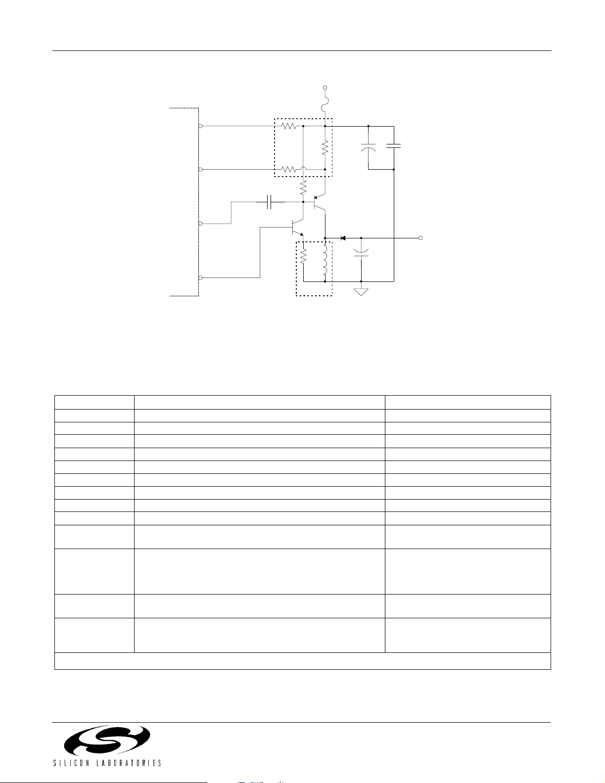
The subcircuit above can be substituted into any of the ProSLIC solutions as an optional bias circuit for Q5, Q6. For
this optional subcircuit, C7 and C8 are different in voltage and capacitance to the standard circuit. R23 and R24 are
additional components.
Table 17. Component Value Selection for Si3210/Si3210M
Component Val ue Comments
R28 1/10 W, 1% resistor
For V
For V
= 3.3 V: 26.1 kΩ
DD
= 5.0 V: 37.4 kΩ
DD
R29 1/10 W, 1% resistor
For V
For V
For V
= 80 V: 541 kΩ
CLAMP
= 85 V: 574 kΩ
CLAMP
= 100 V: 676 kΩ
CLAMP
where V
where V
R28 = (V
BE
R29 = V
CLAMP
+ VBE)/148 µA
DD
is the nominal VBE for Q9
/148 µA
CLAMP
is the cl amping voltage for V
BAT
Tab le 18. Compo nent Value Selection Examples for Si3210M MOSFET/Transformer DC-DC Converter
VDC Ringing Load/Loop Resistance Transformer Ratio R18 R19, R20
3.3 V 3 REN/117 Ω 1 - 2 0.56 Ω 7.15 kΩ
5.0 V 5 REN/117 Ω 1 - 2 0.10 Ω 16.5 kΩ
12 V 5 REN/1 17 Ω 1 - 3 0.68 Ω 56.2 kΩ
24 V 5 REN/1 17 Ω 1 - 4 2.20 Ω 121 kΩ
Note: There ar e other system and software condit ions that influen ce component value selection, so pl ease refer to
AN45 “Design Guide for the Si3210 DC -DC Conv er ter for detailed guidance.
Table 19. Component Value Selection Examples for Si3210 BJT/Inductor DC-DC Converter
VDC Ringing Load/Loop Length L1 R17 R18 R19, R20
5 V 3 REN/11 7 Ω 33 µH100Ω 0.12Ω 16.5 kΩ
12 V 5 REN/117Ω 150 µH162Ω 0.56Ω 56.2kΩ
24 V 5 REN/117Ω 560 µH274Ω 2.2 Ω 121 kΩ
Note: There are other s ystem and software conditions that influence component value selection, so
please refer to AN45 “Design Guide for the Si3210 DC-DC Converter for detailed guidance.
20 Preliminary Rev. 1.11
Page 21
Functional Description
t
Si3210/Si3211/Si3212
The ProSLIC™ is a single low-voltage CMOS device
that provides all the SLIC, codec, DTM F detection, and
signal generation functions needed for a complete
analog telephone interface. The ProSLIC performs all
battery, overvoltage, ringing, supervision, codec, hybrid,
and test (BORSCHT) function s. Unlike most monolithic
SLICs, the Si3210 does not require externally supplied
high-voltage battery supplies. Instead, it generates all
necessary battery voltages from a positive dc supply
using its own dc-dc converter controller. Two fully
programmable tone generators can produce DTMF
tones, phase continu ous FSK (caller ID) signaling, and
call progress tones. DTMF decoding and pulse metering
signal generation are also integrated.
The ProSLIC is ideal for short loop applications, such as
terminal adapters, cable telephony, PBX/key systems,
wireless local loop (WLL) , and voice over IP solutions.
The device meets all relevant LSSGR and CCITT
standards.
The linefeed provides programmable on-hook voltage,
programmable off-hook loop current, reverse battery
operation, loop or gro und start operation, and on-hook
transmission ringing voltage. Loop curr ent and voltage
are continuously monitored using an integrated A/D
converter. Balanced 5 REN ringing with or without a
programmable dc offset is integrated. The available
offset, frequency, w aveshape, and cadence options are
designed to ri ng the widest variety of terminal devices
and to reduce external controller re quirem ents.
A complete audio transmit and receive path is
integrated, including DTMF decoding, ac impedance,
and hybrid gain. These features are software
programmable, all owing for a single hardwar e design to
meet international requirements. Digital voice data
transfer occurs over a standard PCM bus. Cont rol data
is transferred using a standard SPI. The device is
available in a 38-pin TSSOP.
Linefeed Interface
The ProSLIC’s linefeed interface offers a rich set of
features and programmable flexibility to meet the
broadest applications requirements. The dc linefeed
characteristics are software program mable; key current,
voltage, and power measurements are acquired in
realtime and provided in software registers.
1.5 V steps. The loop current limit (I
) defines the
LIM
constant current zone and is programmable from 20 mA
to 41 mA i n 3 mA steps. The ProSLIC has an inherent
dc output resistance (R
V
(TIP-RING)
V
(V)
OC
) of 160 Ω.
O
Constant
Voltage
Zone
R
=160 Ω Constant Curren
O
I
LIM
Zone
I
LOOP
(mA )
Figure 14. Simplified DC Current/Voltage
Linefeed Characteristic
The TIP-to-R ING v oltage (VOC) is offset from ground by
a programmable voltage (V
) to provide voltage
CM
headroom to the posit ive-most terminal (TIP in forward
polarity states and RING in reverse polarity states) for
carrying audio signals. Table 20 summarizes the
parameters to be initialized before entering an active
state.
Table 20. Programmable Ranges of DC
Linefeed Character i stics
Parameter Programmable
I
LIM
V
OC
V
CM
*Note: The ProSLIC uses registers that are both directly
and indirectly mapped. A “direct” regist er is one that
is mapped directly.
Range
20 to 41 mA 20 mA ILIM[2:0] Direct
0 to 94.5 V 48 V VOC[5:0] Direct
0 to 94.5 V 3 V VCM[5:0] Direct
Default
Value
Register
Bits
Location*
Register 71
Register 72
Register 73
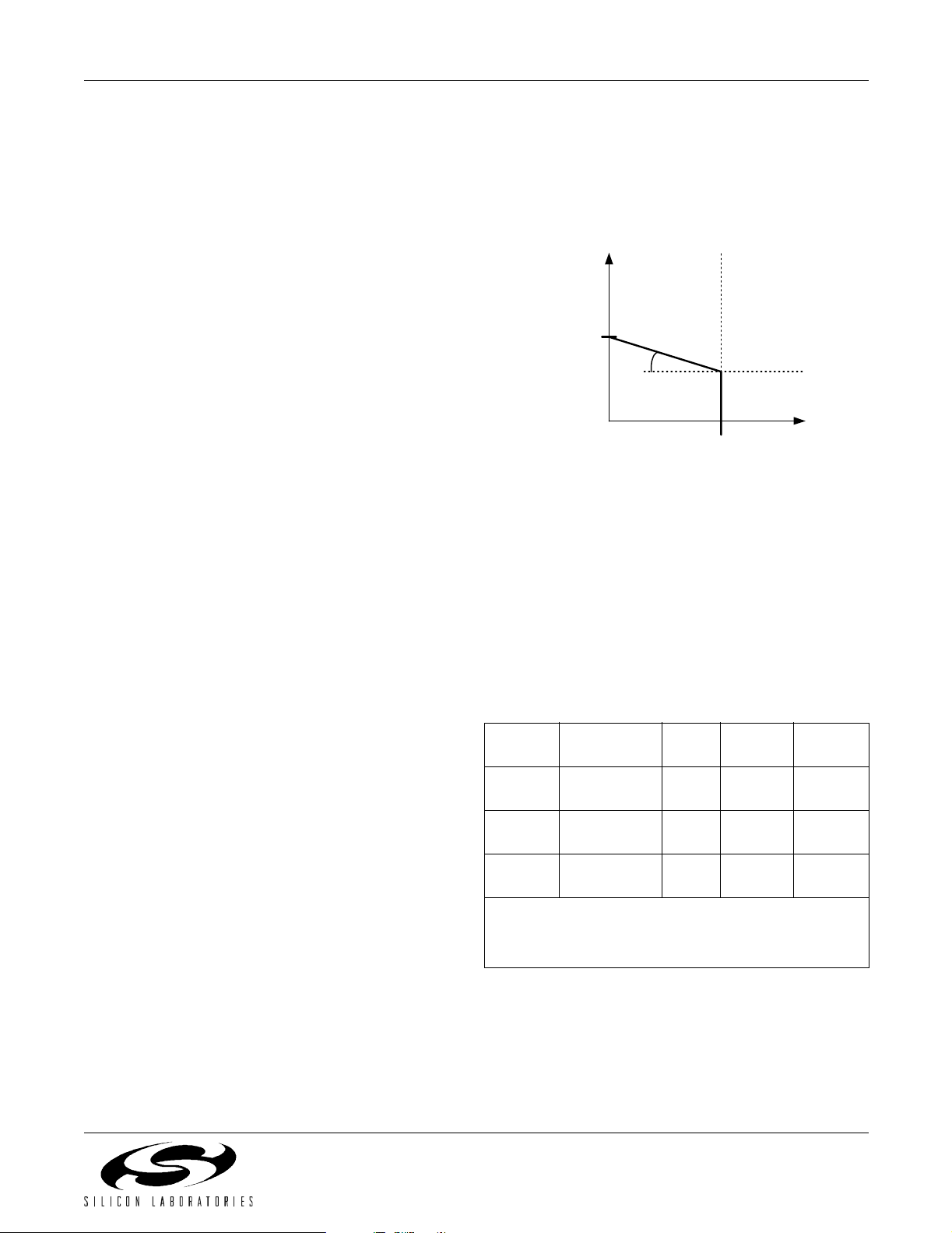
DC Feed Characteristics
The ProSLIC has pro grammable constant v oltage and
constant current zones as depicted in Fig ure 14. Open
circuit TIP-to-RING voltage (V
) defines the c onstant
OC
voltage zone and is programmable from 0 V to 94.5 V in
Preliminary Rev. 1.11 21
Page 22

Si3210/Si3211/Si3212
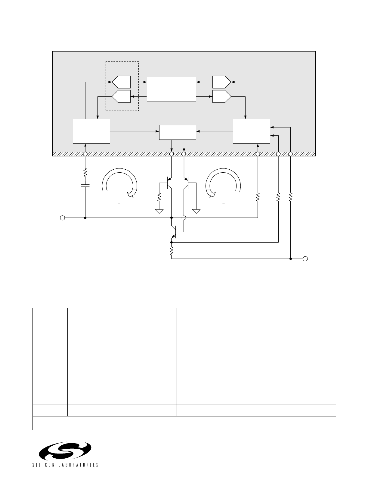
Linefeed Architecture
The ProSLIC is a low-voltage CMOS d evice that uses
low-cost external components to control the high
voltages required for subscriber line interfaces.
Figure 15 is a simplified illustration of the linefeed
control loop circuit for TIP or RING and the external
components used.
The ProSLIC uses both voltage and c urrent sensing to
control TIP and RING. DC and AC line voltage s on TIP
and RING are measured through sense resistors R
DC
and RAC, respectively. The ProSLIC uses linefeed
transistors Q
and QN to drive TIP and RING. Q
P
DN
isolates the high-voltage base of QN from the ProSLIC.
The ProSLIC measures voltage at various nodes in
order to monitor the linefeed current. R
provide access to these measuring points. The
R
BAT
, RSE, and
DC
sense circuitry is calibrated on-chip to guarantee
measurement accuracy with standard external
component tolerances. See "Linefeed Calibration" on
pa ge 26 for det ails.
Linefeed Operation States
The ProSLIC linefeed has eight states of operatio n as
shown in Table 21. The state of operation is controlled
using the Linefeed Control register ( direc t Regis ter 64).
The open state turns off all currents into the external
bipolar transistors and can be used in the presence of
fault conditions on the line and to generate Open Switch
Intervals (OSIs). TIP and RING a re effectivel y tri-stated
with a dc output impedance of about 150 k
Ω. The
ProSLIC can also automat ic ally ent er the open state if it
detects excessive power being consumed in the
external bipolar transist ors. See "Power Monitoring and
Line Fault Detection" on page 24 for more details.
In the forward active and reverse ac tive states, linef eed
circuitry is on and the audio s ignal paths are powered
down.
In the forward and revers e on-hoo k transmis sion s tates
audio signal paths are powered up to provide data
transmission during an on-hook loop condition.
The TIP Open state turns off all control cur rents to the
external bipolar devices connec ted to TIP and provides
an active linefeed on RING for ground start operation.
The RING Open state provides similar operation with
the RING drivers off and TIP active.
The ringing state drives programmable ringing
waveforms onto the line.
Loop Voltage and Current Monitoring
The ProSLIC continuo usly monitors the TIP and RING
voltages and external BJT currents. These values are
available in regis ters 78–89. Table 22 o n page 24 lis ts
the values that are measured and their associated
registers. An internal A/D converter samples the
measured voltages and currents from the analo g sense
circuitry and translates them into the digital domain. The
A/D updates the samples at an 800 Hz rate. Two
derived values are also reported—loop voltage and loop
current. The loop v olta ge, V
TIP–VRING
, is reported as a
1-bit sign, 6-bit magnitude format. For ground start
operation the reported value is t he RING voltage. The
loop current, (I
– IQ2 + IQ5 –IQ6)/2, is reported i n a 1-
Q1
bit sign, 6-bit magnit ude format. In RING op en and TIP
open states the loop cu rrent is report ed as (I
–IQ6).
(I
Q5
– IQ2) +
Q1
22 Preliminary Rev. 1.11
Page 23
Aud i o
Codec
Si3210/Si3211/Si3212
Monitor A/D
TIP or
RING
A/D
A/D
DSP
D/AD/A
SLIC DAC
AC
Control
R
C
AC
AC
AC Sense
AC
Control
Loop
R
BP
On-ChipExternal Components
Σ
Q
Q
DN
P
Q
N
R
E
DC
Control
Loop
DC
Control
DC Sense
R
DC
Battery Sense
Emitter Sense
R
SE
R
BAT
V
BAT
Figure 15. Simplified ProSLIC Linefeed Architecture for TIP and RING Leads (One Shown)
Table 21. ProSLIC Linefeed Operations
LF[2:0]* Linefeed State Description
000 Open TIP and RING tri-stated.
001 For ward Active V
010 Forward On-Hook Transmission V
011 TIP Open TIP tri-state d, RING active; used for ground s tart.
100 Ringing Ringing waveform applied to TIP and RING.
101 Reverse Active V
110 Reverse On-Hook Transmission V
1 11 Ring Open RING tri-stated, TIP active.
Note: The Linefeed register (LF) is locat ed in direct Register 64.
TIP
TIP
RING
RING
> V
> V
> V
> V
.
RING
; audio signal paths powered on.
RING
.
TIP
; audio signal paths powered on.
TIP
Preliminary Rev. 1.11 23
Page 24

Si3210/Si3211/Si3212
4096
P
h
Table 22. Measure d Re al ti me Linefe ed Interfa ce Charac ter i stics
Parameter Measurement
Loop Voltage Sense (V
TIP
– V
Range
) –94.5 to +94.5 V 1.5 V L V SP,
RING
Resolution Register
Bits
Location*
Direct Register 78
LVS[6:0]
Loop Current Sense –80 to +80 mA 1.27 mA LCSP,
Direct Register 79
LCS[5:0]
TIP Voltage Sense 0 to –95.88 V 0.376 V VTIP[7:0] Direct Register 80
RING Voltage Sense 0 to –95.88 V 0.376 V VRING[7:0] Direct Register 81
Battery Voltage Sense 1 (V
Battery Voltage Sense 2 (V
) 0 to –95.88 V 0.376 V VBATS1[7:0] Direct Register 82
BAT
) 0 to –95.88 V 0.376 V VBATS2[7:0] Direct Register 83
BAT
Transistor 1 Current Sense 0 to 81.35 mA 0. 319 m A IQ1[7: 0] Direct Register 84
Transistor 2 Current Sense 0 to 81.35 mA 0. 319 m A IQ2[7: 0] Direct Register 85
Transistor 3 Current Sense 0 to 9.59 mA 37.6
Transistor 4 Current Sense 0 to 9.59 mA 37.6
µA IQ3[7:0] Di r ect Regist er 86
µA IQ4[7:0] Di r ect Regist er 87
Transistor 5 Current Sense 0 to 80.58 mA 0. 316 m A IQ5[7: 0] Direct Register 88
Transistor 6 Current Sense 0 to 80.58 mA 0. 316 m A IQ6[7: 0] Direct Register 89
*Note: The ProSLIC uses registers that are both directly and i ndi rectly mapped. A “direct” regi ster is one that is mapped
directly.
Power Monitoring and Li ne Fa u lt D et ec ti on
In addition to reporting voltages and currents, the
ProSLIC continuously monit ors the power dissipated in
the type of fault condition present on the line .
The value of each thermal low-pass filter pole is set
according to the equation:
each external bipolar t ransistor. Realtime output power
of any one of the six linefeed transistors c an be read by
setting the Power Monitor Pointe r (direct Regis ter 76) to
point to the des ir ed t r ansis tor and then reading the Line
Power Output Monitor (direct Register 77).
The realtime power measurem ents are low- pass filter ed
and compared to a maximum power threshold.
Maximum power thresholds and filter time constants are
software programmable and should be set for each
transistor pair based on the characteristics of the
transistors used. Table 23 describes the registers
associated with this function. If the power in any
---------------- -
800 τ⋅
where
thermal LPF register
τ is the thermal time constant of the transistor
package, 4096 is the full range of the 12-bit register, and
800 is the sample rate in hertz. Ge ner ally
for SOT223 packages and
τ = 0.16 seconds f or SO T23,
but check with the manufacturer for the package
thermal con stant of a specif ic device. F or example, t he
power alarm threshol d and low-pass filt er values fo r Q5
and Q6 using a SOT223 package transistor are
computed as follows:
3
2
⋅=
τ = 3 seconds
external transisto r exceeds the programm ed threshold,
a power alarm event is tri ggered. The ProSLIC sets the
Power Alarm register bit, generates an interrupt (if
enabled), and automatically enters the Open state (if
AOPN = 1). This feature protects the external
transistors from fault con ditions and , com bined wit h the
loop voltage and current m onitors, allows diagnosis of
MAX
PPT56
-------------------------------
====
Resolution
Thus, indirect Register 34 should be set to 150Dh.
Note: The power monitor resolution for Q3 and Q4 is differen t
from that of Q1, Q2, Q5, and Q6.
7
1.28
------------------
2
⋅
0.0304
7
2
⋅ 5389 150D
24 Preliminary Rev. 1.11
Page 25

Si3210/Si3211/Si3212
Table 23. Associated Power Monitoring and Power Fault Registers
Parameter Description/
Range
Power Monit o r Po i nter 0 to 5 points to Q 1
to Q6, respe ctively
Line Power Monitor Output 0 to 7.8 W for Q1,
Q2, Q5, Q6
0 to 0.9 W for Q3,
Q4
Power Alarm Threshold, Q1 & Q2 0 to 7.8 W 30.4 mW PPT12[7:0] Indirect Register 32
Power Alarm Threshold, Q3 & Q4 0 to 0.9 W 3.62 mW PPT34[7:0] Indirect Register 33
Power Alarm Threshold, Q5 & Q6 0 to 7.8 W 30.4 mW PPT56[7:0] Indirect Register 34
Thermal LPF Pole, Q1 & Q2 see equation above NQ12[7:0] Indirect Register 37
Thermal LPF Pole, Q3 & Q4 see equation above NQ34[7:0] Indirect Register 38
Thermal LPF Pole, Q5 & Q6 see equation above NQ56[7:0] Indirect Register 39
Power Alarm Interrupt Pending Bits 2 to 7 corre-
spond to Q1 to Q6,
respectively
Resolution Register
Bits
n/a PW RM P[2: 0] Direct Register 76
30.4 mW
3.62 mW
n/a QnAP[n+1],
PWROM[7:0] Direct Regis t er 77
where n =1
to 6
Location*
Direct Register 19
Power Alarm Interrupt Enable Bits 2 to 7 corre-
spond to Q1 to Q6,
respectively
Power Alarm
Automatic/Manual Detect
*Note: The ProSLIC uses registers that are both directly and i ndi rectly mapped. A “direct” regi ster is one that is mapped
directly. An “indirect” register i s one that is accessed using the indirect access regist ers (direct registe rs 28 th rough
31).
0 = manual mode
1 = enter open state
upon power alarm
n/a QnAE[n+1],
where n = 1
to 6
n/a A OP N Direct Register 67
Direct Register 22
Preliminary Rev. 1.11 25
Page 26
Si3210/Si3211/Si3212
LCS
LVS
Input
Signal
Processor
LCVELFS
ISP_ OU T
Digital
LPF
NCLR
HYSTEN
Loop Closure
Threshold
LCRTLLCRT
Figure 16. Loop Closure Detection
Loop Closure Detection
A loop closure event signals that the terminal equipment
has gone off-hook durin g on-hook transmission or onhook active states. The ProSLIC perform s loop closure
detection digitally using its on-chip monitor A/D
converter. The functional bloc ks required to implement
loop closure detection are shown in Figure 16. The
primary input to the system is the Loop Current S ense
value provided in the LCS register (direct Register 79).
The LCS value is processed in the Input Signal
Processor when the ProSLIC is in the on-hook
transmission or on-hook active linefeed state, as
indicated by the Linefeed Shadow register, LFS[2:0]
(direct Register 64). The data then feeds into a
programmable digital low-pass filter, which removes
unwanted ac signal components before threshold
detection.
The output of the low-pass filter is compared to a
programmable threshold, LCRT (indirect register 28).
The threshold comparator output feeds a programmable
debouncing filter. The output of the debouncing filter
remains in its pres ent state unles s the input remains in
the opposite state for the entire period of time
programmed by the loop closure debounce interval,
LCDI (direct Regist er 69). I f the debounce interval has
been satisfied, th e LCR bit will be se t to indicate that a
valid loop closure has oc c urr ed. A loop closure interru pt
is generated if enabled by the LCIE bit (direct
Register 22). Table 24 lists the registers that must be
written or monitored to correctly detect a loop closure
condition.
Loop Closu r e Threshold H y st ere sis
Silicon revisions C and higher support the addition of
programmable hyste resis to the loop closu re threshold,
which can be enabled by setting HYSTEN = 1 (direct
Register 108, b it 0). The hyst eresis is defined b y LCRT
(indirect Register 28) and LCRTL (indirect Regi ster 43),
+
Debo un ce
Filter
–
LCDI
LCR
Interrupt
Logic
LCIE
LCIP
which set the upper and lower bounds, res pec tive ly.
Voltage-Based Loop Closure Detection
Silicon revisions C and highe r also support an optional
voltage-based loop closure detection mode, which is
enabled by setting LCVE = 1 (direct Register 108,
bit 2). In this mode t he loop voltage is co mpared to the
loop closure threshold register (LCRT) which represents
a minimum voltage threshold instead of a maximum
current threshold. If hysteresis is also enabled, then
LCRT represents the upper voltage boundary and
LCRTL represents the lower voltage boundary for
hysteresis. Although voltage-based loop closure
detection is an option, the default current-based loop
closure detection is recommended.
Table 24. Register Set for Loop
Closure Detection
Parameter R egi ster Location
Loop Closure
Interrupt Pending
Loop Closure
Interrupt Enable
Loop Closure Threshold LCRT[5:0] Indir ect Reg. 28
Loop Closure
Threshold—Lower
Loop Closure Filter
Coefficient
Loop Closure Detect
Status (monitor only)
Loop Closure Detect
Debounce Interval
Hysteresis Enable HYSTEN Direct Reg. 108
Voltage-Based Loop
Closure
Linefeed Calibra t i on
LCIP Direct Reg. 19
LCIE Direct Reg. 22
LCRTL[5:0] Indirect Reg. 43
NCLR[12:0] Indirect Reg. 35
LCR Direct Reg. 68
LCDI[6:0] Direct Reg. 69
LCVE Direct Reg. 108
26 Preliminary Rev. 1.11
Page 27

Si3210/Si3211/Si3212
An internal calibration algorithm corrects for internal and
external component errors. The calibration is initiated by
setting the CAL bit in direct Register 96. Upon
completion of the calibration cycle, this bit is
automatically reset.
It is recommended that a calibration be executed
following system power-up. Upon release of the chip
reset, the Si3210 will be in the open state. After
powering up the dc-dc converter and allowing it to settle
for time (t
) the calibration can be initiated.
settle
Additional calibrations may be performed, but only one
calibration should be necessary as long as t he system
remains powered up.
During calibration, V
BAT
, and V
TIP
voltages are
RING
, V
controlled by the calibration engine to provide the
correct external voltage conditions for the algorithm.
Calibration should be performed in the on-hook state.
RING or TIP must not be connected to ground during
the calibration.
Battery Voltage Generation and Switching
The ProSLIC supports two modes of battery supply
operation. First, the Si3210 integrates a dc-dc converter
controller that dynamically regulates a single output
voltage. This mode eliminates t he need to suppl y large
external battery voltages. Instead, it converts a single
positive input voltage into the real-t ime battery voltage
needed for any given state according to programmed
linefeed parameters. Second, the Si3211 and Si3212
support switching between high and low battery voltage
supplies, as would a traditional monolithic SLIC.
For single to low channel count applications, the Si3210
proves to be an economical choice, as the dc-dc
converter eliminate s the need to design and build highvoltage power supplies. For higher channel count
applications whe re cent ralized batt ery voltag e supp ly is
economical, or for modular legacy systems where
battery voltage is already available, the Si3211 and
Si3212 are recommended.
DC-DC Converter General Description
(Si3210/Si3210M Only)
The dc-dc converter dynamically generates the large
negative voltages required to operate the linefeed
interface. The Si3210 ac ts as the controller for a buckboost dc-dc converter that converts a positive dc
voltage into the desired negative battery voltage. In
addition to eliminating external power supplies, this
allows the Si3210 to dynamically control the battery
voltage to the minimum r equired for any given mode of
operation.
Two different dc-dc circuit options are offered: a BJT/
inductor version and a MOSFET/transformer version.
Due to the differences on the drivi ng circuits, there are
two different versions of the Si3210. The Si3210
supports the BJT/inductor circuit option, and the
Si3210M version supports the MOSFET solution. The
only difference bet ween the two versions is the polarity
of the DCFF pin with respect to the DCDRV pin. For the
Si3210, DCDRV and DCFF are opposite polarity. For
the Si3210M, DCDRV and DCFF are the sam e polarity.
Table 25 summarizes these differences.
Table 25. Si3210 and Si3210M Differences
Device DCFF Signal
Polarity
Si3210
= DCDRV
Si3210M = DCDRV 1
Notes:
1.
DCFF signal polarity wit h respect to DCDRV signal.
2. Di rect Register 93, bit 5; This is a read-only bit.
Extensive design guidance on each of these circuits can
be obtained from Application Note 45 (AN45) and from
an interactive dc-dc converter design spreadsheet. Both
of these documents are available on the Silicon
Laboratories website (www.silabs.com).
BJT/Inductor Circuit Option Using Si3210
The BJT/Inductor circuit option, as defined in Figure 9,
offers a flexible, low-cost solution. Depending on
selected L1 inductance value and the switching
frequency, the input voltage (V
) can range from 5 V to
DC
30 V. By nature of a dc-dc converter ’s operation, peak
and average input currents can become large with small
input voltages. Consider this when selecting the
appropriate i nput voltage and pow er rating for the V
power supply.
For this solution, a PNP power BJT (Q7) switch es the
current flow through low E SR inductor L1. The Si3210
uses the DCD RV and DCFF pins to switch Q7 o n and
off. DCDRV controls Q7 t hrough NPN BJT Q8. DCFF is
ac coupled to Q7 through capacitor C10 to assist R16 in
turning off Q7. Therefore, DCFF must have opposite
polarity to DCDRV, and the Si321 0 (not Si321 0M) must
be used.
MOSFET/Transformer Circuit Option Using Si3210M
The MOSFET/transformer circuit option, as defined in
Figure 11, offers higher power efficiencies across a
larger input voltage range. Depending on the
transformers primary inductor value and the switching
frequency, the input voltage (V
) can range from 3.3 V
DC
to 35 V. Therefore, it is possible to power the entire
ProSLIC solution from a single 3.3 V or 5 V power
supply. By nature of a dc-dc converter’s operation, peak
DCPOL
0
DC
Preliminary Rev. 1.11 27
Page 28

Si3210/Si3211/Si3212
and average input currents can become large with small
input voltages. Consider this when selecting the
appropriate input voltage and power rating for the V
DC
power supply (number of REN supported).
For this solution, an n-channel power MOSFET (M1)
switches the cur rent flow through a p ower transformer
T1. T1 is specified in Applicat ion Note 45 (AN45), and
includes several taps on the prim ary side to facilitate a
wide range of input voltages. The Si3210M version of
the Si3210 must be used for the application circuit
depicted in Figure 9 because the DCFF pin is used to
drive M1 directly and therefore must be the same
polarity as DCDRV. DCDRV is not used in this circuit
option; connecting DCFF and DCDRV together is not
recommended.
DC-DC Converter Architecture
(Si3210/Si3210M Only)
The control logic for a pulse width modulated (PWM) dcdc converter is incor porated in the S i3210. O utput pins ,
DCDRV and DCFF, are used to switch a bipolar
transistor or MOSFET. The polarity of DCFF is opposite
to that of DCDRV.
The dc-dc converter circuit is powered on when the
DCOF bit in the Power Down Register (direct
Register 14, bit 4) is cleared to 0.
The switching
regulator circuit within the Si3210 is a high
performance, pulse-width modulation controller. The
control pins are driven by the PWM controller logic in
the Si3210. The regulated output voltage (V
BA T
) is
sensed by the SVBAT pin and is used to detect whether
the output voltage is above or below an internal
reference for the desired battery voltage. The dc
monitor pins SDCH and SDCL monitor input current and
voltage to the dc-dc converter external circuitry. If an
overload condition is detected, the PWM controller w ill
turn off the sw itching transistor for the remainder of a
PWM period to prevent damage to external
components. It is important that the proper val ue of R18
be selected to ensure safe operation. Guidance is given
in Application Note 45 (AN45).
The PWM co ntroller o perates at a frequency se t by t he
dc-dc Converter PWM register (direct Register 92).
During a PWM period the outputs of the control pins
DCDRV and DCFF are asserted for a time given by the
read-only PWM Pulse Width register (direct
Register 94).
The dc-dc converter must be off for some time in each
cycle to allow the inductor or trans former to trans fer its
stored energy to the output capacitor, C9. This minimum
off time can be set through the dc-dc Converter
Switching Delay register, (direct Register 93). The
number of 16.384 MHz clock cycles that the controller is
off is equal to DCTOF (bits 0 throug h 4) plus 4. I f the dc
Monitor pins detect an overload condition, the dc-dc
converter interru pts its conversion cycles regardl ess of
the register settings to prevent component damage.
These inputs should be calibrated by writing the DCCAL
bit (bit 7) of the dc-dc Converter Switching Delay
register, direct Register 93, after the dc-dc converter
has been turned on.
Because the Si3210 dynamically regulates its own
battery supply voltage using the dc-dc converter
controller, the battery vo ltage (V
) is offset from the
BAT
negative-most terminal by a programmable voltage
) to allow voltage headroom for carrying audio
(V
OV
signals.
As mentioned previously, the Si3210 dynamically
adjusts V
illus tra te th i s, the be h av ior of V
to suit the particular circuit requirement. To
BAT
in the active state is
BAT
shown in Figure 17. In the active state, the TIP-t o- RING
open circuit voltage is kept at V
voltage region while the regulator output voltage, V
+ VOC + VOV.
V
CM
When the loop cu rrent attempts to exceed I
in the constant
OC
, the dc
LIM
BAT
=
line driver c ircuit ent ers cons tant current mode a llowing
the TIP to RING voltage to track R
. As the TIP
LOOP
terminal is kept at a constant voltage, it is the RING
terminal voltag e that tracks R
| voltage will als o track R
|V
BAT
R
= I
LIM
the VOC/I
continue to track R
+ VCM +VOV. As R
LOOP
mark, the regulator output voltage can
LIM
(TRACK = 1), or the R
LOOP
tracking mechanism is stopped when |V
and, as a result, the
LOOP
. In this state, |V
LOOP
decreases below
LOOP
BAT
| = |V
BAT
LOOP
BATL
(TRACK = 0). The former case is the more common
application and provides the maximum power
dissipation savings. In principle, the regulator output
voltage can go as low as |V
|=VCM+ VOV, offeri ng
BAT
significant powe r savings.
When TRACK = 0, |V
. The RING t erminal voltage, howev er, continues
V
BATL
to decrease with decreasing R
| will not decrease below
BAT
. The power
LOOP
dissipation on the NPN bipolar transistor driving the
RING terminal can become large and may require a
higher power rat ing device. The non-trac king mode of
operation is required by specific terminal equipment
which, in order to initiate certain data transmission
modes, goes briefly on-hook to measure the line voltage
to determine whether there is any other off-hook
terminal equipmen t on the same line. TRACK = 0 mode
is desired since the regulator output voltage has long
settling time constants (on the order of tens of
milliseconds) and cannot change ra pidly for TRACK = 1
mode. Therefore, the brief on-hook voltage
measurement would yield approximately the same
voltage as the off-hook line voltage and would cause the
terminal equipment to incorrectly sense another offhook terminal.
|
|
28 Preliminary Rev. 1.11
Page 29
V
V
V
BATL
T
R
A
C
TRACK=0
Si3210/Si3211/Si3212
OC
I
Constant I Re gi on Consta nt V Region
K
=
1
V
OV
LIM
|V
TIP
V
CM
- V
RING
|
V
OV
R
LOOP
V
TIP
V
OC
V
RING
V
BAT
Figure 17. V
TIP
, V
RING
, and V
in the For ward Acti ve State
BAT
Table 26. Associated Relevant DC-DC Converter Registers
Parameter Range Resolution Register Bit Location
DC-DC Converter Power-off
Control
DC-DC Converter Calibration
Enable/Status
DC-DC Converter PWM Period 0 to 15.564 us 61.035 ns DCN[7:0] Direct Register 92
DC-DC Converter Min. Off Time (0 to 1.892 us ) +
High Battery Voltage—V
Low Battery Voltage—V
V
OV
Note: The ProSLIC uses registers that are both directly and i ndi rectly mapped. A “direct” regi ster is one that is mapped
directly. An “indirect” register is one that i s accessed using the indirect access registers (direct r egisters 28 thr ough 31).
BATH
BATL
n/a n/a DCOF Direct Regist er 14
n/a n/a DCCAL Direct Register 93
61.035 ns DCTOF[4:0] Direct Register 93
4ns
0 to –94.5 V 1.5 V VBATH[5:0] Direct Reg i s ter 74
0 to –94.5 V 1.5 V VBATL[5:0] Direct Regist er 75
0 to –9 V or
0 to –13.5 V
1.5 V VMIND[ 3:0 ]
VOV
Indirect Register 41
Direct Register 66
Preliminary Rev. 1.11 29
Page 30

Si3210/Si3211/Si3212
DC-DC Converter Enhancements
Silicon revisions C and higher support two
enhancements to the dc-dc converter. The first is a
multi-threshold er ror control algorithm tha t enables the
dc-dc converter to adjust more quickly to voltage
changes. This option is enabled by setting DCSU = 1
(direct Register 108, bit 5). The se cond enhancement is
an audio band filter that removes audio band noise from
the dc-dc co nverter contro l loop. This o ption i s ena bled
by setting DCFIL = 1 (direct Register 108, bit 1).
DC-DC Converter During Ringing
When the ProSLIC enters the ringing state, it requires
voltages well above those used in the acti ve mo de. The
voltage to be generated and regulated by the dc-dc
converter during a ringin g burst is set us ing the VBATH
register (direct Register 74). VBATH can be set between
0 and –94.5 V in 1.5 V steps. To avoid clipping the
ringing signal, V
amplitude. At the end of each ringing burst the dc-dc
converter adjusts back to active state regulation as
described above.
External Battery Switching (Si3211 and Si3212 Only)
The Si3211 and Si3212 support switching between two
battery voltages. The circuit for external battery
switching is defined in Figure 12. Typically a high
voltage battery (e.g., –70 V) is used for on-hook and
ringing states, and a low v oltage battery (e.g., –24 V) is
used for the off-hook condition. The ProSLIC uses an
external transistor to switch bet ween th e two s upplies.
When the ProSLIC changes operating states, it
automatically sw it c hes bat t er y s upplies if the au tom at ic /
manual control bit ABAT (direct Register 67, bit 3) is set.
For example, the ProSLI C will switch from high batte ry
to low battery when it detects an off-hook ev ent t hr ough
either a ring trip or loop closure event. If automatic
battery selection is disabled (ABAT = 0), the battery is
selected by the Batt ery Feed Select bit, BATSL (direct
Register 66, bit 1).
Silicon revisions C and higher support the option to add
a 60 ms debounce period to the battery switching circuit
when transitioning from high batt ery to low batte ry. This
option is enabled by setting SWDB = 1 (direct
Register 108, bit 3). This debounce minimizes battery
transitions in the case of pulse dialing or other quick onhook to off-hook transitions.
must be set larger than the ringing
BATH
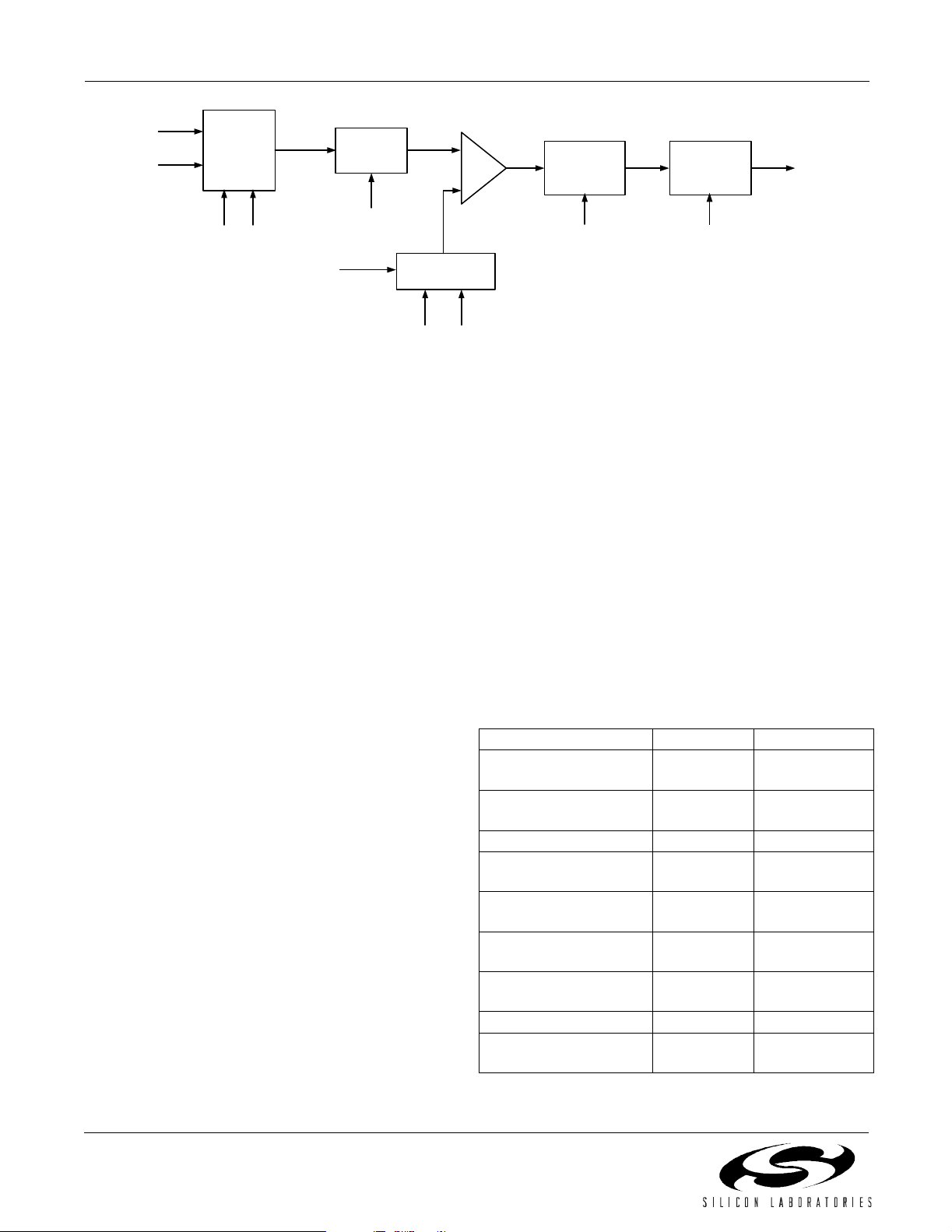
Tone Generation
Two digital tone generators are provided in the ProSLIC.
They allow the gener ation of a wide variety of single or
dual tone frequency and amplitude combinations and
spare the user the effort of generating the required
POTS signaling tones on the PCM highway. DTMF, FSK
(caller ID), call progress, and other tones can all be
generated on -chip. The tones can be sent t o either t he
receive or transmit paths (see Figure 23 on page 40).
Tone Generator Architecture
A simplified dia gram of the tone gener ator architecture
is shown in Figure 18. The oscillator, active/inactive
timers, interrupt block, and signal routing block are
connected to give the user flexibility in creating audio
signals. Control and status register bits are placed in the
figure to indicate their association with the tone
generator architect ur e. These r egisters are described in
more detail in Table 27.
30 Preliminary Rev. 1.11
Page 31

Si3210/Si3211/Si3212
Desired V
RMS
2π852
8000
15
1.78434
8 kHz
Clock
OnE
16-Bit
Modulo
Counter
OATn
OITn
*Tone Generator 1 Only
n = "1" or "2" for Tone Generator 1 and 2, respectively
OATnE
OITnE
OAT
Expire
OIT
Expire
Zero
Cross
Logic
INT
Logic
INT
Logic
OZn
Zero Cross
OSSn
Load
Logic
OnIP
OnIE
OnAP
OnAE
REL*
Enable
Register
Load
Figure 18. Simplified Tone Generator Diagram
Oscillator Frequency and Amplitude
Each of the two tone generators contains a two-pole
resonate oscillator circuit with a programmable
frequency and amplitude, which are programmed via
indirect registers OSC1, OSC1X, OSC1Y, OSC2,
OSC2X, and OSC2Y. The sample rate for the two
oscillators is 8000 Hz. The equations are as follows:
= cos( 2π fn/8000 Hz),
coeff
n
where f
where desired Vrms is the amplitude to be generated;
n = 1 or 2 for oscillator 1 or oscillator 2, respect iv ely.
For example, in order to generate a DTMF digit of 8, the
two required tones are 852 Hz and 1336 Hz. Assum ing
the generation of half-scale values (ignoring twist) is
desired, the following values are calculated:
is the frequency to be generated;
n
OSCn = coeff
1
1 coeff–
OSCnX
-- -
⋅⋅⋅=
4
------------------------
1 coeff+
OSCnY = 0,
coeff
OSC1 0.78434 2
OSC1X
1
1
0.21556
-- -
--------------------- 2
4
---------------- -
cos 0.78434==
()25701 6465h===
15
OSC1Y = 0
(215);
n
2151–()
----------------------------------------
1.11 V
1–()0.5 1424 590h==⋅⋅⋅=
RMS
8 kHz
Clock
Two-Pole
Resonanc e
Oscilla to r
OSCn
OSCnX
OSCnY
OSC2 = 0.49819 (2
OSC2X
coeff
1
---
4
Signal
Routing
OnSO
2π1336
--------------------
cos 0.49819==
2
0.50181
--------------------- 2
1.49819
8000
15
) = 16324 = 3FC4h
15
1–()0.5 2370 942 h==⋅⋅⋅=
to T X P ath
to RX P ath
OSC2Y = 0
The computed values above would be written to the
corresponding registers to initialize the oscillators. Once
the oscillators are initialized, the oscillator control
registers can be access ed to e nable th e oscill ators a nd
direct their outputs.
Tone Generator Cad ence P rog ra m m i ng
Each of the two tone generators contains two timers,
one for setting the a ctive per iod an d on e for setting the
inactive period. The oscillator signal is generated during
the active period and suspended during the inactive
period. Both the active and inactive periods can be
programmed from 0 to 8 seconds in 125
µs steps. The
active period time interval is set using OAT1 (direct
registers 36 and 37) for tone generator 1 and OAT2
(direct registers 40 and 41) for tone gener at or 2.
To enable automatic cadence for tone generator 1,
define the OAT1 and OIT1 registers and then set the
O1TAE bit (direct Register 32, bit 4) and O1TIE bit
(direct Register 32, bit 3). This enables each of the
timers to cont rol the state of the Oscillat or Enable bit,
O1E (direct Register 32, bit 2). The 16-bit counter will
begin counting until the active timer expires, at which
Preliminary Rev. 1.11 31
Page 32

Si3210/Si3211/Si3212
time the 16-bit counter will reset to zero and begin
counting until the inactive timer expires. The cadence
continues until the user clears the O1TAE and O1TIE
control bits. The zero crossing detect feature can be
implemented by setting the OZ1 bit (direct Register 3 2,
bit 5). This ensures that each oscillator pulse ends
without a dc component. The timing diagram in
Figure 19 is an exampl e of an ou tput cadenc e us ing the
zero crossing feature.
One-shot oscillation can be achiev ed by enabling O1E
and O1TAE. Direct control over the cadence can be
achieved by controlling th e O1E bit (direct Register 32,
bit 2) directly if O1TAE and O1TIE are disabled.
The operation of tone generat or 2 is id entical to that of
tone generator 1 using its respective control registers.
Note: Tone Generator 2 should not be enabled simulta-
neously with the ringing os cillat or due to res ource shar ing within the hardware.
Continuous phase frequency-shift keying (FSK)
waveforms may be creat ed using tone generato r 1 (not
available on tone generator 2) by setting the REL bit
(direct Register 32, bit 6), which enables reloading of
the OSC1, OSC1X, and OSC1Y registers at the
expiration of the active timer (OAT1).
Table 27. Associa ted Tone Gener ator Reg i sters
Tone Generator 1
Parameter Description / Range Register Bits Location
Oscillator 1 Frequency Coefficie nt Sets oscillator frequency OSC 1[1 5:0 ] Indirect Register 13
Oscillator 1 Amplit ude Coefficient Sets oscillator amplitude OSC1X[15:0] Indirect Register 14
Oscillator 1 initi al phase co efficie nt Se ts initia l phase OSC1Y[15:0] In dir ec t Regi ster 15
Oscillator 1 Active Timer 0 to 8 sec OAT1[15:0] Direct Registers 36 & 37
Oscillator 1 Inactive Timer 0 to 8 sec OIT1[15:0] Direct Register 38 & 39
Oscillator 1 Control Status and control
registers
Tone Generator 2
Parameter Description / Range Register Location
Oscillator 2 Frequency Coefficie nt Sets oscillator frequency OSC 2[1 5:0 ] Indirect Register 16
Oscillator 2 Amplit ude Coefficient Sets oscillator amplitude OSC2X[15:0] Indirect Register 17
Oscillator 2 initi al phase co efficie nt Se ts initia l phase OSC2Y[15:0] In dir ec t Regi ster 18
Oscillator 2 Active Timer 0 to 8 sec OAT2[15:0] Direct Registers 40 & 41
Oscillator 2 Inactive Timer 0 to 8 sec OIT2[15:0] Direct Register 42 & 43
Oscillator 2 Control Status and control
registers
OSS1, REL, OZ1,
O1TAE, O1TIE,
O1E, O1SO[1:0]
OSS2, OZ2,
O2TAE, O2TIE,
O2E, O2SO[1:0]
Direct Register 32
Direct Register 33
32 Preliminary Rev. 1.11
Page 33

Si3210/Si3211/Si3212
..
..
O1E
0,1 ...
OSS1
Tone
Gen. 1
Signal
Output
Figure 19. Tone Generator Timing Diagram
Enhanced FSK Waveform Generation
Silicon revisions C and higher support enha nced FSK
generation capabilities, which can be enabled by setting
FSKEN = 1 (direct Register108, bit 6) and REN = 1
(direct Register 32, bit 6). In this mode, the user can
define mark (1) and space (0) attributes once during
initialization by defining indirect registers 99–104. The
user need only indicate 0-to-1 and 1-to-0 transitions in
the information stream. By writing to FSKDAT (direct
Register 52) , this mod e applies a 24 kHz s am ple r at e to
tone generator 1 to give addit ional resolution to timers
and frequency generation. Application Note 32 gives
detailed instructions on how to implement FSK in this
mode. Additionally, sample source code is available
from Silicon Laboratories upon request.
Tone Generato r Inter rupts
Both the active and inactive timers can generat e their
own interrupt to signal “on/off” transitions to the
software. The timer interru pts for tone generator 1 can
be individually ena bled by setting the O1A E and O1IE
bits (direct Register 21, bits 0 and 1, respectively).
Timer interrupts for tone generator two are O2AE and
O2IE (direct Register 21, bits 2 and 3, respect ively). A
pending interrupt for each of the timers is determined by
reading the O1AP, O1IP, O2AP, and O2IP bits in the
Interrupt Status 1 register (direct Register 18, bits 0
through 3, respectively) .
0,1 ......, OAT1 ..., O A T1..., OIT10,1 ... 0,1 ...
.
.
ringing cadence. Both sinusoidal and trapezoidal ringing
waveforms are supported, and the trapezoidal crest
factor is programmable. Ringing signals of up to 88 V
peak or more can be gene rated, enabling the Pr oSLIC
to drive a 5 REN (1380
loop lengths of 2000 f eet (160
Ringing A rchitecture
The ringing generator architecture is nearly identical to
that of the tone generator. The sinusoid ringing
waveform is generated using an internal two-pole
resonance oscillator circuit with programmable
frequency and amplitude. However, since ringing
frequencies are very low compared to the audio band
signaling frequencies, the ringing waveform is
generated at a 1 kHz rate instead of 8 kHz.
The ringing generator has two timers that function t he
same as for the tone generator timers. They allow on/off
cadence settings up to 8 sec on/ 8 sec off. In addition to
controlling ringing cadence, these timers control the
transition into and out of the ringing state. Table 28
summarizes the list of registers used for ringing
generation.
Note: Tone generator 2 should not be enabled concurrently
with the ringing generator due to resource sharing
within the hardware.
Ω + 40 µF) ringe r load across
Ω) or more.
Ringing Generation
The ProSLIC provides fully programmable internal
balanced ringing with or without a dc offset to ring a
wide variety of terminal devices. All parameters
associated with ringing are software programmable:
ringing frequency, waveform, amplitude, dc offset, and
Preliminary Rev. 1.11 33
Page 34

Si3210/Si3211/Si3212
15
R
Desired VPK0to94.5V
--- -
RNGY 0=
2π20
1
70
RNGY 0=
Table 28. Registers for Ringing Generation
Parameter Range/ Desc riptio n Register
Location
Bits
Ringing Waveform Sine/Trapezoid TSWS Direct Register 34
Ringing Voltage Offset Enable Enabled/
RVO Direc t Regi ster 34
Disabled
Ringing Active Timer Enable Enabled/
RTA E Direct Register 34
Disabled
Ringing Inactive Timer Enable Enabled/
RTIE Dir ec t Regi ster 34
Disabled
Ringing Oscillator Enable Enabled/
ROE Direc t Regi ster 34
Disabled
Ringing Oscillator A ctiv e Timer 0 to 8 sec RAT[15:0] Direct Registers 48 and
49
Ringing Oscillator Ina ctiv e Timer 0 to 8 sec RIT[15: 0] Direc t Registers 50 and
51
Linefeed Control (Initiates Ringing State) Ringing State = 100b LF[2:0] Direct Register 64
High Battery Voltage 0 to –94.5 V VBATH[5:0] Direc t Regi ster 74
Ringing dc voltage offset 0 to 94.5 V ROFF[15:0] Indirect Regi ster 19
Ringing frequency 15 to 100 Hz R CO[ 15:0 ] Indir ec t Regi ster 20
Ringing amplitude 0 to 94.5 V RNGX[15:0] In dir ec t Regi ster 21
Ringing initial phas e Sets initial phase for
RNGY[15:0] Indirect Register 22
sinewave and period
for
trapezoid
Common Mode Bias Adjust During Ringing 0 to 22.5 V VCM R [3:0] Indirect Register 40
Note: The ProSLIC uses registers that are both directly and indirectly mapped. A “direct” regist er is one that is mapped
directly. An “indirect” regist er is one that is accessed using the indirect access regi sters (direct registers 28 through
31).
When the ringing state is invoked by writing
and f = desired ringing frequency in hertz.
LF[2:0] = 100 (direct Register 64), the ProSLIC will go
into the ringing state and start the first ring. At the
expiration of RAT, the ProSLIC will turn off the rin ging
NGX
waveform and will go to the on- hook transmission stat e.
At the expiration of RIT, ringing will again be initiated.
This process will continue as long as the two timers are
enabled and the Linefeed Contr ol register is set to the
ringing state.
Sinusoid a l Ri ngi ng
In selecti ng a ringing amp litude, the peak T IP-to-RING
ringing voltage must be greater than the selected on-
hook line voltage set ting (VOC, direct Regi ster 72). F or
example, to generate a 70 V
equations are as follows:
To configure the ProSLIC for sinusoidal ringing, the
frequency and amplitude are initializ ed by writing to the
following indirect registers: RCO, RNGX, and RNGY.
The equations for RCO, RNGX, RNGY are as follows:
RCO coeff 2
where
coeff
34 Preliminary Rev. 1.11
cos=
()⋅=
πf
2
-----------------------
1000 Hz
RNGX
1
1 coeff–
-- -
⋅⋅⋅=
------------------------
4
1coeff+
coeff
RCO 0.99211 2
---
4
()⋅ 32509 7E FDh===
0.00789
--------------------- 2
1.99211
15
--------------------------------------------------------------------
2
20 Hz ringing signal, the
PK
⋅
-----------------------
1000 Hz
15
15
------
96
96 V
0.99211=cos=
376 0177h==⋅⋅⋅=
()
Page 35

Si3210/Si3211/Si3212
Desired V
3
1
V
96
V
N
In addition, the user must select the sinusoi dal ringing
waveform by writing TSWS = 0 (direct Register 34,
bit 0).
Trapezoidal Ringing
RNGX 71 V
()
For a crest factor of 1.3 and a period of 0.05 sec
(20 Hz), the rise time requirement is 0.0153 sec.
PK
71
------
96
21524235 5EA Bh==⋅=
In addition to the sinusoidal ringing waveform, the
ProSLIC supports trapezoidal ringing. Figure 20
illustrates a trapezoidal ringing waveform with offset
.
V
ROFF
RCO 20 Hz, 1.3 cre st fact or()
2 24235⋅
------------------------------------
0.0153 8000⋅
396 018Ch===
In addition, the user mu st select the trapezoid al ringing
V
TIP-RING
waveform by writing TSWS = 1 in direc t Regist er 34.
Ringing DC voltage Offset
A dc offset can be added to the ac ringing waveform by
defining the offset voltage in ROFF (indirect
V
ROFF
T=1/freq
t
RISE
time
Register 19). The offset, V
signal when RVO is set to 1 (direct Regis ter 34, bit 1).
The value of ROFF is calculated as follo ws :
ROFF
, is added t o the ringi ng
ROFF
ROFF
----------------- -
15
2
⋅=
Linefeed Considerations During Ringing
Care must be taken to keep the generated ringing signal
Figure 20. Trapezoidal Ringing Waveform
within the ringing voltage rails (GNDA and V
BAT
) to
maintains proper biasing of the external bipolar
To configure the ProSLIC for trapezoidal ringing, the
user should foll ow the same basic procedure as in t he
Sinusoidal Ringing section, but using the following
equations:
1
RNGY
RNGX
-- -
Period 8000⋅⋅=
2
-----------------------------------
PK
96 V
15
2
()⋅=
transistors. If the ringing signal nears the rails, a
distorted ringing s ignal and excessive power dissipation
in the external transistors will result.
To preven t this invalid operation, set the VBATH val ue
(direct Register 74) t o a value hig her than the maximum
peak ringing vol tage. The discu ssion below outlines t he
considerations and eq uations that govern the selection
of the VBATH setting for a particular desired peak
ringing voltage.
First, the requ ired amount of ri nging overhead voltage,
, is calculated based on the maximum value of
⋅
2 RNGX
RCO
-------------------------------
=
t
RISE
8000⋅
RCO is a value which is added or subtrac ted from the
waveform to ramp the signal up or down in a linear
fashion. This value is a function of rise time, period, and
amplitude, where rise time and period are related
through the fol lowing equation for the crest factor of a
trapezoidal waveform.
t
RISE
-- -
=
4
-----------
T1
–
CF
2
where T = ringing period, and CF = desired crest factor.
For example, to generate a 71 V
, 20 Hz ringing
PK
signal, the equations are as follows:
1
1
-- -
RNGY 20 Hz()
2
----------------
20 Hz
8000 200 C8h==⋅⋅=
V
OVR
current through t he l oad, I
LOAD,PK
, the minimum current
gain of Q5 and Q6, and a reasonab le voltage required
to keep Q5 and Q6 out of satur ati on. For ringing s ignals
up to V
=87V, V
PK
However, to determine V
= 7.5 V is a safe value.
OVR
for a specific ca se, use the
OVR
equations below.
I
LOAD,PK
AC,PK
-------------------
R
LOAD
I
+ V
OS
AC,PK
REN
------------------
6.9 kΩ
I
+⋅==
OS
where:
N
is the ringing REN load (max value = 5),
REN
I
is the offset cur rent flowing in the lin e driver circuit
OS
(max value = 2 mA), and
= amplitude of the ac ringing waveform.
V
AC,PK
It is good practice to provide a buffer of a few more
milliamperes for I
LOAD,PK
to account for possible line
Preliminary Rev. 1.11 35
Page 36

Si3210/Si3211/Si3212
RPTP
leakages, etc. The total I
LOAD,PK
current should be
smaller than 80 mA.
β 1+
------------ -
β
80.6 Ω 1V+⋅⋅=
where
V
OVRILOAD,PK
β
is the minimum expected current gain of
transistors Q5 and Q6.
The minimum value for VBATH is therefore given by the
following:
VBATH V
++=
AC,PKVROFFVOVR
The ProSLIC is designed to create a fully balanced
ringing waveform, meaning that the TIP and RING
common mode voltage , (V
TIP
+ V
)/2, is fix ed. This
RING
voltage is referred to as VCM_RING and is
automatically set to the following:
VCM_RI NG
VBATH VCMR
----------------------------------------------
=
–
2
VCMR is an indirect register which provides the
headroom by the r inging waveform with respect to t he
VBATH rail. The value i s set as a 4-b it set ti ng in indirect
Register 40 with an LSB voltage of 1.5 V/LSB.
Register 40 shou ld be set with the calculated V
OVR
to
provide voltage headroom during ringing.
Silicon revisions C and higher support the option to
briefly increase the maximum differential current limit
between the voltage transition of TIP and RING from
ringing to a dc linefeed s tate. This mode is enabled by
setting ILIMEN = 1 (direct Regi ster 108, bit 7).
Ring Trip Detection
A ring trip event signals that the termi nal equipment has
gone off-hook during the ringing state. The ProSLIC
performs ring trip detection digitally using its on-chip
monitor A/D converter. The functional blocks required to
implement ring t r ip det ec t ion is s hown in Figure 21. The
primary input to the system is the Loop Current Sense
value provided by the current monitoring circuitry and
reported in direct Register 79. LCS data is processed by
the input signal proc essor when the ProSLIC is in the
ringing state as indicated by the Linefeed Shadow
register (direct Reg ister 64). The data then feeds into a
programmable digital low pass filter, which removes
unwanted ac signal components before threshold
detection.
LCS ISP_OUT
Input
Signal
Processor
LFS
Digital
LPF
NRTP
+
–
Ring Trip
Threshold
Figure 21. Ring Trip Detector
The output of the low pass filter is compared to a
programmable threshold, RPTP (indirect Register 29).
The threshold comparator output feeds a programmable
debouncing filter. The output of the debouncing filter
remains in its pres ent state unles s the input remains in
the opposite state for the entire period of time
programmed by the ring trip debounce interval,
RTDI[6:0] (direct Register 70). If the debounc e int erval
has been satisf ied, the RTP bit of dir ect Register 68 will
be set to indicate that a vali d ring trip has occurred. A
ring trip interrupt is generated if enabled by the RTIE bit
(direct Register 22). Table 29 lists the registers that
must be writt en or monitored to co rrectly detect a ring
DBIRAW
Debounc e
Filter
RTDI
RTP
Interrupt
Logic
RTIE
RTIP
trip condition.
The recommended val ues for RPTP, NRTP, and RTDI
vary according to the programmed ringing frequency.
Register values for various ringing frequencies are
given in Table 30.
36 Preliminary Rev. 1.11
Page 37

Si3210/Si3211/Si3212
2πf
Desired V
Table 29. Associated Registers for Ring Trip Detection
Parameter Register Location
Ring Trip Interrupt Pending RTIP Direct Regi ster 19
Ring Trip Interrupt Enable RTIE Direct Register 22
Ring Trip Detect Debounce Interval RTDI[6:0] D irec t Regi ster 70
Ring Trip Threshold RPTP[5:0] Indirec t Regist er 29
Ring Trip Filter Coefficient NRTP[12:0] Indirect Register 36
Ring Trip Detect Status (monitor only) RTP Direct Register 68
Note: The ProSLIC uses registers that are both directly and indirectly mapped. A “direct” regist er is one that is mapped
directly. An “indirect” regist er i s one that is accessed using th e indi rect access regist ers (direct registers 28 through
31).
T a ble 30. Recommended Ring Trip Values for Ringing
Ringing
NRTP RPTP RTDI
Frequency
Hz decimal hex decimal hex decimal hex
16.667 64 0200 34 mA 3600 15.4 ms 0F
20 100 0320 34 mA 3600 12.3 ms 0B
30 112 0380 34 mA 3600 8.96 ms 09
40 128 0400 34 mA 3600 7.5 ms 07
50 213 06A8 34 mA 3600 5 ms 05
60 256 0800 34 mA 3600 4.8 ms 05
Pulse Metering Generation
There is an additional tone generator suitable for
generating tones above the audio frequency. This
oscillator is provided for the generation of billing tones
which are typically 12 kHz or 16 kHz. The generator
follows the same algorithm as described in "Tone
Generation" on page 30 with the exception that the
sample rate for computation is 64 kHz instead of 8 kHz.
The equations are as follows:
PLSX
where full scale V
The initial phase of the pulse met ering sign al is set to 0
internally so there is no register to ser ve this pur pos e.
The pulse metering generator timers and associated
pulse metering t imer registers are s imilar to that of t he
tone generators. These timers count 8 kHz sample
1
1coeff–
-- -
------------------------
4
1 c oeff+
RMS
2151–()
⋅⋅=
= 0.85 V
----------------------------------------------
Full Scale V
for a matched load.
RMS
periods like the oth er tones even t hough the sinu soid is
coeff
--------------------------
cos=
64000 Hz
generated at 64 kHz.
RMS
RMS
PLSCO coeff 2151–()⋅=
Preliminary Rev. 1.11 37
Page 38

Si3210/Si3211/Si3212
Table 31. Associated Pulse Metering Generator Registers
Parameter Description / Range Register Bit s Location
Pulse Metering Frequency
Coefficient
Pulse Metering Amplitude
Coefficient
Pulse Meteri ng A tt ack/Decay
Ramp Rate
Pulse Metering Active Timer 0 to 8 sec PAT[15:0] Direct Registers 44 & 45
Pulse Metering Inactive Timer 0 to 8 sec PI T[ 15:0 ] Direct Register 46 & 47
Pulse Metering Control Status and control registers PSTAT, PMAE,
Note: The ProSLIC uses registers that are both directly and indirectly mapped. A “direct” regist er is one that is mapped
directly. An “indirect” regist er i s one that is accessed using th e indi rect access regist ers (direct registers 28
through 31).
The pulse metering oscillator has a volume envelope
(linear ramp) on the on/off transitions of the oscillator.
The volume value is incremented by the value in the
PLSD register (indirect Register 23) at an 8 kHz rate.
The sinusoidal generator output is multiplied by this
volume before bein g sent to the DAC. The volume w ill
ramp from 0 to 7FFF in increments of PLSD so the
value of PLSD will set the slope of the r amp. Wh en t he
pulse metering signa l is turned off, the volume will ramp
to 0 by decrementing according to the value of PLSD.
Pulse Metering Oscillator
Volume
8 Khz
Clip to 7FFF or 0
Figure 22. Pulse Metering Volume Envelope
Sets oscillator frequency PLSCO[15:0] Indir ec t Reg ister 25
Sets oscillator amplitude PLSX[15:0] Indirect Register 24
0 to PLSX (full amplitude) PLSD[15:0] Indir ect Register 23
Direct Register 35
PMIE, PMOE
DTMF Detection
The dual-tone multi-frequency (DTMF) tone signaling
standard is als o known as touch tone. It is a n in-band
signaling system used to replace the pulse-dial
signaling standard. In DTMF, two tones are used to
generate a DTMF digit. O ne tone is chosen from f our
possible row tones, and one tone is chosen from four
possible column tones. The sum of these tones
constitutes one of 16 possible DTMF digi ts.
DTMF Detection Architecture
DTMF detection i s per fo rmed us ing a modified Goer t ze l
algorithm to comput e the dual frequenc y tone (DFT) f or
each of the eight DTMF frequencies as well as their
X
+/–
To DAC
PLSD
second harmonics . At the end of the DFT com putation,
the squared magnitudes of t he DFT results for t he eight
DTMF fundamental tones are computed. The row
results are sorted to determine the strongest row
frequency; the column frequencies are sorted as well.
At the completio n of this process, a number of checks
are made to det ermine whether the strongest row a nd
column tones constitute a DTMF digit.
The detection process is performed twice within the
45 ms minim um tone time. A di git must be detected on
two consecutive tests following a pause to be
recognized as a new digit. If all tests pass, an int errupt
is generated, and the DTMF digit value is loaded into
the DTMF register. If tones are occurring at the
maximum rate of 1 00 ms per digit, the i nte rrupt must be
serviced within 85 ms so that the current digit is not
38 Preliminary Rev. 1.11
Page 39

overwritten by a new one. There is no bu ffering of the
digit information.
Audio Path
Unlike traditional SLICs, the codec function is integrated
into the ProSLIC. The 16-bit codec offers programmable
gain/attenuation blocks and several loop-back modes.
The signal path block diagram is shown in Figure 23.
Transmit Path
In the transmit path, the analog signal fed by the
external ac coupling capacitors is amplified by the
analog transmit amplifier, ATX, prior to the A/D
converter. The gain of the ATX is user selectable to one
of mute/–3.5/0/3.5 dB options. The main role of ATX is
to coarsely adjust the signal swing to be as close as
possible to the f ull-scale input o f the A/D co nverter in
order to maximize the signal-to-noise ratio of the
transmit path. After passing through an anti-aliasing
filter, the analog signal is processed by the A/D
converter, producing an 8 kHz, 16-bit wide, linear PCM
data stream. The standard requirements for transmit
path attenuation for signals above 3.4 kHz are
implemented as part of the c ombined decimation filter
characteristic of the A/D converter. One more digital
filter is available in the transmit path: THPF. THPF
implements the high-pass attenuation requ irements for
signals below 65 Hz. The linear PCM data stream
output from THPF is amplified by the transmit-path
programmable gain amplifier, ADCG, which can be
programmed from –
can receive the linear PCM da ta stream at this point to
perform the digit extraction when e nabled by the user.
The final step in the transmit path signal processing is
the user selectable A-law or
can reduce the data stream word width to 8 bits.
Depending on the PCM _Mode register selec tion, every
8-bit com p r es s e d s e rial data w or d w ill occupy one time
slot on the PCM highway, or every 16-bit
uncompressed serial data word will occupy two time
slots on the PCM highway.
∞ dB to 6 dB. The DTMF decoder
µ-law compression which
Si3210/Si3211/Si3212
Preliminary Rev. 1.11 39
Page 40

40 Preliminary Rev. 1.11
Si3210/Si3211/Si3212
TIP
RING
Off Chip On Chip
I
G
buf
m
From Billing Tone
RAC
DAC
XAC
HYBP
H
Transmit Path
ATX
DLM
Decimation
Filter
Digital
Loopback
+
–
H
A/D
Analog
Loopback
ALM1
THPF
Dual Tone
Generator
ADCG
DTMF
Decoder
Mute
TXM
+
µ/A-law
Compressor
Full
Analog
Loopback
Serial
Output
ALM2
Digital
TX
HYBA
–
+
From Billing
Tone DAC
ARX
D/A
Interpolation
Filter
RHPF
DACG
Mute
+
RXM
µ/A-law
Expander
Serial
Input
Digital
RX
Figure 23. AC Signal Path Block Diagram
Page 41

Si3210/Si3211/Si3212
Receive Path
In the receive path, the optionally compressed 8-bit data
is first expanded to 16-bit words. The PCM F regist er bi t
can bypass the expansion process, in which case two
8-bit words are assembled into one 16-bit word. DACG
is the receive path programmab le gain amplifier which
can be programmed from –
bit signal is then provided to a D/A converter. The
resulting analog signal is amplified by the analog
receive amplifier, ARX, which is user selectable to one
of mute/–3.5/0/3.5 dB options. It is then applied at the
input of the transconductance amplifier (Gm) which
drives the off-chip current buffer (I
Audio Characteristics
The dominant source of distortion and noise i n both the
transmit and receive paths is the quantization noise
introduced by the
process. Figure 1 on page 7 specifies the minimum
signal-to-noise-and-distortion ratio for either path for a
sine wave input of 200 Hz to 3400 Hz.
Both the
audio codec to transfer and process audio signals larger
than 0 dBm0 without clipping. The max imum PCM c ode
is generated for a
3.17 dBm0 or an A-law encoded sine wave of
3.14 dBm0. The ProSLIC overload clipping limits are
driven by the PCM encoding process. Figure 2 on page
7 shows the acceptable limits for the anal og-to-analog
fundamental power transfer-function, which bounds the
behavior of ProSLIC.
The transmit path gain distortion versus frequency is
shown in Figure 3 on page 8. The same figure also
presents the minimum required attenuation for any outof-band analog signal that may be appli ed on the line.
Note the presence of a high-pass filter transfer-function,
which ensures at least 30 dB of attenuation for signals
below 65 Hz. The low-pass filter transfer function which
attenuates signals above 3.4 kHz has to exceed the
requirements specified by the e quations in Figure 3 on
page 8 and it is implemented as part of the A-to-D
converter.
The receive path transfer function requirement, shown
in Figure 4 on page 9, is very similar to the transmit path
transfer function. The most notable difference is the
absence of the high-pass filter portion. Th e only other
differences are the maximum 2 dB attenuation at
200 Hz (as oppos ed to 3 dB for t he transmit path) and
the 28 dB of attenuation for any frequency above
4.6 kHz. The PCM data rate is 8 kHz and thus, no
frequencies greater than 4 kHz can be digitally encoded
in the data stream. From this point of view, at
frequencies greater than 4 kHz, the plot in Figure 4
µ-law and the A-law speech encoding allow the
∞ dB to 6 dB. An 8 kHz, 16-
).
BUF
µ-law or the A-law compression
µ-law encoded sine wave of
should be interpreted as the maximum allowable
magnitude of any spurious signals that are generated
when a PCM data stream representing a sine wave
signal in the range of 300 Hz to 3.4 kHz at a level of
0 dBm0 is applied at the digital input.
The group delay dist ortion in either path is limited to no
more than the levels indicated in Figure 5 on page 10.
The reference in Figure 5 is the smallest group delay for
a sine wave in the range of 500 Hz to 2500 Hz at
0dBm0.
The block d iagram f or t he voice-band sign al p roce ssing
paths are shown in F igure 23. Both the rec eive and the
transmit paths employ the optimal combination of
analog and digital signal processing to provide the
maximum performance while, at the sa me time, offering
sufficient flexibility to allow users to optimize for their
particular application of the ProSLIC. All programmable
signal-processing blocks are symbolically indicated in
Figure 23 by a dashed arrow across them. The two-wire
(TIP/RING) voice-band interface to the ProSLIC is
implemented using a small number of external
components. The receive path interface consists of a
unity-gain current buffer, I
interface is simply an ac coupling capacitor. Signal
paths, although implemented differentially, are shown
as single-ended for simplicity.
Transhybrid Balance
The ProSLIC provides programmable transhybrid
balance with gain block H. (See Figure 2 3.) In the ideal
case where the synthesized SLIC impeda nce matches
exactly the subscriber loop impedance, the transhybrid
balance should be set to subtract a –6 dB level from the
transmit path signal. The transhybrid balance gain can
be adjusted from –2.77 dB to +4.08 dB a round t he idea l
setting of –6 dB by programming the HYBA[2:0] bits of
the Hybrid Control register (direct Register 11). Note
that adjusting any of the analog or digital gain blocks will
not require any modi fication of the transhybrid balanc e
gain block, as the transhybrid gain is subtracted from
the transmit path signal prior to any gain adjustment
stages. The transhybrid balance can also be disabled, if
desired, using the appropriate register setting.
Loopback Testing
Four loopback test options are available in the ProSLIC:
The full analog loopback (ALM2) tests almost all the
circuitry of both the transmit and receive paths. The
compressed 8-bit word transmit data stream is fed
back serially to input of the receive path expander.
(See Figure 23.) The signal path starts with the
analog signal at the input of the transmit path and
ends with an analog signal at the output of the
, while the transmit path
BUF
Preliminary Rev. 1.11 41
Page 42

Si3210/Si3211/Si3212
64
receive path.
An additional analog loopback (ALM1) takes the
digital stream at the output of the A/D converter and
feeds it back to the D/A converter. (See Figure 23.)
The signal path starts with the analog signal at the
input of the transmit path and ends with an analog
signal at the output of the receive path. This
loopback option allows the testing of the analog
signal processing circuitry of the Si3210 completely
independent from any activity in the DSP.
The full digital loopback tests almost all the circuitry
of both the transmit and receive paths. The analog
signal at the output of the receive path is fed back to
the input of the transmit path by way of the hybrid
filter path. (See Figure 23.) The signal path starts
with 8-bit PCM data input to the receive path and
ends with 8-bit PCM data at the output of the
transmit path. The user can bypass the companding
process and interface directly to the 16-bit data.
An additional digital loopback (DLM) takes the digital
stream at the input of the D/A converter in the
receive path and feeds it back to the transmit A/D
digital filter. The signal path starts with 8-bit PCM
data input to the receive path and ends with 8-bit
PCM data at the output of the transmit path. This
loopback option allows the testing of the digital
signal processing circuitry of the Si3210 completely
independent from any analog signal processing
activity.The user can bypass the companding
process and interface directly to the 16-bit data.
Two-Wire Impedance Matching
The ProSLIC provides on-chip program mable two-wire
impedance settings to meet a wide variety of worldwide
two-wire return loss requirements. The two-wire
impedance is programmed by lo ading one of the eight
available impedance values into the TISS[2:0] bits of the
Two-Wire Impedance Synthesis Control register (direct
Register 10). If direct Register 10 is not user-defined,
the default setting of 600
register.
Real and complex two-wire impedances are realized by
internal feedback of a programm able amplifier (RAC) a
switched capacitor network (XAC) and a
transconductance amplifier (G
creates the real portion and XAC creates the imaginary
portion of G
’s input. Gm then creates a current that
m
models the desired impedanc e value to the subscriber
loop. The differential ac current is fed t o the subscriber
loop via the ITIPP a nd IR INGP pi ns through an off-chip
current buffer (I
BUF
transistor Q1 and Q2 (s ee Figure on page 16). G
referenced to an off-chip resistor (R
Ω will be loaded into the TISS
). (See Figure 23.) RAC
m
), which is implemented using
is
m
15
).
The ProSLIC also provides a means to c ompensate f or
degraded subscriber loop conditions involving
excessive line capacitance (leakage). T he CLC[ 1:0] bits
of direct Register 10 increase the ac signal magnitude
to compensate for t he additional los s at the high e nd of
the audio frequency range. The default setting of
CLC[2:0] assumes no line capacitance.
Silicon revisions C and higher support the option to
remove the internal reference resistor used to
synthesize ac impedances for 600 + 2.16
900 + 2.16
µF settings so that an external resistor
µF and
reference may be used. This option is enabled by
setting ZSEXT = 1 (direct Register 108, bit 4).
Clock Generation
The ProSLIC will generate the necessary internal clock
frequencies from the PCLK input. PCLK must be
synchronous to the 8 kHz FSYNC clock and run at one
of the following rates: 256 kHz, 512 kHz, 768 kHz,
1.024 MHz, 1.536 MHz, 2.048 MHz, 4.096 MHz or
8.192 MHz. The ratio of the PCLK rate to the FSYNC
rate is determined via a counter clocked by P CLK. The
three-bit ratio information is automatically transferred
into an internal register, PLL_MULT, following a reset of
the ProSLIC. The PLL_MULT is used to control the
internal PLL which multiplies PCLK as needed to
generate 16.384 MHz rate needed to run the internal
filters and other circuitry.
The PLL clock synthesizer settles very quickly following
power up. However, the settling time depends on the
PCLK frequency and it can be approximately predicted
by the following equation:
T
SETTLE
=
---------------- -
F
PCLK
Interrupt Logic
The ProSLIC is capable of generating i nterrupts for the
following events:
Loop current/ring ground detected
Ring trip detected
Power alarm
DTMF digit detected (Si3210 and Si3211 only)
Active timer 1 expired
Inactive timer 1 expired
Active timer 2 expired
Inactive timer 2 expired
Ringing active timer expired
Ringing inactive timer expired
Pulse metering active timer expired
Pulse metering inactive timer expired
42 Preliminary Rev. 1.11
Page 43

Si3210/Si3211/Si3212
Indirect register a cce ss complete
The interface to the interrupt logic consists of six
registers. Three interrupt status registers contain 1 bit
for each of the above interrupt functions. These bits will
be set when an interrupt is pending for the associat ed
resource. Three interrupt enable registers also contain 1
bit for each interrupt function. In the case of the interrupt
enable registers, the bits are active high. Refer to the
appropriate functional description section for
operational details of the interrupt functions.
When a resource reaches an interrupt condition, it will
signal an interrupt to the interrupt control block. The
interrupt control block will then set the associated bit in
the interrupt status register if the enable bit for that
interrupt is set. The I NT pin is a NOR of the bits of the
interrupt status registers. Therefore, if a bit in the
interrupt status registers is asserted, IRQ will assert low.
Upon receiving the interrupt, the interrupt handler
should read interrupt status registers to determine
which resource is requesting service. To clear a pending
interrupt, write the desired bit in the appropriate
interrupt status register to 1. Writing a 0 has no effect.
This provides a mechanism for clearing individual bits
when multiple interrupts occur simultaneously . While the
interrupt status registers are non-zero, the I NT pin will
remain asserted.
Serial Peripheral Interface
The control interface to the ProSLIC is a 4-wire interface
modeled after commonly available micro-controller and
serial peripheral devices. The interface consists of a
clock (SCLK), chip select (CS
and serial data output (SDO). Data is transferred a byte
at a time with each register access consisting of a pair
of byte transfers. Figures 24 and 25 illustrate read and
write operation in the SPI bus.
The first byte of the pair is the c ommand/address by te.
The MSB of this byte indicates register read when 1 and
a register write when 0. The remaining s even bi ts of the
command/address byte indicate the address of the
register to be accessed. The second byte of the pair is
the data byte. During a read operation, the SDO
becomes active and the 8-bit contents of the register
are driven out MSB first. The SDO will be high
impedence on either the falling edge of SCLK following
the LSB, or the rising of CS
is a “don’t care” during the data portion of read
operations. During write operations, d ata is driven into
the ProSLIC via the SDI pin MS B first. Th e SD O pin will
remain high impedance during write operations. Data
always transitions with th e falling ed ge of the clock and
is latched on the rising edge. The clock should return to
a logic high when no transfer is in progress.
), serial data input (SDI),
whichever comes first. SDI
Indirect registers are acc essed through direct registers
29 through 30. Instructions on how to access them is
described in “Control Registers” beginning on page 50.
There are a number of variations of usage on this fourwire interface:
Continuous clocking. During continuous clocking,
the data transfers are controlled by the assertion of
the CS
SCLK on which the first bit of data is expected during
a read cycle, and must remain low for the duration of
the 8 bit transfer (command/address or data).
SDI/SDO wired opera t ion. Independent of the
clocking options describe d, SDI and SDO c an be
treated as two separate lines or wired together if the
master is capable of tristating its output during the
data byte transfer of a read operation.
Daisy chain mode. This mode allows
communication with banks of up to eight ProSLIC
devices using one chip select signal. When the
SPIDC bit in the SPI Mode Select register is set,
data transfer mode changes to a 3-byte operation: a
chip select byte, an address/control byte, and a data
byte. Using the circuit shown in Figure 26, a single
device may select from the bank of devices by
setting the appropriate chip select bit to a one. Each
device uses the LSB of the chip select byte, shifts
the data right by one bit, and passes the chip select
byte using the SDITHRU pin to the next device in the
chain. Address/control and data bytes are unaltered.
pin. CS must assert before the falling edge of
Preliminary Rev. 1.11 43
Page 44

Si3210/Si3211/Si3212
SCLK
CS
SDI
SDO
SCLK
CS
SDI
Don't Care
0
a0a1a2a3a4a5a6 d7 d0d1d2d3d4d5d6
High Impedance
Figure 24. Serial Write 8-Bit Mode
Don't Care
1
a0a1a2a3a4a5a6
Don't Care
SDO
High Impedance
d7 d0d1d2d3d4d5d6
Figure 25. Serial Read 8-Bit Mode
44 Preliminary Rev. 1.11
Page 45

Si3210/Si3211/Si3212
CPU
SDO
CS
SDI
CS
SDO
SDITHRU
CS
SDO
SDITHRU
CS
SDO
SDITHRU
CS
SDI
SDI
SDI
SDI
SDI0
SDI1
SDI2
SDI3
SDO
SDITHRU
Ch ip S e le c t B yte Add re s s B yte Data B y te
SCLK
SDI0
SDI1
SDI2
SDI3
C7 C6 C5 C4 C3 C2 C1 C0 R/W A6 A5 A4 A3 A2 A1 A0
– C7 C6 C5 C4 C3 C2 C1
– – C7 C 6 C5 C4 C 3 C2
R/W A6 A5 A4 A3 A2 A1 A0
R/W A6 A5 A4 A3 A2 A1 A0
R/W A6 A5 A4 A3 A2 A1 A0– – – C 7 C 6 C5 C4 C3
D7 D6 D5 D4 D3 D2 D1 D0
D7 D6 D5 D4 D3 D2 D1 D0
D7 D6 D5 D4 D3 D2 D1 D0
D7 D6 D5 D4 D3 D2 D1 D0
Note: During chip select byte, SDITHRU = SDI delayed by one SCLK. Each device daisy-chained looks at the
LSB of the chip select byte for its chip select.
Figure 26. SPI Daisy Chain Mode
Preliminary Rev. 1.11 45
Page 46

Si3210/Si3211/Si3212
PCM Interface
The ProSLIC contains a flexible programmable interface
for the transmission and reception of digital PCM
samples. PCM data transfer is controlled via the PCLK
and FSYNC inputs as well as the PCM Mode Select
(direct Register 1), PCM Transmit Start Count (direct
registers 2 and 3), and PCM Receive Start Count (direct
registers 4 and 5) registers. The interface can be
configured to support from 4 to 128 8-bit timeslots in
each frame. This corresponds to PCLK fr equencies of
256 kHz to 8.192 MHz in power of 2 increments.
(768 kHz and 1.536 M Hz are also available.) Timeslots
for data transmission and reception are independently
configured using the TXS and RX S registers. B y setting
the correct starting point o f the data, the ProSLIC can
be configured to support long FSYNC and short FSYNC
variants as well as IDL2 8-bit, 10-bit, B1 and B2 channel
time slots. DTX data is high imp edance except for the
duration of the 8-bit PCM transmit. DTX will return to
PCLK
high impedance either on the negative edge of PCLK
during the LSB, or on the positive edge of PCLK
following the LSB. This is based on the setting of the
TRI bit of the PCM Mode Select register. Tristating on
the negative edge allows the transmission of data by
multiple sources in adjacent timeslots without the risk of
driver contention. In addition to 8-bit data mode s, there
is a 16-bit mode provided. T his mode can be act ivated
via the PCMT bit of the PCM Mode Select register. GCI
timing is also supported in which the duration of a data
bit is two PCLK cycles. This mode i s also activated via
the PCM Mode Sele ct register. Setting the TXS or RXS
register greater than the number of PCLK cycles in a
sample perio d will sto p data tr ansm issio n bec ause TX S
or RXS will ne ver equ al th e PCL K count . Figures 27–30
illustrate the usage of the PCM highway interface to
adapt to common PCM standards.
FSYNC
PCLK_CNT
DRX
DTX
Figure 27. Example, Timeslot 1, Short FSYNC (TXS/RXS = 1)
PCLK
FSYNC
PCLK_C N T
DRX
01 765432 16151413121110981817
MSB LSB
HI-Z HI-Z
MSB LSB
01 765432 16151413121110981817
MSB LSB
DTX
HI-Z HI-Z
MSB LSB
Figure 28. Example, Timeslot 1, Long FSYNC (TXS/RXS = 0)
46 Preliminary Rev. 1.11
Page 47

PCLK
FSYNC
Si3210/Si3211/Si3212
PCLK_CNT
DRX
DTX
01 765432 16151413121110981817
MSB LSB
HI-Z
MSB LSB
Figure 29. Example, IDL2 Long FSYNC, B2, 10-Bit Mode (TXS/RXS = 10)
PCLK
FSYNC
PCLK_C N T
DRX
01 765432 16151413121110981817
MSB LSB
HI-Z
DTX
HI-Z HI-Z
Figure 30. GCI Example, Timeslot 1 (TXS/RX S = 0)
Companding
The ProSLIC supports both µ-255 Law and A-Law companding formats in addition to linear data. These 8-bit
companding schemes follow a s egmented curve formatte d as sign bit, three chord bits, and fo ur step bits.
Law is more common ly used in North America and J apan, while A -Law i s primarily u sed in Eu rope. Data format is
selected via the PCMF register. Tables 32 and 33 define the
Preliminary Rev. 1.11 47
µ-Law and A-Law encoding formats.
µ-255
Page 48

Si3210/Si3211/Si3212
Table 32. µ-Law Encode-Decode Characteristics
Segment
Number
8 16 X 256 8159
7 16 X 128 .
6 16 X 64 .
5 16 X 32 .
4 16 X 16 .
3 16 X 8 .
2 16 X 4 .
1 15 X 2
Notes:
1.
2. Digital code includes inversion of all magni tude bits.
#Intervals X Interval Size Value at Segment Endpoints Digital Code Decode Level
10000000b
.
.
.
4319
4063
.
.
2143
2015 10011111b 2079
.
.
1055
991 10101111b 1023
.
.
511
479 10111111b 495
.
.
239
223 11001111b 231
.
.
103
95 11011111b 99
.
.
35
31 11101111b 33
.
.
.
3
__________________
1 X 1
Characteristics are symmetrical about analog zero with sign bit = 0 for negat ive analog values.
1
0
10001111b
11111110b
11111111b
1,2
8031
4191
2
0
48 Preliminary Rev. 1.11
Page 49

Si3210/Si3211/Si3212
T a ble 33. A-Law Encode-Decode Characteristics
Segment
Number
7 16 X 128 4096
6 16 X 64 .
5 16 X 32 .
4 16 X 16 .
#intervals X interval size Value at segment endpoints Digital Code Deco de Le vel
3968
.
.
2176
2048
.
.
1088
1024 10110101b 1056
.
.
544
512 10000101b 528
.
.
272
256 10010101b 264
1,2
10101010b
10100101b
4032
2112
3 16 X 8 .
.
.
136
128 11100101b 132
2 16 X 4 .
.
.
68
64 11110101b 66
1 32 X 2 .
.
.
2
0 11010101b 1
Notes:
1.
Characteristics are symmetrical about analog zero with sign bit = 0 for negative values.
2. Digital code includes inversion of all even num bered bits.
Preliminary Rev. 1.11 49
Page 50

Si3210/Si3211/Si3212
Control Registers
Note: Any register not listed here is reserved and must not be wri tten.
Table 34. Direct Register Summary
Register Name Bit 7 Bit 6 Bit 5 Bit 4 Bit 3 Bit 2 Bit 1 B it 0
Setup
0 SPI Mode Select SPIDC SPIM PNI[1:0] RNI[3:0]
1 PCM Mode Select PCME PCMF[1:0] PCMT GCI TRI
2 PCM Transmit Start
TXS[7:0]
Count—Low Byte
3 PCM Transmit Start
TXS[9:8]
Count—High Byte
4 PCM Receive Start
RXS[7:0]
Count—Low Byte
5 PCM Receive Start
RXS[9:8]
Count—High Byte
6 Digital Input/Output
DOUT
1
DIO2
1
DIO1
1
PD2
1
PD1
1
Control
Audio
8 Audio Path Loopback
ALM2 DLM ALM1
Control
9 Audio Gain Control RXHP TXHP TXM RXM ATX[1:0] ARX[1:0]
10 Two-Wire Impedance
CLC[1:0] TISE TISS[2:0]
Synthesis Control
11 Hybrid Control HYBP[2:0] HYBA[2:0]
Powerdown
14 Power Down Control 1 PMON DCOF2MOF BIASOF SLICOF
15 Power Down Control 2 ADCM ADCON DACM DA CON GMM GMON
Interrupts
18 Inte rrup t Status 1 PM IP PMAP RGIP RGA P O 2IP O2AP O1IP O1AP
19 Inte rrupt Status 2 Q6AP Q5AP Q4AP Q3A P Q2AP Q1AP LCIP RTIP
20 Interrupt Status 3 CMCP INDP DTMFP
21 Inte rrup t Enable 1 PMIE PMAE RGIE RGAE O2IE O2AE O1IE O1AE
22 Inte rrupt Enable 2 Q6AE Q5 AE Q4AE Q3AE Q2AE Q1AE LCIE RTIE
23 Interrup t Enable 3 CMCE INDE DTM FE
24 Decode Status VAL
3
DIG[3:0]
3
Indirect Register Access
Notes:
1.
Si3211 and Si3212 only.
2. Si3 210 only.
3. Si3 210 and Si3211 only.
50 Preliminary Rev. 1.11
3
3
Page 51

Si3210/Si3211/Si3212
Table 34. Direct Register Summary (Continued)
Register Name Bit 7 Bit 6 Bit 5 Bit 4 Bit 3 Bit 2 Bit 1 B it 0
28 Indirect Data Access—
Low Byte
29 Indirect Data Access—
High Byte
30 Indirect Address IAA[7:0]
31 Indirect Address Status IAS
Oscillators
32 Oscillator 1 Control OSS1 REL OZ1 O1TAE O1TIE O1E O1SO[1:0]
33 Oscillator 2 Control OSS2 OZ2 O2TAE O2TIE O2E O2SO[1:0]
34 Rin ging Oscillator
Control
35 Pulse Me tering
Oscillator Control
36 Oscillator 1 Active
Timer—Low Byte
37 Oscillator 1 Active
Timer—High Byte
38 Oscillator 1 Inactive
Timer—Low Byte
39 Oscillator 1 Inactive
Timer—High Byte
RSS RDAC RTAE RTIE ROE RVO TSWS
PSTAT PMAE PMIE PMOE
IDA[7:0]
IDA[15:8]
OAT1[7:0]
OAT1[15:8]
OIT1[7:0]
OIT1[15:8]
40 Oscillator 2 Active
Timer—Low Byte
41 Oscillator 2 Active
Timer—High Byte
42 Oscillator 2 Inactive
Timer—Low Byte
43 Oscillator 2 Inactive
Timer—High Byte
44 Pulse Me tering
Oscillator Active Timer—
Low Byte
45 Pulse Me tering
Oscillator Active Timer—
High Byte
46 Pulse Me tering
Oscillator Inactive
Timer—Low Byte
Notes:
1.
Si3211 and Si3212 only.
2. Si3 210 only.
3. Si3 210 and Si3211 only.
OAT2[7:0]
OAT2[15:8]
OIT2[7:0]
OIT2[15:8]
PAT[7:0]
PAT[15:8]
PIT[7:0]
Preliminary Rev. 1.11 51
Page 52

Si3210/Si3211/Si3212
Table 34. Direct Register Summary (Continued)
Register Name Bit 7 Bit 6 Bit 5 Bit 4 Bit 3 Bit 2 Bit 1 B it 0
47 Pulse Me tering
PIT[15:8]
Oscillator Inactive
Timer—High Byte
48 Rin ging Oscillator
RAT[7:0]
Active Timer—Low Byte
49 Rin ging Oscillator
RAT[15:8]
Active Timer—High Byte
50 Rin ging Oscillator Inac-
RIT[7:0]
tive Tim e r —Lo w Byte
51 Rin ging Oscillator Inac-
RIT[15:8]
tive Timer—High Byte
52 F SK Data FSKDAT
SLIC
63 Loop Closure Debounce
LCD[7:0]
Interval fo r Au to ma tic
Ringing
64 Linefeed Control LFS[2:0] LF[2:0]
65 External Bipolar
SQH CBY ETBE ETBO[1:0] ETBA[1:0]
Transistor Control
66 Bat tery Feed Control VOV
67 Automatic/Manual
MNCM M NDIF SPDS ABAT AORD AOLD AOPN
2
FVBAT
2
BATSL1TRACK
Control
2
68 Loop Closure/Ring Trip
DBIRAW RTP LCR
Detect Status
69 Loop Closure Debounce
LCDI[6:0]
Interval
70 Ring Trip Detect
RTDI[6:0]
Debounce Interval
71 Loop Current Limit ILIM[2:0]
72 On-Hook Line Voltage VSGN VOC[5:0]
73 Comm on Mod e Voltage VCM[5:0]
74 High Battery Voltage VBATH[5:0]
75 Low Bat tery Voltage VBATL[5:0]
76 Power Monito r Po in ter PWRM P[2:0 ]
77 Line Power Output
PWROM[7:0]
Monitor
78 Loop Voltage Sense LVS P LVS[5:0]
Notes:
1.
Si3211 and Si3212 only.
2. Si3 210 only.
3. Si3 210 and Si3211 only.
52 Preliminary Rev. 1.11
Page 53

Si3210/Si3211/Si3212
Table 34. Direct Register Summary (Continued)
Register Name Bit 7 Bit 6 Bit 5 Bit 4 Bit 3 Bit 2 Bit 1 B it 0
79 Loop Current Sense LCSP LCS[5:0]
80 TIP Voltage Sense VTIP[7:0]
81 RING Voltage Sense VRING[7:0]
82 Battery Voltage Sense 1 VBATS1[7:0]
83 Battery Voltage Sense 2 VBATS2[7:0]
84 Transistor 1 Current
Sense
IQ1[7:0]
85 Transistor 2 Current
IQ2[7:0]
Sense
86 Transistor 3 Current
IQ3[7:0]
Sense
87 Transistor 4 Current
IQ4[7:0]
Sense
88 Transistor 5 Current
IQ5[7:0]
Sense
89 Transistor 6 Current
IQ6[7:0]
Sense
92 DC-DC Converter PWM
DCN[7:0]
Period
93 DC-DC Converter
DCCAL
2
DCPOL
2
Switchin g D ela y
94 PWM Pulse Width DCPW[7:0]
95 Reserved
96 Cal ibration Control/
CAL CALSP CALR CALT CALD CALC CALIL
Status Register 1
97 Cal ibration Control/
CALM1 CALM2 CALDAC CALADC CALCM
Status Register 2
98 RING Gain Mismatch
Calibration Result
3
DCTOF[4:0]
2
CALGMR[R4:0]
2
99 TIP Gain Mismatch
Calibration Result
100 Differential Loop
Current Gain
Calibration Result
101 Common Mod e Loop
Current Gain
Calibration Result
Notes:
1.
Si3211 and Si3212 only.
2. Si3 210 only.
3. Si3 210 and Si3211 only.
CALGMT[4:0]
CALGD[4:0]
CALGC[4:0]
Preliminary Rev. 1.11 53
Page 54

Si3210/Si3211/Si3212
Table 34. Direct Register Summary (Continued)
Register Name Bit 7 Bit 6 Bit 5 Bit 4 Bit 3 Bit 2 Bit 1 B it 0
102 Current Limit
Calibration Result
103 Monitor ADC Offset
Calibration Result
104 Analog DAC/ADC Offset DACP DACN ADCP ADCN
105 DAC Offset Calibration
Result
106 Common Mod e Balanc e
Calibration Result
107 DC Peak Voltage
Calibration Result
108 Enhancement En able ILIMEN FSKEN DCEN
Notes:
1.
Si3211 and Si3212 only.
2. Si3 210 only.
3. Si3 210 and Si3211 only.
CALMG1[3:0] CALMG2[3:0]
DACOF[7:0]
CMBAL[5:0]
2
ZSEXT SWDB LCVE DCFIL2HYSTEN
CALGIL[3:0]
CMDCPK[3:0]
54 Preliminary Rev. 1.11
Page 55

Si3210/Si3211/Si3212
Register 0. SPI Mode Select
BitD7D6D5D4D3D2D1D0
Name
Type R/W R/W R R
Reset settings = 00xx_xxxx
Bit Name Function
7 SPIDC S PI Daisy Chain Mod e Enable.
6SPIM
5:4 PNI[1:0]
3:0 RNI[3:0]
SPIDC SPIM PNI[1:0] RNI[3:0]
0 = Disable SPI daisy chain mode.
1 = Enable SPI daisy chain mode.
SPI Mode.
0 = Causes SDO to tri-state on rising edge of SCLK of LSB.
1 = Normal operation; SDO tri-states on rising edge of CS
Part Number Identification.
00 = Si3210
01 = Si3211
10 = Si3212
1 1 = Si3210M
Revision Number Identificati on.
0001 = Revision A, 0010 = Revision B, 0011 = Revision C, etc.
.
Preliminary Rev. 1.11 55
Page 56

Si3210/Si3211/Si3212
Register 1. PCM Mode Select
BitD7D6D5D4D3D2D1D0
Name
Type R/W R/W R/W R/W R/W
Reset settings = 0000_1000
Bit Name Function
7:6 Reserved Read returns zero.
5PCME
4:3 PCMF[1:0]
2PCMT
1GCI
PCM Enable.
0 = Disable PCM transfers.
1 = Enable PCM transfers.
PCM Format.
00 = A-Law
01 =
10 = Reserved
1 1 = Linear
PCM Transfer Size.
0 = 8-bit transfer.
1 = 16-bit transfer.
GCI Clock Format.
0 = 1 PCLK per data bit.
1 = 2 PCLKs per data bit.
PCME PCMF[1:0] PCMT GCI TRI
µ-Law
0TRI
Register 2. PCM Transmit Start Count—Low Byte
BitD7D6D5D4D3D2D1D0
Name
Type R/W
Reset settings = 0000_0000
Bit Name Function
7:0 TXS[7:0] PCM Transmit Start Count.
Tri-state Bit 0.
0 = Tri-state bit 0 on positive edge of PCLK.
1 = Tri-state bit 0 on negative edge of PCLK.
TXS[7:0]
PCM transmit start count equals the number of PCLKs following FSYNC before data transmission begins. See Figure 27 on page 46.
56 Preliminary Rev. 1.11
Page 57

Si3210/Si3211/Si3212
Register 3. PCM Transmit Start Count—High Byte
BitD7D6D5D4D3D2D1D0
Name
Type R/W
Reset settings = 0000_0000
Bit Name Function
7:2 Reserved Read returns zero.
1:0 TXS[9:8]
Register 4. PCM Receive Start Count—Low Byte
BitD7D6D5D4D3D2D1D0
Name
Type R/W
Reset settings = 0000_0000
Bit Name Function
PCM Transmit Start Count.
PCM transmit start count equals the number of PCLKs following FSYNC before data
transmission begins. See Figure 27 on page 46.
RXS[7:0]
TXS[9:8]
7:0 RXS[7:0] PCM Receive Start Count.
PCM receive start count equals the number of PCLKs following FSYNC before data
reception begins. See Figure 27 on page 46.
Register 5. PCM Receive Start Count—High Byte
BitD7D6D5D4D3D2D1D0
Name
Type R/W
Reset settings = 0000_0000
Bit Name Function
7:2 Reserved Read returns zero.
1:0 RXS[9:8]
PCM Receive Start Count.
PCM receive start count equals the number of PCLKs following FSYNC before data
reception begins. See Figure 27 on page 46.
RXS[9:8]
Preliminary Rev. 1.11 57
Page 58

Si3210/Si3211/Si3212
Register 6. Digital Input/Outpu t Co ntrol
Si3210
BitD7D6D5D4D3D2D1D0
Name
Type
Reset settings = 0000_0000
Si3211/Si3212
BitD7D6D5D4D3D2D1D0
Name
Type R/W R/W R/ W R/W R/W
Reset settings = 0000_0000
Bit Name Function
7:5 Reserved Read returns zero.
4DOUT
3DIO2
2DIO1
1PD2
DOUT Pin Output Data (Si3211/S i3212 only).
0 = DOUT pin driven low.
1 = DOUT pin driven high.
Si3210 = Reserved.
DIO2 Pin Input / Ou t put Dir e ctio n.
0 = DIO2 pin is an input.
1 = DIO2 pin is an output and driven to value of the PD2 bit.
Si3210 = Reserved.
DIO1 Pin Input / Ou t put Dir e ctio n.
0 = DIO1 pin is an input.
1 = DIO1 pin is an output and driven to value of the PD1 bit.
Si3210 = Reserved.
DIO2 Pin Data .
When DIO2 = 1:
0 = DIO2 pin driven low.
1 = DIO2 pin driven high.
Si3210 = Reserved.
When DIO2 = 0, PD2 value equals the logic input of DIO2 pin.
DOUT DIO2 DIO1 PD2 PD1
0PD1
58 Preliminary Rev. 1.11
DIO1 Pin Data .
When DIO1 = 1:
0 = DIO1 pin driven low.
1 = DIO1 pin driven high.
Si3210 = Reserved.
When DIO1 = 0, PD1 value equals the logic input of DIO1 pin.
Page 59

Si3210/Si3211/Si3212
Register 8. Audio Path Loopback Con trol
BitD7D6D5D4D3D2D1D0
Name
Type R/W R/W R/W
Reset settings = 0000_0010
Bit Name Function
7:3 Reserved Read returns zero.
2ALM2
1DLM
0ALM1
Analog Lo opback Mode 2. (See Fig ure 23 on page 40.)
0 = Full analog loopback mode disabled.
1 = Full analog loopback mode enabled.
Digital Loopback Mode. (See Figure 23 on page 40.)
0 = Digital loopback disabled.
1 = Digital loopback enabled.
Analog Lo opback Mode 1. (See Fig ure 23 on page 40.)
0 = Analog loopback disabled.
1 = Analog loopback enabled.
ALM2 DLM ALM1
Preliminary Rev. 1.11 59
Page 60

Si3210/Si3211/Si3212
Register 9. Audio Gain Control
BitD7D6D5D4D3D2D1D0
Name
Type R/W R/W R/W R/W R/W R/W
Reset settings = 0000_0000
Bit Name Function
7RXHPReceive Path High Pass Filter Disable.
6TXHP
5TXM
4RXM
3:2 ATX[1:0]
RXHP TXHP T XM RXM ATX[1:0] ARX[1:0]
0 = HPF enabled in receive path, RHDF.
1 = HPF bypassed in receive path, RHDF.
Transmit Path High Pass Filter Disable.
0 = HPF enabled in transmit path, THPF.
1 = HPF bypassed in transmit path, THPF.
Transmit Path Mute.
Refer to position of digital mute in Figure 23 on page 40.
0 = Transmit signal passed.
1 = Transmit signal muted.
Receive Path Mute.
Refer to position of digital mute in Figure 23 on page 40.
0 = Receive signal passed.
1 = Receive signal muted.
Analog Transmit Path Gain.
00 = 0 dB
01 = –3.5 dB
10 = 3.5 dB
11 = ATX gain = 0 dB; analog transmi t path muted .
1:0 ARX[ 1:0 ]
60 Preliminary Rev. 1.11
Analog Receive Path Gain.
00 = 0 dB
01 = –3.5 dB
10 = 3.5 dB
11 = Analog receive path muted.
Page 61

Si3210/Si3211/Si3212
Register 10. Two-Wire Impedance Synthesis Control
BitD7D6D5D4D3D2D1D0
Name
Type R/W R/W R/W
Reset settings = 0000_1000
Bit Name Function
7:6 Reserved Read returns zero.
5:4 CLC[1:0]
3TISE
2:0 TISS[2:0]
Line Capacitance Compensation.
00 = Off
01 = 4.7 nF
10 = 10 nF
11 = Reserved
Two-Wire Impedance Synthesis Enable.
0 = Two-wire impedance synthesis disabled.
1 = Two-wire impedance synthesis enabled.
Two-Wire Impedance Synthesis Selection.
000 = 600 Ω
001 = 900 Ω
010 = 600 Ω + 2.16 µF
011 = 900
100 = CTR21 (270
101 = Australia/New Zealand #1 (220
1 10 = Slovakia/Slovenia/South Africa (220
111 = New Zealand #2 (370
CLC[1:0] TISE T ISS[2:0]
Ω + 2.16 µF
Ω + 750 Ω || 150 nF)
Ω + 820 Ω || 120 nF)
Ω + 820 Ω || 115 nF )
Ω + 620 Ω || 310 nF)
Preliminary Rev. 1.11 61
Page 62

Si3210/Si3211/Si3212
Register 11. Hybrid Control
BitD7D6D5D4D3D2D1D0
Name
Type R/W R/W
Reset settings = 0011_0011
Bit Name Function
7 Reserved Read returns zero.
6:4 HYBP[2:0]
3 Reserved Read returns zero.
2:0 HYBA[2:0]
Pulse Metering Hybrid Adjustment.
000 = 4.08 dB
001 = 2.5 dB
010 = 1.16 dB
011 = 0 dB
100 = –1.02 dB
101 = –1.94 dB
1 10 = –2.77 dB
111 = Off
Audio Hybrid Adjustment.
000 = 4.08 dB
001 = 2.5 dB
010 = 1.16 dB
011 = 0 dB
100 = –1.02 dB
101 = –1.94 dB
1 10 = –2.77 dB
111 = Off
HYBP[2:0] HYBA[2:0]
62 Preliminary Rev. 1.11
Page 63

Si3210/Si3211/Si3212
Register 14. Po wer Dow n Control 1
Si3210
BitD7D6D5D4D3D2D1D0
Name
Type R/W R/W R/W R/W R/W
Reset settings = 0001_0000
BitD7D6D5D4D3D2D1D0
Name
Type R/W R/W R/W R/W
Reset settings = 0001_0000
Bit Name Function
7:6 Reserved Read returns zero.
5PMON
4 DCOF
Pulse Metering DAC Power-On Control.
0 = Automatic power control.
1 = Override automatic control and force pulse metering DAC circuitry on.
DC-DC Converter Power-Off Control (Si3210 only).
0 = Automatic power control.
1 = Override automatic control and force dc-dc circuitry off.
Si3211/Si3212 = Read returns 1; it cannot be written.
PMON DCOF MOF BIASOF SLICOF
Si3211/Si3212
PMON MOF BIASOF SLICOF
3MOF
2 Reserved Read returns zero.
1BIASOF
0SLICOF
Monitor ADC Power-Off Control.
0 = Automatic power control.
1 = Override automatic control and force monitor ADC circuitry off.
DC Bias Power-Off Control.
0 = Automatic power control.
1 = Override automatic control and force dc bias circuitry off.
SLIC Powe r- Off Control.
0 = Automatic power control.
1 = Override automatic control and force SLIC circuitry off.
Preliminary Rev. 1.11 63
Page 64

Si3210/Si3211/Si3212
Register 15. Power Down Control 2
BitD7D6D5D4D3D2D1D0
Name
Type R/W R/W R/W R/W R/W R/W
Reset settings = 0000_0000
Bit Name Function
7:6 Reserv ed
5 ADCM
4 ADCON
3DACM
2DACON
Read returns zero.
Analog to D i gi tal Con ve rte r M a nu a l/A utomatic Power Contr ol .
0 = Automatic power control.
1 = Manual power control; ADCON controls on/off state.
Analog to D i gi tal Conv ert er On/Off Powe r Cont rol.
When ADCM = 1:
0 = Analog to digital converter powered off.
1 = Analog to digital converter powered on.
ADCON has no effect when ADCM = 0.
Digital to Analog Converter Manual/Automatic Power Control.
0 = Automatic power control.
1 = Manual power control; DACON controls on/off state.
Digital to Analog Converter On/Off Power Control.
When DACM = 1:
0 = Digital to analog converter powered off.
1 = Digital to analog converter powered on.
DACON has no effect when DACM = 0.
ADCM ADCON DACM DACON GMM GMON
1GMM
0GMON
64 Preliminary Rev. 1.11
Transconductanc e A m pl ifi er Manual/A ut o m a tic P ower Contr ol .
0 = Automatic power control.
1 = Manual power control; GMON controls on/off state.
Transconductance A m plifi e r On /O ff P ower Control.
When GMM = 1:
0 = Analog to digital converter powered off.
1 = Analog to digital converter powered on.
GMON has no effect when GMM = 0.
Page 65

Si3210/Si3211/Si3212
Register 18. Interrupt Status 1
BitD7D6D5D4D3D2D1D0
Name
Type R/W R/W R/W R/W R/W R/W R/W R/W
Reset settings = 0000_0000
Bit Name Function
7PMIPPul se M etering Inactive Timer Interru pt P end ing.
6PMAP
5RGIP
4RGAP
PMIP PMAP RGIP RGAP O2IP O2AP O1IP O1AP
Writing 1 to this bit clears a pending interrupt.
0 = No interrupt pending.
1 = Interrupt pending.
Pulse Met eri ng Active Timer In terrupt Pending.
Writing 1 to this bit clears a pending interrupt.
0 = No interrupt pending.
1 = Interrupt pending.
Ringing Inactive Timer Interrupt Pending.
Writing 1 to this bit clears a pending interrupt.
0 = No interrupt pending.
1 = Interrupt pending.
Ringing A ct i ve Timer In t errupt Pending.
Writing 1 to this bit clears a pending interrupt.
0 = No interrupt pending.
1 = Interrupt pending.
3O2IP
2O2AP
1O1IP
0O1AP
Oscillator 2 Inactive Timer Interrupt Pending .
Writing 1 to this bit clears a pending interrupt.
0 = No interrupt pending.
1 = Interrupt pending.
Oscillator 2 Active Timer Interrupt Pending.
Writing 1 to this bit clears a pending interrupt.
0 = No interrupt pending.
1 = Interrupt pending.
Oscillator 1 Inactive Timer Interrupt Pending .
Writing 1 to this bit clears a pending interrupt.
0 = No interrupt pending.
1 = Interrupt pending.
Oscillator 1 Active Timer Interrupt Pending.
Writing 1 to this bit clears a pending interrupt.
0 = No interrupt pending.
1 = Interrupt pending.
Preliminary Rev. 1.11 65
Page 66

Si3210/Si3211/Si3212
Register 19. Interrupt Status 2
BitD7D6D5D4D3D2D1D0
Name
Type R/W R/W R/W R/W R/W R/W R/W R/W
Reset settings = 0000_0000
Bit Name Function
7Q6APPower Alarm Q6 Interrupt Pending.
6Q5AP
5Q4AP
4Q3AP
Q6AP Q 5AP Q4AP Q3AP Q2AP Q1AP LCIP RTIP
Writing 1 to this bit clears a pending interrupt.
0 = No interrupt pending.
1 = Interrupt pending.
Power Alarm Q5 Interrupt Pending.
Writing 1 to this bit clears a pending interrupt.
0 = No interrupt pending.
1 = Interrupt pending.
Power Alarm Q4 Interrupt Pending.
Writing 1 to this bit clears a pending interrupt.
0 = No interrupt pending.
1 = Interrupt pending.
Power Alarm Q3 Interrupt Pending.
Writing 1 to this bit clears a pending interrupt.
0 = No interrupt pending.
1 = Interrupt pending.
3Q2AP
2Q1AP
1LCIP
0RTIP
Power Alarm Q2 Interrupt Pending.
Writing 1 to this bit clears a pending interrupt.
0 = No interrupt pending.
1 = Interrupt pending.
Power Alarm Q1 Interrupt Pending.
Writing 1 to this bit clears a pending interrupt.
0 = No interrupt pending.
1 = Interrupt pending.
Loop Clo sure Transition Interru pt Pe nding.
Writing 1 to this bit clears a pending interrupt.
0 = No interrupt pending.
1 = Interrupt pending.
Ring Trip Interrupt Pending.
Writing 1 to this bit clears a pending interrupt.
0 = No interrupt pending.
1 = Interrupt pending.
66 Preliminary Rev. 1.11
Page 67

Si3210/Si3211/Si3212
Register 20. Interrupt Status 3
Si3210/Si3211
BitD7D6D5D4D3D2D1D0
Name
Type R/W R/W R/W
Reset settings = 0000_0000
Si3212
BitD7D6D5D4D3D2D1D0
Name
Type R/W R/W
Reset settings = 0000_0000
Bit Name Function
7:3 Reserved Read returns zero.
2CMCP
1 INDP
Common Mode Calibration Er ror Inte rr upt .
This bit is set when off-hook/on-hook status changes during the common mode balance
calibration. Writing 1 to this bit clears a pending interrupt.
0 = No interrupt pending.
1 = Interrupt pending.
Indirect Register Access Serviced Interrupt.
This bit is set once a pending indirect register service request has been completed. Writing 1 to this bit clears a pending interrupt.
0 = No interrupt pending.
1 = Interrupt pending.
CMCP INDP DTMFP
CMCP INDP
0 DTMFP
DTMF Tone Detected Interrupt (Si3210 and Si3211 only).
Writing 1 to this bit clears a pending interrupt.
0 = No interrupt pending.
1 = Interrupt pending.
Si3212 = Reserved; read returns 0.
Preliminary Rev. 1.11 67
Page 68

Si3210/Si3211/Si3212
Register 21. Interrupt Enable 1
BitD7D6D5D4D3D2D1D0
Name
Type R/W R/W R/W R/W R/W R/W R/W R/W
Reset settings = 0000_0000
Bit Name Function
7PMIEPul se M etering Inactive Timer Interru pt Enab le.
6PMAE
5RGIE
4RGAE
3O2IE
PMIE PMAE RGIE RGAE O2IE O2AE O1IE O1AE
0 = Interrupt masked.
1 = Interrupt enabled.
Pulse Metering Active Timer Interrupt Enable.
0 = Interrupt masked.
1 = Interrupt enabled.
Ringing Inactive Timer Interrupt Enable.
0 = Interrupt masked.
1 = Interrupt enabled.
Ringing A ct i ve Timer In t errupt Enable.
0 = Interrupt masked.
1 = Interrupt enabled.
Oscillator 2 Inactive Timer Interrupt Enable.
0 = Interrupt masked.
1 = Interrupt enabled.
2O2AE
1O1IE
0O1AE
Oscillator 2 Active Timer Interrupt Enable.
0 = Interrupt masked.
1 = Interrupt enabled.
Oscillator 1 Inactive Timer Interrupt Enable.
0 = Interrupt masked.
1 = Interrupt enabled.
Oscillator 1 Active Timer Interrupt Enable.
0 = Interrupt masked.
1 = Interrupt enabled.
68 Preliminary Rev. 1.11
Page 69

Si3210/Si3211/Si3212
Register 22. Interrupt Enable 2
BitD7D6D5D4D3D2D1D0
Name
Type R/W R/W R/W R/W R/W R/W R/W R/W
Reset settings = 0000_0000
Bit Name Function
7Q6AEPower Alarm Q6 In te rrupt Enable.
6Q5AE
5Q4AE
4Q3AE
3Q2AE
Q6AE Q 5AE Q4AE Q3AE Q2AE Q1AE LCIE RTIE
0 = Interrupt masked.
1 = Interrupt enabled.
Power Ala rm Q5 In terrupt Enable.
0 = Interrupt masked.
1 = Interrupt enabled.
Power Ala rm Q4 In terrupt Enable.
0 = Interrupt masked.
1 = Interrupt enabled.
Power Ala rm Q3 In terrupt Enable.
0 = Interrupt masked.
1 = Interrupt enabled.
Power Ala rm Q2 In terrupt Enable.
0 = Interrupt masked.
1 = Interrupt enabled.
2Q1AE
1LCIE
0RTIE
Power Ala rm Q1 In terrupt Enable.
0 = Interrupt masked.
1 = Interrupt enabled.
Loop Closure Transition Interrupt Enable.
0 = Interrupt masked.
1 = Interrupt enabled.
Ring Trip Interrupt Enable.
0 = Interrupt masked.
1 = Interrupt enabled.
Preliminary Rev. 1.11 69
Page 70

Si3210/Si3211/Si3212
Register 23. Interrupt Enable 3
Si3210/Si3211
BitD7D6D5D4D3D2D1D0
Name
Type R/W R/W R/W
Reset settings = 0000_0000
Si3212
BitD7D6D5D4D3D2D1D0
Name
Type R/W R/W
Reset settings = 0000_0000
Bit Name Function
7:3 Reserved Read returns zero.
2CMCE
1 INDE
Common Mode Calibration Er ror Inte rr upt E nable.
0 = Interrupt masked.
1 = Interrupt enabled.
Indirect Register Access Serviced Interrupt Enable.
0 = Interrupt masked.
1 = Interrupt enabled.
CMCE INDE DTMFE
CMCE INDE
0 DTMFE
70 Preliminary Rev. 1.11
DTMF Tone Detected Interrupt Enable (Si3210 and Si3211 only).
0 = Interrupt masked.
1 = Interrupt enabled.
Si3212 = Reserved.
Page 71

Si3210/Si3211/Si3212
Register 24. DTMF Decode Status
Si3210/Si3211
BitD7D6D5D4D3D2D1D0
Name
Type RR
Reset settings = 0000_0000
BitD7D6D5D4D3D2D1D0
Name
Type
Reset settings = 0000_0000
Bit Name Function
7:5 Reserved Read returns zero.
4VAL
3:0 DIG[3:0]
DTMF Valid Digit Decoded.
0 = Not currently detecting digit.
1 = Currently detecting digit.
Si3212 = Reserved; read returns 0.
DTMF Digit (Si3210 and Si3211 only).
0001 = “1”
0010 = “2”
0011 = “3”
0100 = “4”
0101 = “5”
0110 = “6”
0111 = “7”
1000 = “8”
1001 = “9”
1010 = “0”
1011 = “*”
1 100 = “#”
1 101 = “A”
1110 = “B”
1111 = “C”
0000 = “D”
Si3212 = Reserved; read returns 0.
V AL DIG[3:0]
Si3212
Preliminary Rev. 1.11 71
Page 72

Si3210/Si3211/Si3212
Register 28. Indirect Data Access—Low Byte
BitD7D6D5D4D3D2D1D0
Name
Type R/W
Reset settings = 0000_0000
Bit Name Function
7:0 IDA[7:0] Indirect Data Access—Low Byte.
A write to IDA followed by a writ e to IAA will place t he contents of IDA into a n in direct
register at the location referenced by IAA at the next indirect register update (16 k Hz
update rate—a write operation). Writing IAA only will load IDA with the value stored at
IAA at the next indirect memory update (a read operation).
Register 29. Indirect Data Access—High Byte
BitD7D6D5D4D3D2D1D0
Name
Type R/W
Reset settings = 0000_0000
IDA[7:0]
IDA[15:8]
Bit Name Function
7:0 IDA[15:8] Indirect Data Access—High Byte.
A write to IDA followed by a writ e to IAA will place t he contents of IDA into a n in direct
register at the location referenced by IAA at the next indirect register update (16 k Hz
update rate—a write operation). Writing IAA only will load IDA with the value stored at
IAA at the next indirect memory update (a read operation).
72 Preliminary Rev. 1.11
Page 73

Si3210/Si3211/Si3212
Register 30. Indirect Address
BitD7D6D5D4D3D2D1D0
Name
Type R/W
Reset settings = xxxx_x xxx
Bit Name Function
7:0 IAA[7:0] Indirect Address Access.
A write to IDA followed by a writ e to IAA will place t he contents of IDA into a n in direct
register at the location referenced by IAA at the next indirect register update (16 k Hz
update rate—a write operation). Writing IAA only will load IDA with the value stored at
IAA at the next indirect memory update (a read operation).
Register 31. Indirect Address Status
BitD7D6D5D4D3D2D1D0
Name
Type R
Reset settings = 0000_0000
IAA[7:0]
IAS
Bit Name Function
7:1 Reserved Read returns zero.
0IAS
Indirect Access Status.
0 = No indirect memory access pending.
1 = Indirect memory access pending.
Preliminary Rev. 1.11 73
Page 74

Si3210/Si3211/Si3212
Register 32. Oscillator 1 Control
BitD7D6D5D4D3D2D1D0
Name
Type R R/W R/W R/W R/W R/W R/W
Reset settings = 0000_0000
Bit Name Function
7OSS1Oscillator 1 Signal Status.
6REL
5OZ1
4O1TAE
3O1TIE
OSS1 REL OZ1 O1TAE O1TIE O1E O1SO[1:0]
0 = Output signal inactive.
1 = Output signal active.
Oscillator 1 Automatic Register Reload.
This bit should be set for FSK signaling.
0 = Oscillator 1 will stop signaling after inactive timer expires.
1 = Oscillator 1 will continue to read register parameters and output signals.
Oscillator 1 Zero Cross Enable.
0 = Signal terminates after active timer expires.
1 = Signal terminates at zero crossing after active timer expires.
Oscillator 1 Active Timer Enable.
0 = Disable timer.
1 = Enable timer.
Oscillator 1 Inactive Timer Enable.
0 = Disable timer.
1 = Enable timer.
2O1E
1:0 O1SO[1:0]
74 Preliminary Rev. 1.11
Oscillator 1 Enable.
0 = Disable oscillator.
1 = Enable oscillator.
Oscillator 1 Signal Output Routing.
00 = Unassigned path (output not connected).
01 = Assign to transmit path.
10 = Assign to receive path.
11 = Assign to both paths.
Page 75

Si3210/Si3211/Si3212
Register 33. Oscillator 2 Control
BitD7D6D5D4D3D2D1D0
Name
Type R R/W R/W R/W R/W R/W
Reset settings = 0000_0000
Bit Name Function
7OSS2Oscillator 2 Signal Status.
6 Reserved Read returns zero.
5OZ2
4O2TAE
3O2TIE
2O2E
OSS2 OZ2 O2TAE O2TIE O2E O2SO[1:0]
0 = Output signal inactive.
1 = Output signal active.
Oscillator 2 Zero Cross Enable.
0 = Signal terminates after active timer expires.
1 = Signal terminates at zero crossing.
Oscillator 2 Active Timer Enable.
0 = Disable timer.
1 = Enable timer.
Oscillator 2 Inactive Timer Enable.
0 = Disable timer.
1 = Enable timer.
Oscillator 2 Enable.
0 = Disable oscillator.
1 = Enable oscillator.
1:0 O2SO[1:0]
Oscillator 2 Signal Output Routing.
00 = Unassigned path (output not connected)
01 = Assign to transmit path.
10 = Assign to receive path.
11 = Assign to both paths.
Preliminary Rev. 1.11 75
Page 76

Si3210/Si3211/Si3212
Register 34. Ringing Oscillator Control
BitD7D6D5D4D3D2D1D0
Name
Type R R R/W R/W R R/W R/W
Reset settings = 0000_0000
Bit Name Function
7RSSRinging S ig na l Status.
6 Reserved Read returns zero.
5 RDAC
4RTAE
3RTIE
RSS RDAC RTAE RTIE ROE RVO T SWS
0 = Ringing oscillator output signal inactive.
1 = Ringing oscillator output signal active.
Ringing Signal DAC/Linefeed Cross Indicator.
For ringing signal start and stop, output to TIP and RING is suspended to ensure continuity with dc linefeed voltages. RDAC indicates that ringing signal is actually present at
TIP and RING.
0 = Ringing signal not present at TIP and RING.
1 = Ringing signal present at TIP and RING.
Ringing A ct i ve Timer Enable.
0 = Disable timer.
1 = Enable timer.
Ringing Inactive Timer Enable.
0 = Disable timer.
1 = Enable timer.
2ROE
1RVO
0TSWS
76 Preliminary Rev. 1.11
Ringing Oscillator Enable.
0 = Ringing oscillator disabled.
1 = Ringing oscillator enabled.
Ringing Voltage Offset.
0 = No dc offset added to ringing signal.
1 = DC offset added to ringing signal.
Trapezoid/Sinusoid Waveshape Select.
0 = Sinusoid
1 = Trapezoid
Page 77

Si3210/Si3211/Si3212
Register 35. Pulse Metering Oscillator Control
BitD7D6D5D4D3D2D1D0
Name
Type R R/W R/W R/W
Reset settings = 0000_0000
Bit Name Function
7PSTATPulse Meteri ng Signal Status.
6:5 Reserved Read returns zero.
4PMAE
3PMIE
2PMOE
1:0 Reserved Read returns zero.
PSTAT PMAE PMIE PMOE
0 = Output signal inactive.
1 = Output signal active.
Pulse Metering Active Timer Enable.
0 = Disable timer.
1 = Enable timer.
Pulse Metering Inactive Timer Enable .
0 = Disable timer.
1 = Enable timer.
Pulse Metering Oscillator E nab le.
0 = Disable oscillator.
1 = Enable oscillator.
Preliminary Rev. 1.11 77
Page 78

Si3210/Si3211/Si3212
Register 36. Oscillator 1 Active Timer—Low Byte
BitD7D6D5D4D3D2D1D0
Name
Type R/W
Reset settings = 0000_0000
Bit Name Function
7:0 O AT1[7:0] Oscillator 1 Active Timer.
LSB = 125 µs
Register 37. Oscillator 1 Active Timer—High Byte
BitD7D6D5D4D3D2D1D0
Name
Type R/W
Reset settings = 0000_0000
Bit Name Function
7:0 OAT1[15:8] Oscillator 1 Active Timer.
OAT1[7:0]
OAT1[15:8]
Register 38. Oscillator 1 Inactive Timer—Low Byte
BitD7D6D5D4D3D2D1D0
Name
Type R/W
Reset settings = 0000_0000
Bit Name Function
7:0 OIT1[7:0] Oscillator 1 Inactive Timer.
LSB = 125 µs
78 Preliminary Rev. 1.11
OIT1[7:0]
Page 79

Si3210/Si3211/Si3212
Register 39. Oscillator 1 Inactive Timer—High Byte
BitD7D6D5D4D3D2D1D0
Name
Type R/W
Reset settings = 0000_0000
Bit Name Function
7:0 OIT1[15:8] Oscillator 1 Inactive Timer.
Register 40. Oscillator 2 Active Timer—Low Byte
BitD7D6D5D4D3D2D1D0
Name
Type R/W
Reset settings = 0000_0000
Bit Name Function
7:0 O AT2[7:0] Oscillator 2 Active Timer.
LSB = 125 µs
OIT1[15:8]
OAT2[7:0]
Register 41. Oscillator 2 Active Timer—High Byte
BitD7D6D5D4D3D2D1D0
Name
Type R/W
Reset settings = 0000_0000
Bit Name Function
7:0 OAT2[15:8] Oscillator 2 Active Timer.
OAT2[15:8]
Preliminary Rev. 1.11 79
Page 80

Si3210/Si3211/Si3212
Register 42. Oscillator 2 Inactive Timer—Low Byte
BitD7D6D5D4D3D2D1D0
Name
Type R/W
Reset settings = 0000_0000
Bit Name Function
7:0 OIT2[7:0] Oscillator 2 Inactive Timer.
LSB = 125 µs
Register 43. Oscillator 2 Inactive Timer—High Byte
BitD7D6D5D4D3D2D1D0
Name
Type R/W
Reset settings = 0000_0000
Bit Name Function
7:0 OIT2[15:8] Oscillator 2 Inactive Timer.
OIT2[7:0]
OIT2[15:8]
Register 44. Pulse Metering Oscillator Active Timer—Low Byte
BitD7D6D5D4D3D2D1D0
Name
Type R/W
Reset settings = 0000_0000
Bit Name Function
7:0 PAT[7:0] Pulse Metering Active Timer.
LSB = 125 µs
80 Preliminary Rev. 1.11
PAT[7:0]
Page 81

Si3210/Si3211/Si3212
Register 45. Pulse Metering Oscillator Active Timer—High Byte
BitD7D6D5D4D3D2D1D0
Name
Type R/W
Reset settings = 0000_0000
Bit Name Function
7:0 PAT[15:8] Pulse Meteri ng Active Timer.
Register 46. Pulse Metering Oscillator Inactive Timer—Low Byte
BitD7D6D5D4D3D2D1D0
Name
Type R/W
Reset settings = 0000_0000
Bit Name Function
7:0 PIT[7:0] Pulse M eteri ng Inactive Timer.
LSB = 125 µs
PAT[15:8]
PIT[7:0]
Register 47. Pulse Metering Oscillator Inactive Timer—High Byte
BitD7D6D5D4D3D2D1D0
Name
Type R/W
Reset settings = 0000_0000
Bit Name Function
7:0 PIT[15:8] Pul se M etering Inactive Timer.
PIT[15:8]
Preliminary Rev. 1.11 81
Page 82

Si3210/Si3211/Si3212
Register 48. Ringing Oscil la to r A ct iv e Tim er—Low Byte
BitD7D6D5D4D3D2D1D0
Name
Type R/W
Reset settings = 0000_0000
Bit Name Function
7:0 RAT[7:0] Ringin g A c ti v e Tim er.
LSB = 125 µs
Register 49. Ringing Oscillator Active Timer—High Byte
BitD7D6D5D4D3D2D1D0
Name
Type R/W
Reset settings = 0000_0000
Bit Name Function
7:0 RAT[15:8] Ringin g A ct i v e Time r.
RAT[7:0]
RAT[15:8]
Register 50. Ringing Oscillator Inactive Timer—Low Byte
BitD7D6D5D4D3D2D1D0
Name
Type R/W
Reset settings = 0000_0000
Bit Name Function
7:0 RIT[7:0] Ringing Inactive Timer.
LSB = 125 µs
82 Preliminary Rev. 1.11
RIT[7:0]
Page 83

Si3210/Si3211/Si3212
Register 51. Ringing Oscillator Inactive Timer—High Byte
BitD7D6D5D4D3D2D1D0
Name
Type R/W
Reset settings = 0000_0000
Bit Name Function
7:0 RIT[ 15:8] Ringing Inactive Timer.
Register 52. FSK Data
BitD7D6D5D4D3D2D1D0
Name
Type R/W
Reset settings = 0000_0000
Bit Name Function
7:1 Reserved Read returns zero.
0FSKDAT
FSK Data.
When FSKEN = 1 (direct Register 108, bit 6) and REL = 1 (direct Register 32, bit 6), this
bit serves as the buffered input for FSK generation bit stream data.
RIT[15:8]
FSKDAT
Register 63. Loop Closure Debounce Interval
BitD7D6D5D4D3D2D1D0
Name
Type
Reset settings = 0011_0010 (revision C); 0101_0100 (subsequent revisions)
Bit Name Function
7:0 LCD[7:0] Loop Closure Debounce Interval for Automatic Ringing.
This register sets the loop closure debounce interval for the ringing silent period when
using automatic ringing cadences. The value may be set between 0 ms (0x00) and
159 ms (0x7F) in 1.25 ms steps.
LCD[7:0]
Preliminary Rev. 1.11 83
Page 84

Si3210/Si3211/Si3212
Register 64. Linefeed Control
BitD7D6D5D4D3D2D1D0
Name
Type RR/W
Reset settings = 0000_0000
Bit Name Function
7 Reserved Read returns zero.
6:4 LFS[2:0]
3 Reserved Read returns zero.
2:0 LF[2:0]
Linefeed Shadow.
This register reflects the actual realtime linefeed state. Automatic operations may cause
actual linefeed state to deviate from the state defined by linefeed register (e.g., when
linefeed equals ringing state, LFS will equal on-hook transmission state during ringing
silent period and ringing state during ring burst).
000 = Open
001 = Forward active
010 = Forward on-hook transmission
011 = TIP open
100 = Ringing
101 = Reverse active
1 10 = Reverse on-hook transmission
111 = RING open
Linefeed.
Writing to this register sets the linefeed state.
000 = Open
001 = Forward active
010 = Forward on-hook transmission
011 = TIP open
100 = Ringing
101 = Reverse active
1 10 = Reverse on-hook transmission
111 = RING open
LFS[2:0] LF[2:0]
84 Preliminary Rev. 1.11
Page 85

Si3210/Si3211/Si3212
Register 65. External Bipolar Transistor Control
BitD7D6D5D4D3D2D1D0
Name
Type R/W R/W R/W R/W R/W
Reset settings = 0110_0001
Bit Name Function
7 Reserved Read returns zero.
6SQH
5CBY
4ETBE
3:2 ETBO[1:0]
SQH CBY ETBE ETBO[1:0] ETBA[1:0]
Audio S qu e lch .
0 = No squelch.
1 = STIPAC and SRINGAC pins squelched.
Capacitor Bypass.
0 = Capacitors CP (C1) and CM (C2) in circuit.
1 = Capacitors CP (C1) and CM (C2) bypassed.
External Transistor Bias Enable.
0 = Bias disabled.
1 = Bias enabled.
External Transistor Bias Levels—On-Hook Transmission State.
DC bias current which flows through external BJT s in the on-hook transmission state.
Increasing this value increases the compliance of the ac longitudinal balance circuit.
00 = 4 mA
01 = 8 mA
10 = 12 mA
11 = Reserved
1:0 ETBA[1:0]
External Transistor Bias Levels—Active Off-Hook State.
DC bias current which flows through external BJT s in the active of f-hook state. Increasing
this value increases the compliance of the ac longitudinal balance circuit.
00 = 4 mA
01 = 8 mA
10 = 12 mA
11 = Reserved
Preliminary Rev. 1.11 85
Page 86

Si3210/Si3211/Si3212
Register 66. Battery Feed Control
Si3210
BitD7D6D5D4D3D2D1D0
Name
VOV FVBAT TRACK
Type R/W R/W R/W
Reset settings = 0000_0011
Si3211/Si3212
BitD7D6D5D4D3D2D1D0
Name
BATSL
Type R/W
Reset settings = 0000_0110
Bit Name Function
7:5 Reserved Read returns zero.
4VOV
Overhead Voltage Range Increase. (Si3210 only; See Figure 17 on page 29.)
This bit selects the programmable range for VOV, which is defined in indirect Register 41.
0 = V
1 = V
= 0 V to 9 V
OV
= 0 V to 13.5 V
OV
Si3211/Si3212 = Reserved.
3FVBAT
V
Manual Setting (Si3210 only).
BAT
0 = Normal operation
1 = V
tracks VBATH register.
BAT
Si3211/Si3212 = Read returns 0; it cannot be written.
2 Reserved Si3210 = Read returns zero.
Si3211/Si3212 = Read returns one.
1BATSL
Battery Feed Select (Si3211/Si3212 only).
This bit selects between high and low battery supplies.
0 = Low battery selected (DCSW pin low).
1 = High battery selected (DCSW pin high).
Si3210 = Read returns zero.
0TRACK
DC-DC Converter Tracking Mode (Si3210 only).
0 = |V
1 = V
| will not decrease below VBATL.
BAT
tracks V
BAT
RING
.
Si3211/Si3212 = Reserved.
86 Preliminary Rev. 1.11
Page 87

Si3210/Si3211/Si3212
Register 67. Automatic/Manual Control
BitD7D6D5D4D3D2D1D0
Name
Type R/WR/WR/WR/WR/WR/WR/W
Reset settings = 0001_1111
Bit Name Function
7 Reserved Read returns zero.
6 MNCM
5 MNDIF
4 SPDS
3ABAT
MNCM MNDIF SPDS ABAT AORD AOLD AOPN
Common Mode Manual/Automatic Select.
0 = Automatic control.
1 = Manual control, in which TIP (forward) or RING (reverse) forces voltage to follow
VCM value.
Differential Mode Manual/Automatic Select.
0 = Automatic control.
1 = Manual control (forces differential voltage to follow VOC value).
Speed-Up Mode Enable.
0 = Speed-up disabled.
1 = Automatic speed-up.
Battery Feed Automatic/Manual Select.
0 = Automatic mode disabled.
1 = Automatic mode enabled (automatic switching to low battery in off-hook state).
2AORD
1AOLD
0AOPN
Automatic/Manual Ring Trip Detect.
0 = Manual mode.
1 = Enter off-hook active state automatically upon ring trip detect.
Automatic/Manual Loop Closure Detect.
0 = Manual mode.
1 = Enter off-hook active state automatically upon loop closure detect.
Power Alarm Automatic/Manual Detect.
0 = Manual mode.
1 = Enter open state automatically upon power alarm.
Preliminary Rev. 1.11 87
Page 88

Si3210/Si3211/Si3212
Register 68. Loop Closure/Ring Trip Detect Status
BitD7D6D5D4D3D2D1D0
Name
Type RRR
Reset settings = 0000_0000
Bit Name Function
7:3 Reserved Read returns zero.
2DBIRAW
1RTP
0LCR
Register 69. Loop Closure Debounce Interval
Ring Trip/Loop Closure Unfiltered Output.
State of this bit reflects the realtime output of ring trip and loop closure detect circuits
before debouncing.
0 = Ring trip/loop closure threshold exceeded.
1 = Ring trip/loop closure threshold not exceeded.
Ring Trip Detect Indicator (Filtered Output).
0 = Ring trip detect has not occurred.
1 = Ring trip detect occurred.
Loop Cl osure Detect Indicator (Filtered Out put).
0 = Loop closure detect has not occurred.
1 = Loop closure detect has occurred.
DBIRAW RTP LCR
BitD7D6D5D4D3D2D1D0
Name
Type R/W
Reset settings = 0000_1010
Bit Name Function
7 Reserved Read returns zero.
6:0 LCDI[6:0]
88 Preliminary Rev. 1.11
Loop Cl osure Debounc e Interval.
The value written to this register defines the minimum steady state debounce time. V alue
may be set between 0 ms (0x00) to 159 ms (0x7F) in 1.25 ms steps. Default value =
12.5 ms.
LCDI[6:0]
Page 89

Si3210/Si3211/Si3212
Register 70. Ring Trip Detect Debounce Interval
BitD7D6D5D4D3D2D1D0
Name
Type R/W
Reset settings = 0000_1010
Bit Name Function
7 Reserved Read returns zero.
6:0 RTDI[6:0]
Register 71. Loop Current Limit
BitD7D6D5D4D3D2D1D0
Name
Type R/W
Reset settings = 0000_0000
Ring Trip Detect Debounce Interval.
The value written to this register defines the minimum steady state debounce time. The
value may be set between 0 ms (0x00) to 159 ms (0x7F) in 1.25 ms steps. Default value
= 12.5 ms.
RTDI[6:0]
ILIM[2:0]
Bit Name Function
7:3 Reserved Read returns zero.
2:0 ILIM[2:0]
Loop Current Limit.
The value written to this register sets the constant loop current. The value may be set
between 20 mA (0x00) and 41 mA (0x07) in 3 mA steps.
Preliminary Rev. 1.11 89
Page 90

Si3210/Si3211/Si3212
Register 72. On-Hook Line Voltage
BitD7D6D5D4D3D2D1D0
Name
VSGN VOC[5:0]
Type R/W R/W
Reset settings = 0010_0000
Bit Name Function
7 Reserved Read returns zero.
6VSGN
5:0 VOC[5:0]
On-Hook Line Voltag e.
The value written to this bit sets the on-hook line voltage polarity (V
0 = V
1 = V
TIP–VRING
TIP–VRING
is positive
is negative
On-Hook Line Voltag e.
The value written to this register sets the on-hook line voltage (V
TIP–VRING
TIP–VRING
be set between 0 V (0x00) and 94.5 V (0x3F) in 1.5 V steps. Default value = 48 V.
Register 73. Common Mode Voltage
BitD7D6D5D4D3D2D1D0
Name
VCM[5:0]
).
). Val ue may
Type R/W
Reset settings = 0000_0010
Bit Name Function
7:6 Reserved Read returns zero.
5:0 VCM[5:0]
Common Mo de Voltage.
The value written to this register sets V
mission states and V
for reverse active and reverse on-hook transmission states.
RING
for forward active and forward on-hook trans-
TIP
The value may be set between 0 V (0x00) and –94.5 V (0x 3F) in 1.5 V steps. Default
value = –3 V.
90 Preliminary Rev. 1.11
Page 91

Si3210/Si3211/Si3212
Register 74. High Battery Vo ltage
BitD7D6D5D4D3D2D1D0
Name
Type R/W
Reset settings = 0011_0010
Bit Name Function
7:6 Reserved Read returns zero.
5:0 VBATH[5:0]
Register 75. Low Battery Voltage
BitD7D6D5D4D3D2D1D0
Name
Type R/W
Reset settings = 0001_0000
High Battery Volt ag e.
The value written to this register sets high battery voltage. VBATH mu st be greater than
or equal to VBATL. The value may be set between 0 V (0x00) and –94.5 V (0x3F) in
1.5 V steps. Default value = –75 V. For Si3211 and Si3212, VBA TH must be set equal to
externally supplied V
input voltage.
BATH
VBATH[5:0]
VBATL[5:0]
Bit Name Function
7:6 Reserved Read returns zero.
5:0 VBATL[5:0]
Low Battery Voltage.
The value written to this register sets low battery voltage. VBATH must be greater than or
equal to VBATL. The value may be set between 0 V (0x00) and –94.5 V (0x3 F) in 1.5 V
steps. Default value = –24 V. For Si321 1 and Si3212, VBATL must be set equal to externally supplied V
input voltage.
BATL
Preliminary Rev. 1.11 91
Page 92

Si3210/Si3211/Si3212
Register 76. Power Monitor Pointer
BitD7D6D5D4D3D2D1D0
Name
Type R/W
Reset settings = 0000_0000
Bit Name Function
7:3 Reserved Read returns zero.
2:0 PWRMP[2:0]
Register 77. Line Po wer Output Monitor
Power Monitor Pointer.
Selects the external transistor from which to read power output. The power of the
selected transistor is read in the PWROM register.
000 = Q1
001 = Q2
010 = Q3
011 = Q4
100 = Q5
101 = Q6
110 = Undef ined
111 = Undefined
PWRMP[2:0]
BitD7D6D5D4D3D2D1D0
Name
Type R
Reset settings = 0000_0000
Bit Name Function
7:0 PWROM[7:0] Line Power Output Moni tor.
This register reports the realtime power output of the transistor selected using PWRMP.
The range is 0 W (0x00) to 7.8 W (0xFF) in 30.4 mW steps for Q1, Q2, Q5, and Q6.
The range is 0 W (0x00) to 0.9 W (0xFF) in 3.62 mW steps for Q3 and Q4.
PWROM[7:0]
92 Preliminary Rev. 1.11
Page 93

Si3210/Si3211/Si3212
Register 78. Loop Voltage Sense
BitD7D6D5D4D3D2D1D0
Name
LVSP LVS[5:0]
Type RR
Reset settings = 0000_0000
Bit Name Function
7 Reserved Read returns zero.
6 LVSP
5:0 LVS[5:0]
Loop Voltage Sense Polarity.
This register reports the polarity of the differential loop voltage (V
0 = Positive loop voltage (V
1 = Negative loop voltage (V
TIP
TIP
> V
< V
RING
RING
).
).
TIP
Loop Voltage Sense Magnitude.
This register reports the magnitude of the differential loop voltage (V
– V
RING
TIP–VRING
).
range is 0 V to 94.5 V in 1.5 V steps.
Register 79. Loop Current Sense
BitD7D6D5D4D3D2D1D0
Name
LCSP LCS[5:0]
). The
Type RR
Reset settings = 0000_0000
Bit Name Function
7 Reserved Read returns zero.
6LCSP
Loop Current Sense Polarity.
This register reports the polarity of the loop current.
0 = Positive loop current (forward direction).
1 = Negative loop current (reverse direction).
5:0 LCS[5:0]
Loop Current Sense Magnitude.
This register reports the magnitude of the loop current. The range is 0 mA to 80 mA in
1.27 mA steps.
Preliminary Rev. 1.11 93
Page 94

Si3210/Si3211/Si3212
Register 80. TIP Vo l tage Sense
BitD7D6D5D4D3D2D1D0
Name
Type R
Reset settings = 0000_0000
Bit Name Function
7:0 VTIP[7:0] TIP Voltage Sense.
This register reports the realtime voltage at TIP with respect to ground. The range is 0 V
(0x00) to –95.88 V (0xFF) in .376 V steps.
Register 81. RING Voltage Sense
BitD7D6D5D4D3D2D1D0
Name
Type R
Reset settings = 0000_0000
Bit Name Function
7:0 VRING[7:0] RING Voltage Sense.
This register reports the realtime voltage at RING with respect to ground. The range is
0 V (0x00) to –95.88 V (0xFF) in .376 V s teps.
VTIP[7:0]
VRING[7:0]
Register 82. Battery Voltage Sense 1
BitD7D6D5D4D3D2D1D0
Name
Type R
Reset settings = 0000_0000
Bit Name Function
7:0 VBATS1[7:0] Battery Voltage Sense 1.
This register is one of two registers that reports the realtime voltage at V
to ground. The range is 0 V (0x00) to –95.88 V (0xFF) in .376 V steps.
94 Preliminary Rev. 1.11
VBATS1[7:0]
BAT
with respect
Page 95

Si3210/Si3211/Si3212
Register 83. Battery Voltage Sense 2
BitD7D6D5D4D3D2D1D0
Name
Type R
Reset settings = 0000_0000
Bit Name Function
7:0 VBATS2[7:0] Battery Voltage Sense 2.
This register is one of two registers that reports the realtime voltage at V
to ground. The range is 0 V (0x00) to –95.88 V (0xFF) in .376 V steps.
Register 84. Transistor 1 Current Sense
BitD7D6D5D4D3D2D1D0
Name
Type R
Reset settings = xxxx_x xxx
Bit Name Function
7:0 IQ1[7:0] Transistor 1 Current Sense.
This register reports the realtime current through Q1. The range is 0 A (0x00) to
81.35 mA (0xFF) in .319 mA steps. If ETBE = 1, the reported value does not include the
additional ETBO/A current.
VBATS2[7:0]
BAT
IQ1[7:0]
with respect
Register 85. Transistor 2 Current Sense
BitD7D6D5D4D3D2D1D0
Name
Type R
Reset settings = xxxx_x xxx
Bit Name Function
7:0 IQ2[7:0] Transistor 2 Current Sense.
This register reports the realtime current through Q2. The range is 0 A (0x00) to
81.35 mA (0xFF) in .319 mA steps. If ETBE = 1, the reported value does not include the
additional ETBO/A current.
IQ2[7:0]
Preliminary Rev. 1.11 95
Page 96

Si3210/Si3211/Si3212
Register 86. Transistor 3 Current Sense
BitD7D6D5D4D3D2D1D0
Name
Type R
Reset settings = xxxx_x xxx
Bit Name Function
7:0 IQ3[7:0] Transistor 3 Current Sense.
This register reports the realtime current through Q3. The range is 0 A (0x00) to 9.59 mA
(0xFF) in 37.6
Register 87. Transistor 4 Current Sense
BitD7D6D5D4D3D2D1D0
Name
Type R
Reset settings = xxxx_x xxx
Bit Name Function
7:0 IQ4[7:0] Transistor 4 Current Sense.
This register reports the realtime current through Q4. The range is 0 A (0x00) to 9.59 mA
(0xFF) in 37.6
µA steps.
µA steps.
IQ3[7:0]
IQ4[7:0]
Register 88. Transistor 5 Current Sense
BitD7D6D5D4D3D2D1D0
Name
Type R
Reset settings = xxxx_x xxx
Bit Name Function
7:0 IQ5[7:0] Transistor 5 Current Sense.
This register reports the realtime current through Q5. The range is 0 A (0x00) to
80.58 mA (0xFF) in .316 mA steps.
96 Preliminary Rev. 1.11
IQ5[7:0]
Page 97

Si3210/Si3211/Si3212
Register 89. Transistor 6 Current Sense
BitD7D6D5D4D3D2D1D0
Name
Type R
Reset settings = xxxx_x xxx
Bit Name Function
7:0 IQ6[7:0] Transistor 6 Current Sense.
This register reports the realtime current through Q6. The range is 0 A (0x00) to
80.58 mA (0xFF) in .316 mA steps.
Register 92. DC-DC Converter PWM Period
BitD7D6D5D4D3D2D1D0
Name
Type R/W R R/W
Reset settings = 1111_1111
DCN[7] 1 DCN[5:0]
IQ6[7:0]
Si3210
Si3211/Si3212
BitD7D6D5D4D3D2D1D0
Name
Type
Reset settings = xxxx_x xxx
Bit Name Function
7:0 DCN[7:0] DC-DC Co nverter Period.
This bit sets the PWM period for the dc-dc converter. The range is 3.906 µs (0x40) to
15.564
Si3211/Si3212 = Reserved.
Bit 6 is fixed to one and read-only, so there are two ranges of operation:
3.906
11.719
µs (0xFF) in 61.035 ns steps.
µs–7.751 µs , used for MOSFET transistor switching.
µs–15.564 µs , used for BJT transistor switching.
Preliminary Rev. 1.11 97
Page 98

Si3210/Si3211/Si3212
Register 93. DC-DC Converter Switching Delay
Si3210
BitD7D6D5D4D3D2D1D0
Name
Type R/W R R/W
DCCAL DCPOL DCTOF[4:0]
Reset settings = 0001_0100 (Si3210)
Reset settings = 0011_0100 (Si3210M)
Si3211/Si3212
BitD7D6D5D4D3D2D1D0
Name
Type
Reset settings = xxxx_x xxx
Bit Name Function
7 DCCA L DC-DC Converter Peak Current Monitor Calibration Status (Si3210 only).
Writing a one to this bit starts the dc-dc converter peak current monitor calibration routine.
0 = Normal operation.
1 = Calibration being performed.
Si3211/Si3212 = Reserved.
6 Reserved
5 DCPOL
4:0 DCTOF[4:0]
Read returns zero.
DC-DC Converter Feed Forward Pin (DCFF) Polarity (Si3210 only).
This read-only register bit indicates the polarity relationship of the DCFF pin to the
DCDRV pin. Two versions of the Si3210 are offered to support the two relationships.
0 = DCFF pin polarity is opposite of DCDRV pin (Si3210).
1 = DCFF pin polarity is same as DCDRV pin (Si3210M).
Si3211/Si3212 = Reserved.
DC-DC Converter Minimum Off Time (Si3210 only).
This register sets the minimum off time for the pulse width modulated dc-dc
converter control. T
Si3211/Si3212 = Reserved.
= (DCTOF + 4)
OFF
61.035 ns.
98 Preliminary Rev. 1.11
Page 99

Si3210/Si3211/Si3212
Register 94. DC-DC Converter PWM Pulse Width
Si3210
BitD7D6D5D4D3D2D1D0
Name DCPW[7:0]
Type R
Reset settings = 0000_0000
Si3211/Si3212
BitD7D6D5D4D3D2D1D0
Name
Type
Reset settings = 0000_0000
Bit Name Function
7:0 DCPW[7:0] DC-DC Converter Pulse Width (Si3210 only).
Pulse width of DCDRV is given by PW = (DCPW – DCTOF – 4)
Si3211/Si3212 = Reserved.
61.035 ns.
Preliminary Rev. 1.11 99
Page 100

Si3210/Si3211/Si3212
Register 96. Calibration Control/Status Register 1
BitD7D6D5D4D3D2D1D0
Name CAL CALSP CALR CALT CALD CALC CALIL
Type R/WR/WR/WR/WR/WR/WR/W
Reset settings = 0001_1111
Bit Name Function
7 Reserved Read returns zero.
6CALCalibration Control/Status Bit.
Setting this bit begins calibration of the entire system.
0 = Normal operation or calibration complete.
1 = Calibration in progress.
5CALSPCalibration Speedup.
Setting thi s bit sh ortens the time allotted for V
calibration cycle.
0 = 300 ms
1 = 30 ms
4CALRRING Gain Mismatch Calibration.
0 = Normal operation or calibration complete.
1 = Calibration enabled or in progress.
3CALTT IP Gai n M ismatch C alibratio n.
0 = Normal operation or calibration complete.
1 = Calibration enabled or in progress.
2CALDDifferential DAC Gain Calibration.
0 = Normal operation or calibration complete.
1 = Calibration enabled or in progress.
1CALCCommon Mode DAC Gain Calibration.
0 = Normal operation or calibration complete.
1 = Calibration enabled or in progress.
0CALILI
Calibration.
LIM
0 = Normal operation or calibration complete.
1 = Calibration enabled or in progress.
settling at the beginning of the
BAT
100 Preliminary Rev. 1.11
 Loading...