

Page 1
Si3036
FCC/JATE MC’97 S
ILICON
DAA
Features
Complete DAA includes the following:
!
AC’97 2.1 Compliant
!
Primary or Secondary Codec
!
Phone Line Interface Compliant
with FCC Part 68 and JATE
!
86 dB Dynamic Range TX/RX
Paths
!
3.3 or 5 V Power Supply
!
3000 V Isolation
!
Integrated Ring Detector
!
Wake-Up on Ring
!
Caller ID Support
!
Integrated Analog Front End
!
2- to 4-Wire Hybrid
!
Low-Power Standby Mode
!
Low Profile SOIC Packages
!
Patented ISOcap™ Technology
Applications
!
Software Modems
!
Audio/Telephony Sub-Systems
!
Audio/Modem Riser Cards (AMR)
!
Mobile Daughter Cards (MDC)
!
Mini-PCI Cards
Description
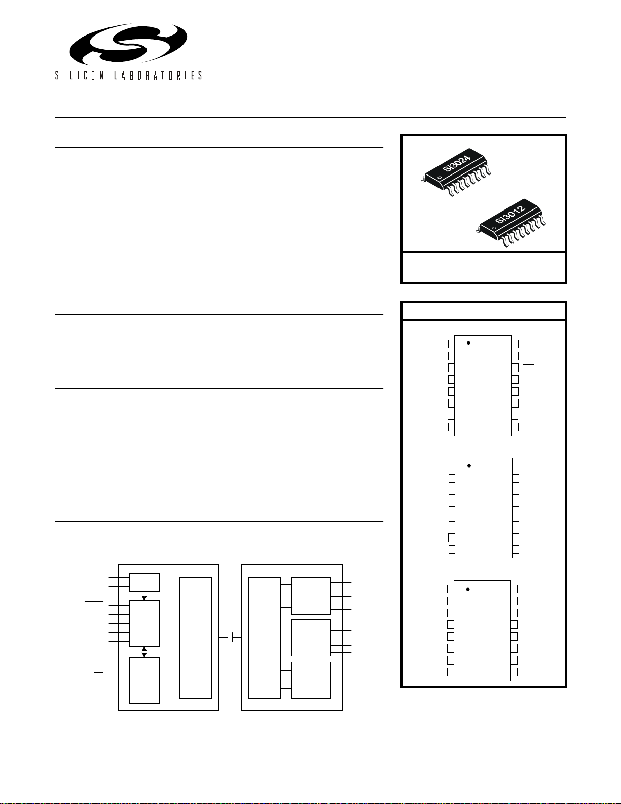
The Si3036 is an integrated direct access arrangement (DAA) chipset that
provides a digital, pr ogrammable interface to a telephone line. Availabl e
in two 16-pin small outline packages (AC’97 interface on Si3024 and
phone-line interface on Si3012), the chipset eliminates the need for an
analog front end (AFE), an isolation transformer, relays, opto-isolators,
and a 2- to 4-wire hybrid. The Si3036 dramatically reduces the number of
discrete components and cost required to achieve compliance with FCC
Part 68 and JATE. The Si3024 complies with the AC’97 2.1 specification.
Functional Block Diagram
Si3024 Si3012
Ordering Information
See page 50.
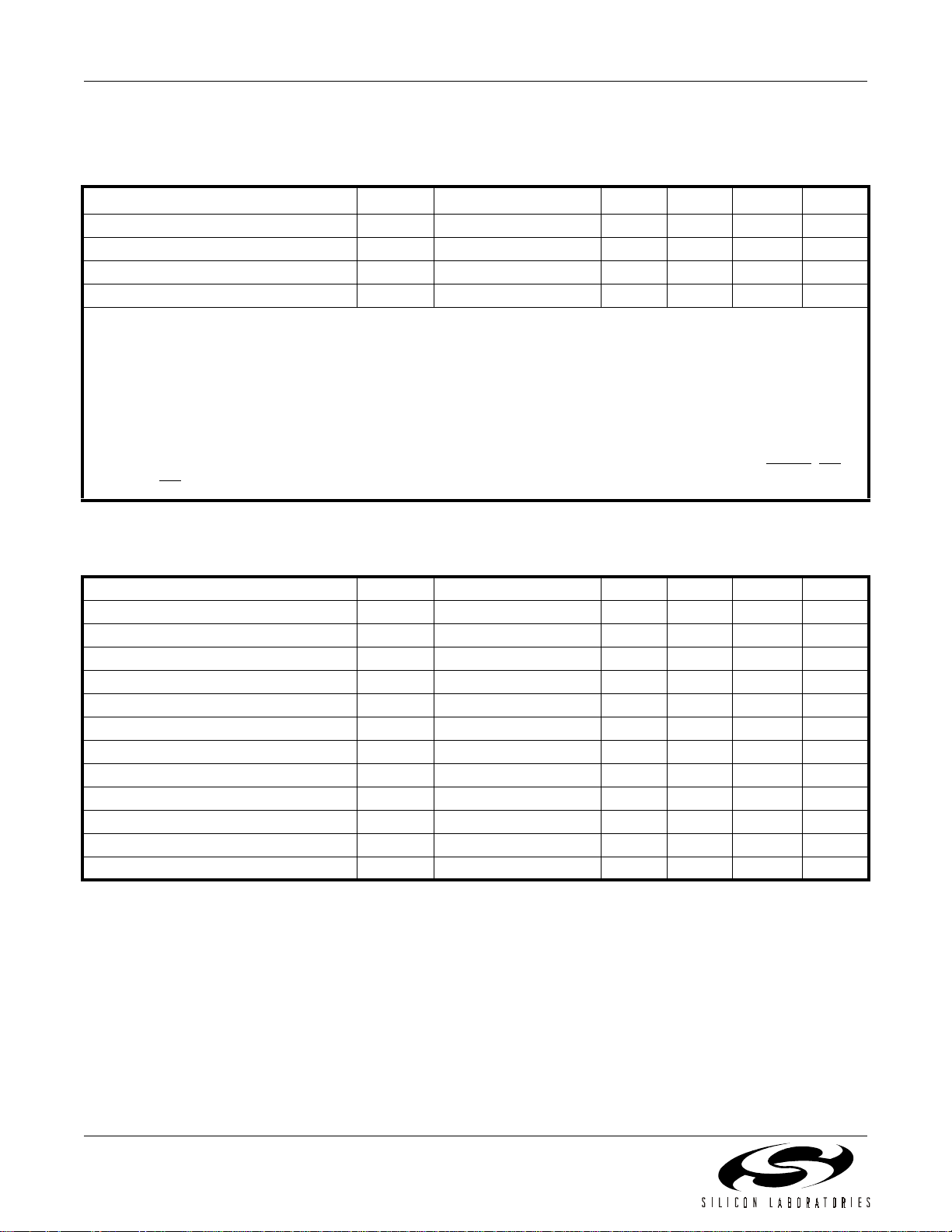
Pin Assignments
Si3024 (SOIC)
MCLK/XIN
XOUT
BIT_CLK
SDATA_IN
SDATA_OUT
SYNC
RESET
SDATA_IN
SDATA_OUT
SYNC
RESET
AOUT
1
2
3
4
V
D
5
6
7
8
Si3024 (TSSOP)
1
2
3
4
5
6
ID0
7
C1A
8
GND
16
15
14
13
12
11
10
16
15
14
13
12
11
10
9
9
GPIO_A
GPIO_B
ID1
V
A
GND
C1A
ID0
AOUT
V
D
BIT_CLK
XOUT
MCLK/XIN
GPIO_A
GPIO_B
ID1
V
A
XOUT
MCL K /X IN
RESET
BIT_CLK
SYNC
SDATA_IN
SDATA_OUT
IDO
ID1
GPIO_A
GPIO_B
Clock
AC'97
Digital
Interfa ce
Control
Interfa ce
Isolation
Interfa ce
Isolation
Interfa ce
Hybrid
DC
Termination
Ring Detect
Off-Hook
Out
TX
In
RX
HYBD
VREG2
VREG
DCT
REXT
IGND
RNG1
RNG2
QB
QE
Si3012 (SOIC or TSSOP)
TSTA
TSTB
IGND
RNG1
RNG2
C1B
QB
QE
1
2
3
4
5
6
7
8
16
15
14
13
12
11
10
9
TX
NC
RX
REXT
DCT
HYBD
VREG2
VREG
US Patent # 5,870,046
US Patent # 6,061,009
Other Patents Pending
Rev. 1.2 12/00 Copyright © 2000 by Silicon Laboratories Si3036-DS12
Page 2

Si3036
2 Rev. 1.2
Page 3

Si3036
T
ABLE OF
C
ONTENTS
Section Page
Electrical Specifications . . . . . . . . . . . . . . . . . . . . . . . . . . . . . . . . . . . . . . . . . . . . . . . . . 4
Typical Application Circuit . . . . . . . . . . . . . . . . . . . . . . . . . . . . . . . . . . . . . . . . . . . . . . . 15
Si3036 Schematic . . . . . . . . . . . . . . . . . . . . . . . . . . . . . . . . . . . . . . . . . . . . . . . . . . . 15
Bill of Materials . . . . . . . . . . . . . . . . . . . . . . . . . . . . . . . . . . . . . . . . . . . . . . . . . . . . . . 16
Analog Output . . . . . . . . . . . . . . . . . . . . . . . . . . . . . . . . . . . . . . . . . . . . . . . . . . . . . . 17
Functional Description . . . . . . . . . . . . . . . . . . . . . . . . . . . . . . . . . . . . . . . . . . . . . . . . . . 18
Initialization . . . . . . . . . . . . . . . . . . . . . . . . . . . . . . . . . . . . . . . . . . . . . . . . . . . . . . . . 18
AC-Link . . . . . . . . . . . . . . . . . . . . . . . . . . . . . . . . . . . . . . . . . . . . . . . . . . . . . . . . . . . 18
JATE Support . . . . . . . . . . . . . . . . . . . . . . . . . . . . . . . . . . . . . . . . . . . . . . . . . . . . . . . 18
Isolation Barrier . . . . . . . . . . . . . . . . . . . . . . . . . . . . . . . . . . . . . . . . . . . . . . . . . . . . . 18
Off-Hook . . . . . . . . . . . . . . . . . . . . . . . . . . . . . . . . . . . . . . . . . . . . . . . . . . . . . . . . . . . 18
Ring Detect . . . . . . . . . . . . . . . . . . . . . . . . . . . . . . . . . . . . . . . . . . . . . . . . . . . . . . . . 19
Wake-Up on Ring . . . . . . . . . . . . . . . . . . . . . . . . . . . . . . . . . . . . . . . . . . . . . . . . . . . . 19
Pulse Dialing . . . . . . . . . . . . . . . . . . . . . . . . . . . . . . . . . . . . . . . . . . . . . . . . . . . . . . . 20
On-Hook Line Monitor . . . . . . . . . . . . . . . . . . . . . . . . . . . . . . . . . . . . . . . . . . . . . . . . 20
Caller ID . . . . . . . . . . . . . . . . . . . . . . . . . . . . . . . . . . . . . . . . . . . . . . . . . . . . . . . . . . . 20
Loop Current Monitor . . . . . . . . . . . . . . . . . . . . . . . . . . . . . . . . . . . . . . . . . . . . . . . . . 20
Analog Output . . . . . . . . . . . . . . . . . . . . . . . . . . . . . . . . . . . . . . . . . . . . . . . . . . . . . . 21
Gain Control . . . . . . . . . . . . . . . . . . . . . . . . . . . . . . . . . . . . . . . . . . . . . . . . . . . . . . . . 21
Filter Selection . . . . . . . . . . . . . . . . . . . . . . . . . . . . . . . . . . . . . . . . . . . . . . . . . . . . . . 21
In-Circuit Testing . . . . . . . . . . . . . . . . . . . . . . . . . . . . . . . . . . . . . . . . . . . . . . . . . . . . 21
Lightning Test . . . . . . . . . . . . . . . . . . . . . . . . . . . . . . . . . . . . . . . . . . . . . . . . . . . . . . . 21
Safety and Isolation . . . . . . . . . . . . . . . . . . . . . . . . . . . . . . . . . . . . . . . . . . . . . . . . . . 21
Digital Interface . . . . . . . . . . . . . . . . . . . . . . . . . . . . . . . . . . . . . . . . . . . . . . . . . . . . . . . . 22
Si3024 as Secondary Device . . . . . . . . . . . . . . . . . . . . . . . . . . . . . . . . . . . . . . . . . . . 22
Si3024 as Primary MC’97 Codec . . . . . . . . . . . . . . . . . . . . . . . . . . . . . . . . . . . . . . . . 22
Si3024 Connection to the Digital AC’97 controller . . . . . . . . . . . . . . . . . . . . . . . . . . . 22
Clocking . . . . . . . . . . . . . . . . . . . . . . . . . . . . . . . . . . . . . . . . . . . . . . . . . . . . . . . . . . . 22
Resetting Si3036 Chipset . . . . . . . . . . . . . . . . . . . . . . . . . . . . . . . . . . . . . . . . . . . . . . 23
AC-Link Digital Serial Interface Protocol . . . . . . . . . . . . . . . . . . . . . . . . . . . . . . . . . . 23
Codec Register Access . . . . . . . . . . . . . . . . . . . . . . . . . . . . . . . . . . . . . . . . . . . . . . . 27
AC-Link Low Power Mode . . . . . . . . . . . . . . . . . . . . . . . . . . . . . . . . . . . . . . . . . . . . . 29
Control Registers . . . . . . . . . . . . . . . . . . . . . . . . . . . . . . . . . . . . . . . . . . . . . . . . . . . . . . . 30
Appendix—UL1950 3rd Edition . . . . . . . . . . . . . . . . . . . . . . . . . . . . . . . . . . . . . . . . . . . . 45
Pin Descriptions: Si3024 . . . . . . . . . . . . . . . . . . . . . . . . . . . . . . . . . . . . . . . . . . . . . . . . . 46
Pin Descriptions: Si3012 . . . . . . . . . . . . . . . . . . . . . . . . . . . . . . . . . . . . . . . . . . . . . . . . . 48
Ordering Guide . . . . . . . . . . . . . . . . . . . . . . . . . . . . . . . . . . . . . . . . . . . . . . . . . . . . . . . . . 50
SOIC Outline . . . . . . . . . . . . . . . . . . . . . . . . . . . . . . . . . . . . . . . . . . . . . . . . . . . . . . . . . . . 51
TSSOP Outline . . . . . . . . . . . . . . . . . . . . . . . . . . . . . . . . . . . . . . . . . . . . . . . . . . . . . . . . . 52
Contact Information . . . . . . . . . . . . . . . . . . . . . . . . . . . . . . . . . . . . . . . . . . . . . . . . . . . . . 54
Rev. 1.2 3
Page 4
Si3036
Electrical Specifications
Table 1: Recommended Operating Conditions
Parameter
Ambient Temperature
1
3
Si3024 Supply Voltage, Analog V
Si3024 Supply Voltage, Digital
Si3024 Supply Voltage, Digital
Notes:
1.
The Si3036 specifications are guaranteed when the typical application circuit (including component tolerances) of
Figure 19 and any Si3024 and Si3012 are used.
2. All minimum and maximum specifications are guaranteed and apply across the recommended operating conditions.
Typical values apply at nominal supply voltages and an operating temperature of 25°C unless otherwise stated.
3.
The temperature specifications are guaranteed when using the typical application circuit on a 4 sq. in. minimum FR4
PCB. For other materials and smaller form factors, heat dissipation factors may apply. Contact Silicon Laboratories for
more details.
4.
The digital supply, V
operating from 3.3 V. 3.3 V operation applies to both the AC’97 Digital Interface and the digital signals RESET
and ID1
.
4
4
can operate from either 3.3 V or 5.0 V. The Si3024 supports interface to 3.3V logic when
D,
Symbol Test Condition
T
A
A
V
D
V
D
K-Grade 0 25 70 °C
VA = 5 V 4.75 5.0 5.25 V
VA = Charge Pump 3.0 3.3 3.6 V
Min
2
Typ
Max
2
Unit
4.75 5.0 5.25 V
, ID0,
Table 2: Loop Characteristics
(VD = 3.0 to 3.6 V, VA = Charge Pump, TA = 0 to 70°C, See Figure 1)
Parameter Symbol Test Condition Min Typ Max Unit
DC Termination Voltage V
DC Termination Voltage V
DC Ring Current I
DC Ring Current I
AC Termination Impedance Z
Operating Loop Current I
TR
TR
RDC
RDC
ACT
LP
Loop Current Sense Bits LCS LCS = Fh 180 155 — mA
Ring Detect Voltage V
Ring Frequency F
On-hook Leakage Current I
RD
R
LK
Ringer Equivalence Number REN w/ Caller ID — 1.0 1.67
Ringer Equivalence Number REN w/o Caller ID — 0.2 —
IL = 20 mA — — 7.7 V
IL = 105 mA 12 — — V
w/ Caller ID — — 1 mA
w/o Caller ID — — 20 µA
—600— Ω
20 — 120 mA
13 18 26 V
RMS
15 — 68 Hz
VTR = –48 V — — 1 µA
4 Rev. 1.2
Page 5
TIP
+
Si3012 V
TR
600
10 µF
Si3036
Ω
I
L
RING
Note: The remainder of the circuit is identical to the one shown in Figure 19 on page 15.
–
Figure 1. Test Circuit for Loop Characteristics
Table 3: DC Characteristics, V
(VA = 4.75 to 5.25 V, VD = 4.75 to 5.25 V, TA = 0°C to 70°C)
Parameter Symbol Test Condition Min Typ Max Unit
High Level Input Voltage V
Low Level Input Voltage V
High Level Output Voltage V
Low Level Output Voltage V
Input Leakage Current I
Power Supply Current, Analog I
Power Supply Current, Digital I
Total Supply Current, Sleep Mode I
= + 5 V
D
A
IH
IL
OH
OL
L
A
D
+ I
3.5 — — V
——0.8V
IO = –2 mA 2.4 — — V
IO = 2 mA — — 0.4 V
–10 — 10 µA
VA pin — 0.1 2 mA
VD pin — 14 17 mA
D
——1.5mA
Table 4: DC Characteristics, VD = + 3.3 V
(VD = 3.0 to 3.6 V, VA = Charge Pump, TA = 0 to 70°C)
Parameter Symbol Test Condition Min Typ Max Unit
High Level Input Voltage V
Low Level Input Voltage V
High Level Output Voltage V
Low Level Output Voltage V
Input Leakage Current I
Power Supply Current, Digital I
Total Supply Current, Sleep Mode I
A
IH
IL
OH
OL
L
D
+ I
IO = –2 mA 2.4 — — V
IO = 2 mA — — 0.35 V
VD pin — 12 14.5 mA
D
Rev. 1.2 5
2.4 — — V
——0.8V
–10 — 10 µA
—1.53.0mA
Page 6
Si3036
Table 5: AC Characteristics
(VD = 3.0 to 5.25 V, VA = Charge Pump, TA = 0 to 70°C)
Parameter Symbol Test Condition Min Typ Max Unit
Freq Response, Transmit
Transmit Full Scale Level
Freq Response, Receive
Receive Full Scale Level
Dynamic Range
Dynamic Range
4
5
Total Harmonic Distortion
1
2
(0 dB gain) V
1
2,3
(0 dB gain) V
6
F
RT
TX
F
RR
RX
Low –3 dB corner — 16 — Hz
—0.98—V
PEAK
Low –3 dB corner — 16 — Hz
—0.98—V
PEAK
DR VIN = 1 kHz, –3 dBFS 80 86 — dB
DR VIN = 1 kHz, –3 dBFS — 84 — dB
THD VIN = 1 kHz, –3 dBFS — –84 — dB
Dynamic Range (call progress AOUT) DR
THD (call progress AOUT) THD
AO
AO
AOUT Full Scale Level — 0.75V
VIN = 1 kHz 60 — — dB
VIN = 1 kHz — 1.0 — %
—V
A
PP
AOUT Output Impedance — 10 — kΩ
Mute Level (call progress AOUT) –90 — — dBFS
Dynamic Range (Caller ID mode) DR
2
Caller ID Full Scale Level (0 dB gain)
Notes:
1. These characteristics are determined by external components. See Figure 19 on page 15.
2. Parameter measured at TIP and RING of Figure 19 on page 15.
3.
Receive Full Scale Level will produce –0.9 dBFS at SDATA_IN.
4. DR = 3 dB + 20log (RMS signal/RMS noise). Applies to both transmit and receive paths. Measurement bandwidth is
300 to 3400 Hz. Sample rate = 9.6 kHz, loop current = 40 mA.
5. DR = 3 dB + 20log (RMS signal/RMS noise). Applies to both tran smit and rece ive path s. Mea surem ent band widt h is 15
to 3400 Hz. Sample rate = 9.6 kHz, loop current = 40mA.
6.
THD = 20log (RMS distortion/RMS signal). This applies to both the transmit and receive paths.
Sample rate = 9.6 kHz, loop current = 40 mA.
V
CID
VIN = 1 kHz, –13 dBFS — 60 — dB
CID
—0.8—V
PEAK
Table 6: Absolute Maximum Ratings
Parameter Symbol Value Unit
DC Supply Voltage V
Input Current, Si3024 Digital Input Pins I
Digital Input Voltage V
Operating Temperature Range T
Storage Temperature Range T
Note: Permanent device damage may occur if the above Absolute Maximum Ratings are exceeded. Functional operation
should be restricted to the conditions as specified in the operational sections of this data sheet. Exposure to absolute
maximum rating conditions for extended periods may affect device reliability.
6 Rev. 1.2
D
IND
STG
, V
IN
A
A
–0.5 to 6.0 V
± 10 mA
–0.3 to (VD + 0.3) V
–40 to 100 °C
–65 to 150 °C
Page 7
Si3036
Table 7: AC Link Timing Characteristics—Cold Reset
(VD = 3.0 to 3.6 V, VA = Charge Pump, TA = 25°C, CL = 50 pF)
Parameter Symbol Min Typ Max Unit
RESET
RESET
Active Low Pulse Width T
Inactive to BIT_CLK Startup
rst_low
T
rst2clk
1.0 — — µs
162.8 — — ns
Delay
T
rst2clk
T
rst_low
RESET
BIT_CLK
Figure 2. Cold Reset Timing Diagram
Table 8. AC Link Timing Characteristics—Warm Reset
(VD = 3.0 to 3.6 V, VA = Charge Pump, TA = 25°C, CL = 50 pF)
Parameter Symbol Min Typ Max Unit
SYNC Active High Pulse Width T
SYNC Inactive to BIT_CLK Startup Delay T
sync_high
sync2clk
1.0 — — µs
162.8 — — ns
SYNC
BIT_CLK
T
sync_high
T
sync2clk
Figure 3. Warm Reset Timing Diagram
Rev. 1.2 7
Page 8
Si3036
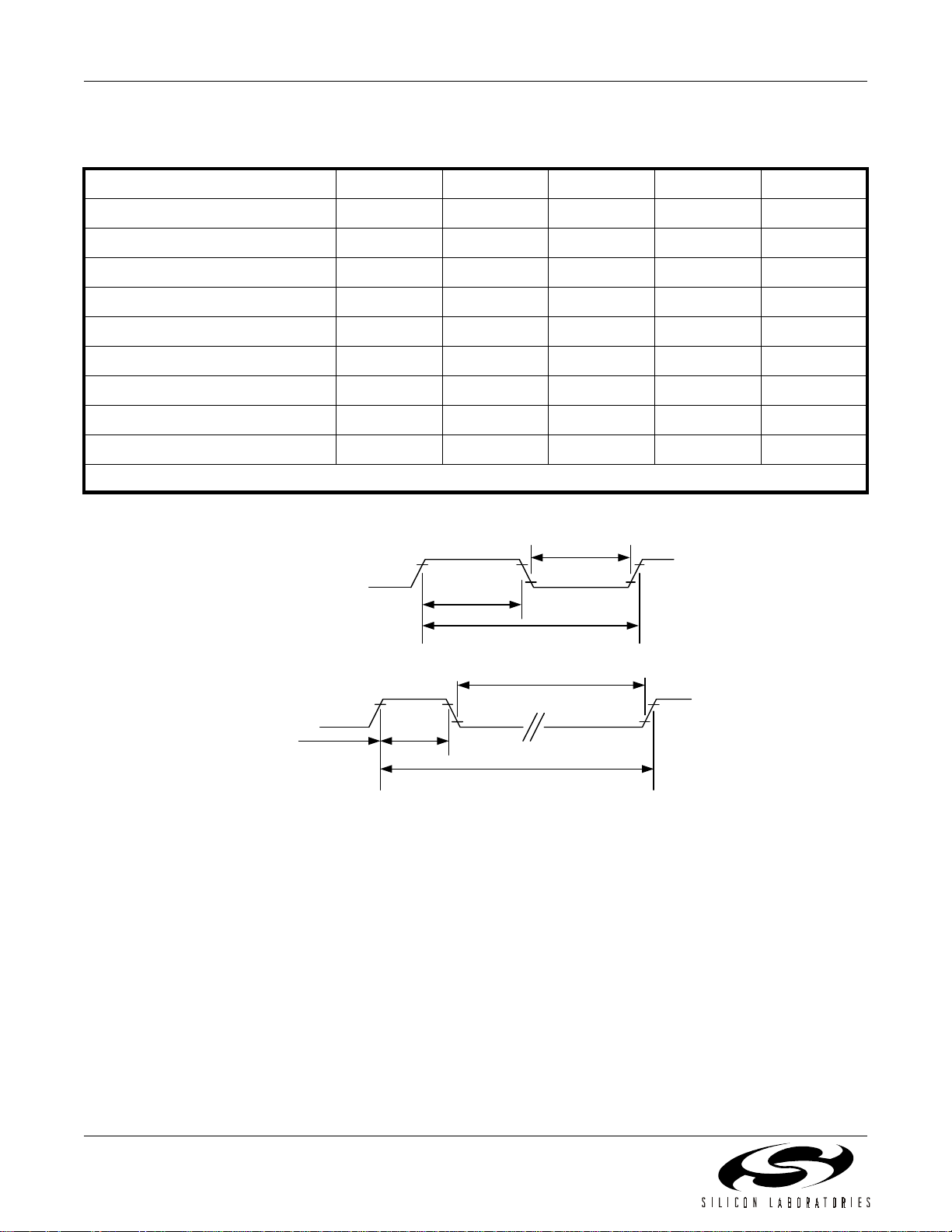
Table 9. AC Link Timing Characteristics—Clocks
(VD = 3.0 to 3.6 V, VA = Charge Pump, TA = 25°C, CL = 50 pF)
Parameter Symbol Min Typ Max Unit
BIT_CLK Frequency — 12.288 — MHz
BIT_CLK Period T
clk_period
— 81.4 — ns
BIT_CLK Output Jitter — — 750 ps
BIT_CLK High Pulse Width* T
BIT_CLK low Pulse Width* T
clk_high
clk_low
36 40.7 45 ns
36 40.7 45 ns
SYNC Frequency — 48.0 — kHz
SYNC Period T
SYNC High Pulse Width T
SYNC Low Pulse Width T
*Note: Worst case duty cycle rest ricted to 45/55.
BIT_CLK
sync_period
sync_high
sync_low
— 20.8 — µs
—1.3—µs
— 19.5 — µs
T
clk_low
T
clk_high
T
clk_period
T
sync_low
SYNC
T
sync_high
T
Figure 4. Clocks Timing Diagram
8 Rev. 1.2
sync_period
Page 9
Si3036
Table 10. AC Link Timing Characteristics—Data Se tup and Hold
(VD = 3.0 to 3.6 V, VA = Charge Pump, TA = 25°C, CL = 50 pF)
Parameter Symbol Min Typ Max Unit
Setup to Falling Edge of BIT_CLK T
Hold from Falling Edge of BIT_CLK T
T
setup
BIT_CLK
SYNC
SDATA_OUT
SDATA_IN
T
hold
setup
hold
15.0 — — ns
5.0 — — ns
Figure 5. Data Setup and Hold Timing Diagram
Table 11. AC Link Rise and Fall Times
(VD = 3.0 to 3.6 V, VA = Charge Pump, TA = 25°C, CL = 50 pF)
Parameter Symbol Min Typ Max Unit
BIT_CLK Rise Time Trise
BIT_CLK Fall Time Tfall
SYNC Rise Time Trise
SYNC Fall Time Tfall
SDATA_IN Rise Time Trise
SDATA_IN Fall Time Tfall
SDATA_OUT Rise Time Trise
SDATA_OUT Fall Time Tfall
clk
clk
sync
sync
din
din
dout
dout
2—6ns
2—6ns
2—6ns
2—6ns
2—6ns
2—6ns
2—6ns
2—6ns
BIT_CLK
SYNC
Trise
Trise
clk
sync
SDATA_IN
Tfall
Tfall
clk
SDATA_OUT
sync
Trise
Trise
din
dout
Figure 6. Signal Rise and Fall Timing Diagram
Rev. 1.2 9
Tfall
Tfall
din
dout
Page 10
Si3036
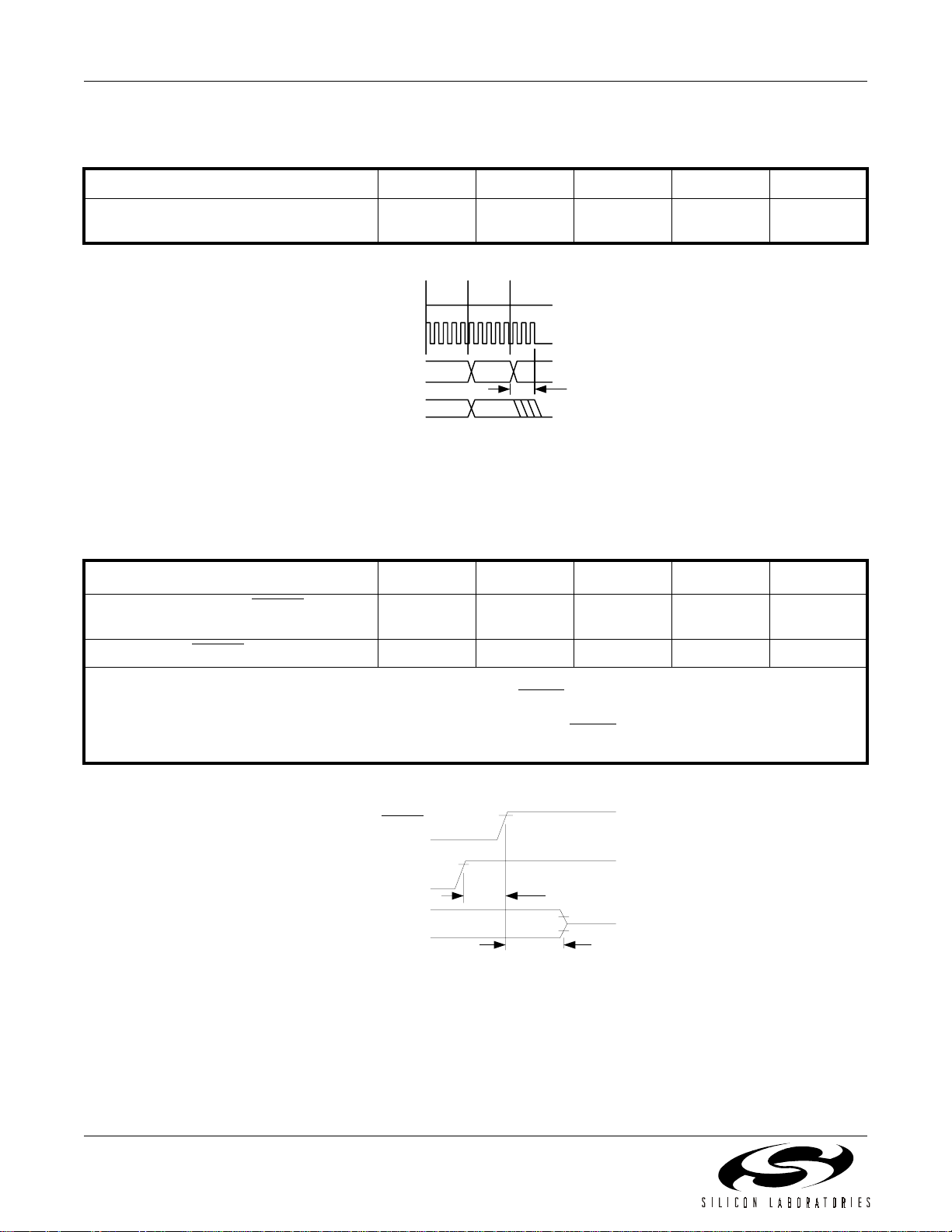
Table 12. AC Link Timing Characteristics— Low Power Mode Timing
(VD = 3.0 to 3.6 V, VA = Charge Pump, TA = 25°C, CL = 50 pF)
Parameter Symbol Min Typ Max Unit
End of Slot 2 to BIT_CLK, SDATA_IN
T
s2_pdown
——1.0µs
Low
SYNC
BIT_CLK
DATA_OUT
SDATA_IN
Slot 1 Slot 2
Write to
Note: B IT_C LK n o t to s c a le
0x56
Data
MLNK
Don't care
Figure 7. AC-Link Low Power Mode Timing Diagram
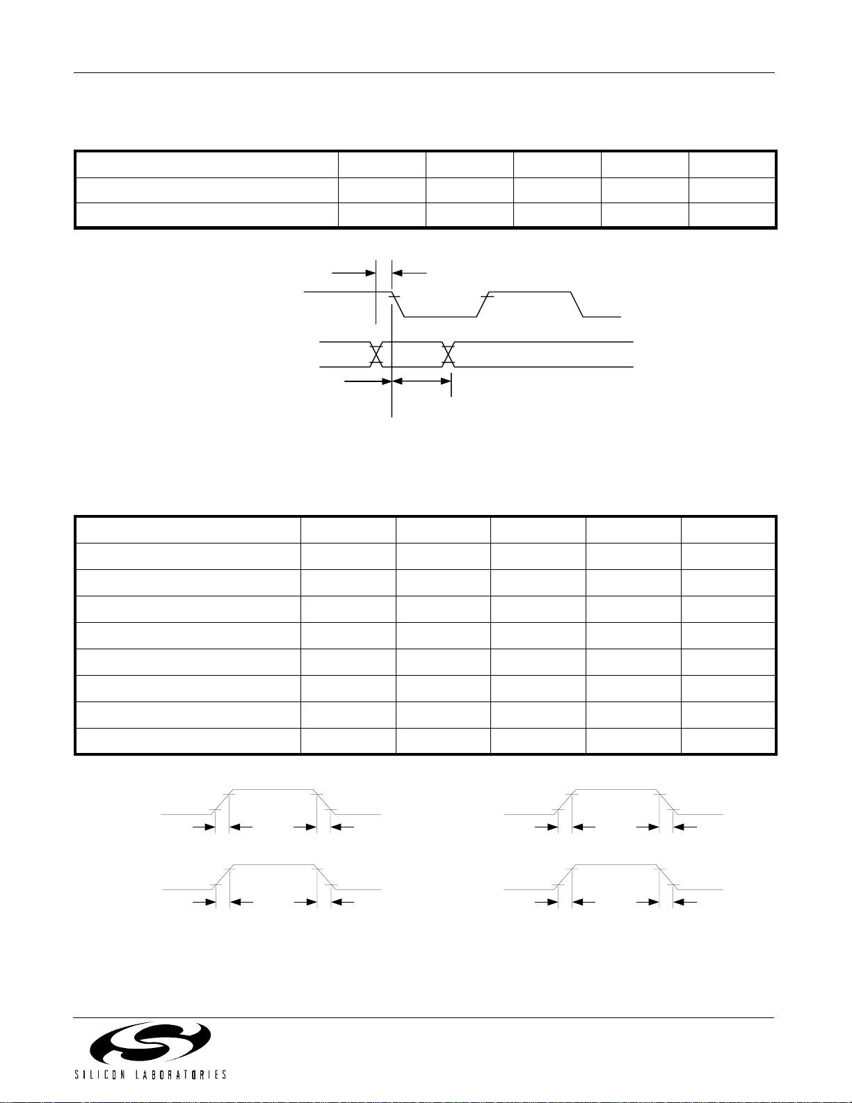
Table 13. ATE Test Mode
(VD = 3.0 to 3.6 V, VA = Charge Pump, TA = 25°C, CL = 50 pF)
Parameter
Setup to falling edge of RESET
1,2
(also
applies to SYNC)
Rising edge of RESET
Notes:
1. All AC link signals are normal ly low th rough the tra iling edge of RESET
of RESET causes AC’97 AC-link outputs to go high impedance, which is suitable for ATE in circuit testing.
2. When the test mode has been entered, AC’97 must be issued another RESET
the normal operating mode.
to Hi-Z delay T
Symbol Min Typ Max Unit
T
setup2rst
off
15.0 — — ns
— — 25.0 ns
T
s2_pdown
. Bringing SDA TA_OUT high for the trailing edge
with all AC-link signals low to return to
RESET
SDATA_OUT
SDATA_IN, BIT_CLK
T
off
Figure 8. ATE Test Mode Timing Diagram
10 Rev. 1.2
T
setup2rst
Hi-Z
Page 11
Table 14: Digital FIR Filter Characteristics—Transmit and Receive
(VD = 3.0 to 3.6 V, VA = Charge Pump, Sample Rate = 8 kHz, TA = 70°C)
Parameter Symbol Min Typ Max Unit
Si3036
Passband (0.1 dB) F
Passband (3 dB) F
(0.1 dB)
(3 dB)
0—3.3kHz
0—3.6kHz
Passband Ripple Peak-to-Peak –0.1 — 0.1 dB
Stopband — 4.4 — kHz
Stopband Attenuation –74 — — dB
Group Delay t
Note: Typical FIR filter characteristics for Fs = 8000Hz are shown in Figures 9, 10, 11, and 12.
gd
— 12/Fs — sec
Table 15: Digital IIR Filter Characteri stics—Transmit and Receive
(VD = 3.0 to 3.6 V, VA = Charge Pump, Sample Rate = 8 kHz, TA = 70°C)
Parameter Symbol Min Typ Max Unit
Passband (3 dB) F
(3 dB)
Passband Ripple Peak-to-Peak –0.2 — 0.2 dB
Stopband — 4.4 — kHz
Stopband Attenuation –40 — — dB
Group Delay t
Note:
Typical IIR filter characteristics for Fs = 8000 Hz are shown in Figures 13, 14, 15, and 16. Figures 17 and 18 show
group delay versus input frequency.
gd
0—3.6kHz
— 1.6/Fs — sec
Rev. 1.2 11
Page 12
Si3036
Attenuation—dB
Input Frequency—Hz
Figure 9. FIR Receive Filter Response
Attenuation—dB
Input Frequency—Hz
Figure 10. FIR Receive Filter Passband Ripple
Attenuation—dB
Input Frequency—Hz
Figure 11. FIR Transmit Filter Response
Attenuation—dB
Input Frequency—Hz
Figure 12. FIR Transmit Filter Passband Ripple
For Figures 9–12, all filter plots apply to a sample rate of
Fs = 8 kHz. The filters scale with the sample rate as follows:
F
where Fs is the sample frequency.
12 Rev. 1.2
(0.1 dB)
F
(–3 dB)
= 0.4125 Fs
= 0.45 Fs
Page 13
Si3036
Attenuation—dB
Input Frequency—Hz
Figure 13. IIR Receive Filter Response
Attenuation—dB
Input Frequency—Hz
Figure 14. IIR Receive Filter Passband Ripple
Attenuation—dB
Input Frequency—Hz
Figure 15. IIR T ransmit Filter Response
Attenuation—dB
Input Frequency—Hz
Figure 16. IIR Transmit Filter Passband Ripple
For Figures 13–16, all filter plots apply to a sample rate of
Fs = 8 kHz. The filters scale with the sample rate as follows:
F
where Fs is the sample frequency.
= 0.45 Fs
(–3 dB)
Rev. 1.2 13
Page 14
Si3036
Delay—µs
Input Frequency—Hz
Figure 17. IIR Receive Group Delay
Delay—µs
Input Frequency—Hz
Figure 18. IIR Transmit Group Delay
14 Rev. 1.2
Page 15
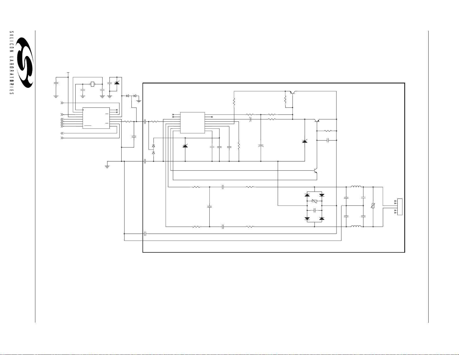
Typical Application Circuit
+3.3VD
C10
ID1#
BITCLK
SDATA_IN
SDATA_OUT
SYNC
RESET#
AOUT
ID0#
Rev. 1.2 15
24.576 MHz
Y1
1
MCLK/XIN
2
XOUT
3
BIT_CLK
4
VD
5
SDATA_IN
6
SDATA_OUT
7
SYNC
89
RESET AOUT
Si3024
C3
GND
Z4
D3
BAV99
16
15
14
ID1
13
VA
12
11
C1A
10
ID0
R27
C30
C35C34
U1
GPIO_A
GPIO_B
No Ground Plane In DAA Section
1
TSTA
2
TSTB
C1
R28
BAV99
C2
3
IGND
4
C1B
5
RNG1
6
RNG2
7
QB
89
QE VREG
Z5D4
Si3012
Q1
R1
U2
16
TX
15
NC
14
RX
13
REXT
12
DCT
11
HYBD
10
VREG2
C6
C12
C16
R4
+
C5
R2
+
R5
R21
R18
C23
Q2
R6
C20
Z1
Q3
Note1: If JATE support is not required, R21,
C12 and C23 may be removed and the
following modifications implemented: R21
should be replaced with a 0 ohm resistor or
shorted, and R4 should be changed to a 604
ohm, 1/ 4 W, +- 1%.
Note 2: See Appendix for applications
requiring UL 1950 3rd Edition compliance.
R23
R22
C4
C8
C11
C7
R10
R9
Figure 19. Typical Application Circuit for the Si3036
FB2
D1
RV2
C9
D2
C32
C25
RV1
C24
C31
FB1
J1
1
2
3
4
5
6
RJ-11
Si3036
Page 16

Si3036
Bill of Materials
Table 16. FCC Component Values—Si3036 Chipset
Component
C1,C4 150 pF, 3 kV, X7R, ±20% Novacap, Venkel, Johanson, Murata, Panasonic
C2 Not Installed
C3 0.22 µF, 16 V, X7R, ±20%
C5 1 µF, 16 V, Tant/Elec, ±20%
C6,C10,C16 0.1 µF, 16 V, X7R, ±20%
C7,C8,C9 15 nF, 250 V, X7R, ±20% Novacap, Johanson, Murata, Panasonic
C11 39 nF, 16 V, X7R, ±20%
C12
C23
C24,C25,C31,C32
C30
C34,C35
D1,D2
D3,D4
FB1,FB2 Ferrite Bead Murata
Q1,Q3 A42, NPN, 300 V OnSemiconductor, Fairchild
Q2 A92, PNP, 300 V OnSemiconductor, Fairchild
RV1 Sidactor, 275 V, 100 A Teccor, ST Microelectronics, Microsemi, TI
RV2 MOV, 240 V Panasonic
R1 51 Ω, 1/2 W ±5%
R2 15 Ω, 1/4 W ±5%
R42,R18,R21
R5,R6 36 kΩ, 1/10 W ±5%
R9,R10 2 kΩ, 1/10 W ±5%
R22,R23 20 kΩ, 1/10 W ±5%
R27,R28 10 Ω, 1/10 W ±5%
U1 Si3024 Silicon Labs
U2 Si3012 Silicon Labs
Y1
Z1 Zener diode, 18 V Vishay, Rohm, OnSemi
Z4,Z5 Zener diode, 5.6 V, 1/2 W Diodes Inc., OnSemiconductor, Fairchild
Notes:
1. The following referenc e des ignato rs were i ntentio nally omitt ed: C 13–C15, C17– C22, C2 6–C29, C 31–C3 3, R3 , R7,
R8, R11–R17, R19, and R20.
2. If JA TE suppo rt is not requi red, R21 , C12, and C2 3 may be remov ed and the fol lowing modific ations imple mented:
R21 should be replaced with a 0 Ω resistor or shorted, and R4 should be changed to a 604 Ω, 1/4 W, ±1%.
3. Alternate population option is C24, C25 (2200 pF, 3 kV, X7R, ±10% and C31, C32 not installed).
4. Install only if needed for improved radiated emissions performance (10 pF, 16 V, NPO, ±10%).
5. Y1, C34, and C35 should be installed if the Si3024 is configured as a primary device.
6. Several diode bridge configurations are acceptable (suppliers include General Semi, Diodes Inc.)
1
2
2
3
4
5
6
2
4
2.7 nF, 16 V, X7R, ±20%
0.1 µF, 16 V, Tant/Elec/X7R, ±20%
1000 pF, 3 kV, X7R, ±10% Novacap, Venkel, Johanson, Murata, Panasonic
33 pF,16 V, NPO, ±5% Novacap, Venkel, Johanson, Murata, Panasonic
Dual Diode, 300 V, 225 mA Central Semiconductor
BAV99 Dual Diode, 70 V, 350 mW Diodes Inc., OnSemiconductor, Fairchild
24.576 MHz, 18 pF, 50 ppm
Value Supplier(s)
Not Installed
301 Ω, 1/10 W, ±1%
16 Rev. 1.2
Page 17

Si3036
Analog Output
Figure 20 illustrates an option al application circuit to support the analog outp ut capability of the Si3036 for call
progress monitoring purp os es. Th e AO UT le ve l ca n be s et to 0 dB , –6 dB, –12 dB, and mute for both tran sm it and
receive paths through the ATM/ARM bits in Register 5Ch. U1 provides a gain of 26 dB. Additional gain adjustments
may be made by varying the voltage divider created by R1 and R3.
+5 V
AOUT
C2 R3
C6C1
R1
326
+
–
C4
5
U1
4
C3
+
C5
Speaker
R2
Figure 20. Optional Connection to AOUT for a Call Progress Speaker
‘
Table 17. Component Values—Optional Connection to AOUT
Symbol Value
C1 2200 pF, 16 V, ±20%
C2, C3, C5 0.1 µF, 16 V, ±20%
C4 100 µF, 16 V, Elec. ±20%
C6 820 pF, 16 V, ±20%
R1 10 kΩ, 1/10 W, ±5%
R2 10 Ω, 1/10 W, ±5%
R3 47 kΩ, 1/10 W, ±5%
U1 LM386
Rev. 1.2 17
Page 18

Si3036
Functional Description
The Si3036 is an integrat ed ch ip se t that pr ov id es a lowcost, isolated, silicon-based MC97-compliant interface
to the telephone line. The chipset reduces cost and
board area by eliminating the need for a modem AFE or
serial codec. It also elim inates the need fo r an isolatio n
transformer, relays, opto-isolators, and a 2- to 4-wire
hybrid. The Si3036 complies with the AC’97 2.1
specification an d requires only a few low-cost discret e
components to achieve full compliance with FCC Part
68 and JATE out-of-band noise requirements. See
Figure 19 on page 15 for a typical application circuit.
See the pin-compatibl e Si3038 data sheet for designs
requiring global compliance.
Initialization
When the Si3036 is initially powe re d up, the R ES ET pin
should be asserted. When the RESET
deasserted, the regi sters will have default values. This
reset condition gua ra nte es th e li ne- s id e ch ip ( Si3012) is
powered down with no possibility of loading the line (i.e.,
off-hook). An example initialization procedure is outlined
below:
1. Execute a register reset by writing (any value) to
Register 3Ch.
2. Program the desired sample rate with Register 40h (42h).
See Register 40h (42h) description on page 33 for
allowable sample rates.
3. Write 0x0000 to Register 3Ch to power up the Si3036.
4. Wait for the Si3036 to complete power up. The lower 8 bits
indicate that the Si3036 is ready. If the Si3036 is
configured as line #1 codec, 3Eh[7:0] = 0x0F indicates
readiness. If the codec is configured as line #2,
3Eh[7:0] = 0x33 indicates readiness.
5. Program GPIO registers to desired modes (registers 4Ch–
54h).
6. Program DAC/ADC levels with Register 46h (48h).
After this procedure is comp lete, the Si3036 is ready for
ring detection and off-hook operation.
AC-Link
AC-link is a b idirectional, fixed rate, seria l PCM digital
stream. It handles multiple input and output audio
streams and control register accesses employing a time
division multiplexed (TDM) scheme. The AC-link
architecture divi des each audio frame into 12 outgoing
and 12 incoming dat a strea ms, ea ch wi th 20- bit sam ple
resolution.
The AC-link serial interconnect defines a digital data
and control pipe between the control ler and the codec.
The AC-link supports 12 20-bit slots at 48 kHz on
SDATA_IN and SDATA_OUT. The TDM “slot-based”
pin is
architecture suppo rts a per-slot valid tag infrastructure
that is the source of each slot’s data sets or clears to
indicate the validity of the slot data within the current
frame. For modem AFE, data streams at a variety of
required sample rates can be supported.
JATE Support
Capacitor C23 adds the nece ssary transmit ou t-of- band
filtering required to meet JATE out-of-band noise
specifications. The addition of C23 alters the transmit
path frequency res ponse which must be b alanced with
capacitor C12 to obtain maximum hybrid cancellation.
Products using th e Si3036 which have b een submitted
for JATE approval should document a waiver for the
JATE DC Terminatio n spec ificati on. Thi s sp ecifica tio n is
met in the Si3038 global DAA device.
Isolation Barrier
The Si3036 achieves an isolation barrier through lowcost, high-volta ge capacitors in co njunction with Si licon
Laboratories’ patented ISOcap signal processing
techniques. These techniques eliminate any signal
degradation due to capacitor mismatches, common
mode interference, or noise coupling. As shown in
Figure 19 on page 15, the C1, C2, C4, C24, and C25
capacitors isolate the Si3024 (system-side) from the
Si3012 (line-side). All transmit, receive, control, ring
detect, and caller ID data are communicated through
this barrier.
The ISOcap communic ations l ink is d isabled by def ault.
The PR bits in Register 3Eh mus t be cleared, and the
sample rate must be set in Register 40h/42h. No
communication between the Si3024 and Si3012 can
occur until these conditions are set.
Off-Hook
The communication system generates an off-hook
command by writing a logic 1 to GPIO0 (line 1) or
GPIO10 (line 2) of slot 12. T he off-hook s tate is used to
seize the line for an incoming/outgoing call and can also
be used for pulse dialing. When in the on-hook state,
negligible DC current fl ows through the hookswitch. In
the off-hook state, the h ookswitch transistor p air, Q1 &
Q2, turn on.
The net effect of the off-hook signal i s the applic ation of
a termination impe dance a cross TIP and RING and th e
flow of DC loop current. The termination impedance has
both an AC and DC component.
The AC termination impedance is a 604-Ω resistor,
which is connected to the TX pin. The DC termination is
a 51-Ω resistor, which is connected to the DCT pin.
When executing an off-hook sequence, the Si3036
18 Rev. 1.2
Page 19

Si3036
requires 1548/Fs secon ds to comp lete the off-hook an d
provide phone line data on the AC link. This includes
the 12/Fs filter group delay. If necessary , for the shortest
delay, a higher Fs may be established prior to executing
the off-hook. The delay allows line transients to settle
prior to normal use.
Ring Detect
The ring signal enters the Si3036 through low-value
capacitors (C7 and C8) connected to TIP and RING.
The integrated ring detect of the Si3036 chipset allows it
to present the ring signal to the AC’97 controller through
the AC-link with no additional signaling required. The
signal sent to the AC’97 controller is a clipped version of
the original ring signal. In additi on, the Si3036 passes
through the caller ID data unaltered.
The system can detect a ring occur ring by the status of
the GPIO1 (GPIO11) bit of slot 12. This bit is set when
the line-side device detec ts a ring signal at RNG1 and
RNG2. When this state occurs, the line-side chi p draws
a small amount of DC current from the line to provide
the digitized line data to the AC’97 controller. The
GPIO1 (GPIO11) bit clears when the system either goes
off-hook or 4.5 to 9 seconds after the last ring is
detected.
The ring information is passed to the AC’97 controller
via the SDATA_IN pin. SDATA_IN will be –32768
(8000h) while the R NG1-RNG2 voltage is between the
ring thresholds. When a r ing i s d ete cte d, S DATA_IN will
transition rather quickly to +32767 w hile the ring signal
is positive, then go back to –32768 while the ring is near
zero and negative. Thus a near square wave is
presented on SDATA_IN that swings from –32768 to
+32767 in cadence with the ring signal.
Wake-Up on Ring
Ring is an example of an event that might need to wakeup a PC that has suspended into a low-power state.
Power management (or wake) event support for a
modem is a key feature of the current PC industry
standards.
The Si3036 provides wake-up on ring through the AClink as defined by the AC’ 97 ver 2.1 specifi cation. In an
implementation designed for wake-on ring where the
Si3036 and AC-link are both completely powered by
Vaux, a ring detec ted at the RNG1 and RNG2 pins o f
the Si3036 causes the assertion of the power
management signal to the system. The power
management signal i s the risin g edge of the SDATA_IN
signal when the Si3036 is in low-power mode. The
power management eve nt signal assertion causes the
system to resume so that the modem event (ring) can
be serviced. The first thi ng that the device driver must
do to reestablish communicati ons with the Si3036 is to
command the AC’97 Digital Controller to execute a
warm reset to the AC-link. Figure 21 illustrates the
entire sequence.
The rising edge of SDATA _IN causes the AC’97 Digital
Controller to assert its pow er mana gement signal to th e
system’s ACPI controller. The Si3036 will keep
SDATA_ IN high unti l it has sam pled SY NC havin g gone
high, and then low (warm reset). The power
management event is cleared out in the AC’97 Digital
Controller by system so ftware, asynchr onous to AC-link
activity. The AC’97 Digital Controller should always
monitor the Si3036’s ready bi t before sen ding da ta to it.
The modem driver should read the GPIO Pin Status
register to determine i f the wake event was due to the
ring signal before executing a register reset.
Before entering the low-power mode, the Si 3036 must
be enabled to cause the wa ke signal when receivin g a
ring. This is done by programmi ng the GPIO Pin Sticky
(50h) and GPIO Wake Up Mask (52h) registers and
clearing previous sticky GPIO events. Before setting the
MLNK bit the driver should do the following:
1. Set the GS1 bit in Register 50h (GS11 if using line #2).
2. Set the GW1 bit in Register 52h (GW11 for line #2).
3. Clear a possible old sticky event by writing a 0 to the GI1
(GI11 for line #2) bit in the read-only register—GPIO Pin
Status register (54h).
SYNC
BIT_CLK
SDATA_OUT
SDATA_IN
slot 12
prev. frame
slot 12
prev. frame
Power Down Frame Sleep State
Write to
TAG
TAG
Data
56th
MLNK
Wake Event
Figure 21. AC-Link Power-Down/Up Sequence
Rev. 1.2 19
New Audio Frame
TAG Slot 1 Slot 2
TAG Slot 1 Slot 2
Page 20

Si3036
If the AC’97 Digital Controll er allows the RESET sig nal
to go low during the low-p ower mode of the Si 3036, th e
wake event will be a cold reset (rising edg e of RESET
and the modem driver sh ould reprogram the GPIO P in
Sticky register to set the GS1 (or GS11) bit. This will
allow the modem driv er to read the sticky value of the
GPIO Pin Status register.
The Si3036 can also be programmed to wake up on
events due to GPIO_A and GPIO_B.
Pulse Dialing
Pulse dialing is acc omplished by going off and on hook
to generate make and break pulses. The nominal rate is
10 pulses per second.
The Si3036 DC holding circ uit has active control of th e
on-hook and off-hook transients to maintain pulse
dialing fidelity.
On-Hook Line Monitor
The Si3036 allows the user to receive line activity when
in an on-hook state. T he LINE1_CID/LINE2_CID bit in
slot 12 enables a low-power ADC which digitizes the
signal passed across the RNG1/2 pins. This signal is
passed across the AC-link to the AC’97 controller. A
current of approx imately 450 µA is drawn fr om the line
when this bit is activated. This mode is typically used to
detect caller ID data (see the “Caller ID” section).
The on-hook line monitor can also be used to detect
whether a phone line is physically connected to the
Si3012 and associ ated circuitry. If a line is present and
the LINE1_CID/LINE2_CID bit is set, SDATA_IN will
have a near zero value and th e LCS[3:0] bits will read
1111b. Due to the nature of the low-power ADC, the
data presented on SDATA_IN could have up to a 10 %
DC Offset.
If no line is connected, the output of SDATA_IN will
move towards a negative ful l scale v alue (–32 768). Th e
value is guaranteed to be at least 89% of negative f ull
scale. In addition, the LCS[3:0] bits will be zero.
Caller ID
Using the on-hook line monitor feature, the Si3036
provides the designer with the ability to pass caller ID
data from the p ho ne line to th e AC- li nk in t erf ac e.
In countries where the caller ID data is passed on the
phone line between the first and second rings, the
following metho d should be utilized to capture the caller
ID data. The LINE1_CID/LINE2_CID bit (GPIO2/12 in
slot 12) should be set upon completion of the first ring
signal. This b it en ab le s a low-power ADC (a pp rox i ma tel y
450 µA is drawn from the line) whi ch digitizes the sign al
passed across the RNG1/2 pins. This signal is passed
across the ISOcap to the AC-link interface. The
LINE1_CID/LINE2_CID bit should be cleared after the
caller ID data is received and prior to the second ring.
),
Due to the nature of the low-power ADC, the data
presented on SDA TA_IN will have up to a 10% DC Offset.
The caller ID decoder must use either a high pass or band
pass filter to accurately retrieve the caller ID data.
Loop Current Monitor
It may be desirabl e to have a meas urement of t he loop
current being drawn from the li ne. This measurements
can be used to tell whether a telephone line is
connected, whether a pa rallel hands et has been picked
up, or if excessive loop current is present.
When the system is in an off-hook sta te, the LCS bits of
Register 5Eh indicate the approximate amount of DC
loop current. The LCS is a 4-bit va lue ran gi ng from z er o
to fifteen. Each unit represents approximately 6 mA of
loop current from LCS codes 1–14. The typical LCS
transfer function is shown in Figure 22:
15
10
LCS
BIT
5
0
0 6 12 18 24 30 36 42 48 54 60 66
Figure 22. Typical LCS Transfer Function
An LCS value of zero means the loop current is less
than required for normal operation and the system
should be on-hook. Typically, an LCS value of 15 means
the loop current is greater than 155 mA.
The LCS detector has a built-in hysteresis of 2 mA. This
allows for a stab le LCS value wh en the loop current is
near a transition level. The LCS value is a rough
approximation of the l oop current, and the designer is
advised to use this value in a relative means rather than
an absolute value.
This feature enables the modem to determine if an
additional line has “picked up” while the modem is
transferring informat ion. In the case of a second phon e
going off-hook, the loop current falls approximately 50%
and is reflected in the value of the LCS bits.
72
78 84 90 96
Loop Current (mA)
155
20 Rev. 1.2
Page 21

Si3036
Analog Output
The Si3036 supports an analog output (AOUT) for
driving the call progress speaker. AOUT is an analog
signal comprise d of a mix of the transmit and receive
signals.
The AOUT level can be adj usted v ia the ATM and ARM
bits in control Register 5Ch. The transmit portion of
AOUT can be set to –2 0 dB , –26 dB, –32 dB, or mute.
The receive portion of AOUT ca n be set to 0 dB, –6 dB,
–12 dB, or mute. Figure 20 on page 17 illustrates a
recommended application circuit. Note that in the
configuration shown, the LM386 provides a gain of
26 dB. Additional gain adjustments may be made by
varying the voltage divider created by R1 and R3.
Gain Control
The Si3036 supports multiple gain and attenuation
settings in Register 46h/48h for the receive and transmit
paths, respectively. The receive path can suppor t gains
of 0, 3, 6, 9, and 12 dB, as selected by A DC[3:1] bits.
The receive path can also be muted by setting bit 7. The
transmit path can su ppo rt attenuations of 0, 3, 6, 9, an d
12 dB, as selected by DAC[3:1] bits. The tran smit path
can also be muted by setting bit 15.
Filter Selection
The Si3036 supports addit ional filter selections for the
receive and transmit signals. The IIRE bit of
Register 5Ch, when set, enables the IIR filters. This
filter provides a much lower, however non-linear, group
delay than the default FIR filters.
In-Circuit Testing
T
he Si3036’s advanced design provides the modem
manufacturer with increased ability to determine system
functionality during production line tests, as well as user
diagnostics. Several loopback modes exist allowing
increased coverage of system components.
The loopback mode allows the data pum p to provide a
digital input test pattern on SDATA_IN and receive a
corresponding di git al tes t p atte rn ba ck o n S DATA_OUT.
To enable this mode, set L1B[2:0] (L2B[2:0])=101 in
Register 56h. In this mode, the isolation barrier is
actually being tested. The digital stream is delivered
across the isolation capa citors, C1 and C2 of Figu re 19
on page 15, to the line-side dev ice and retur ned acro ss
the same barrier.
The digital DAC loopback mode al lows data to be sent
on the digital path from SDATA_IN to the digital section
of DAC to ADC to SDATA_OUT. This loopback mode is
used when the line-side chip is in power-down mode. To
enable this mode, set L1B[2:0] (L2B[2:0])=011 in
Register 56h.
The remote analog loopback mode allows an external
device to drive the recei v e pins of th e l ine -si de chi p an d
receive the signal from the transmit pins. This mode
allows testing of external components connecting the
RJ-11 jack (TIP and RING) to the line side of the
Si3012. To enable this mode, set L1B[2: 0] (L2B[2:0]) =
100 in Register 56h.
The ADC loopback mode allows an external device to
drive the receive pins of th e Si3012. The signal is then
digitized on the Si3012 and sent to the Si3024, which
sends the data back to the S i3012. The signal is then
converted back to analog. The external dev ice receives
the signal on the transmit pins. This mode allows testing
of the Si3036s converters and external devices between
the Si3012 and RJ-11 jack. To enable this mode, set the
L1B[2:0] (L2B[2:0]) = 001.
The final two testi ng modes, lo cal analog loopback an d
external analog loopb ack, allow the system to test the
basic operation of the converters on the line side and
the functionality of the external components. In local
analog loopback mod e, the AC’97 controlle r provides a
digital test waveform on SDATA_OUT. This data is
passed across the isolation barrier, converted to analog,
internally looped to the receive path, converted to
digital, passed back across the isolation barrier, and
presented to the AC’9 7 controller. To enable local and
analog loopback, set L1B[2:0] (L2B[2:0]) = 010.
External analog loopback mode allows the system to
test external components by passing converted data
(from SDATA_IN) to the transmit pin, which is looped
externally to the recei ve pin. To enable external an alog
loopback, set L1B[2:0] (L2B[2:0]) = 110. Both analog
loopback modes require power, which is typically
supplied by the loop current from TIP and RING.
Lightning Test
The Si3036 chipset meets the lightning test
requirements of FCC part 68.
Safety and Isolation
The Si3036 chipset meets the requirements of FCC part
68 and UL1950 3rd Edition.
Rev. 1.2 21
Page 22

Si3036
Digital Interface
The ID pins configure the Si3024 as a primary or
secondary AC’97 device as shown in Table 18.
Table 18. Device ID Configuration
ID1 ID0 Device
1 1 Primary device
1 0 Secondar y devic e #1
0 1 Secondar y devic e #2
0 0 Factory Test
The following sections describe Si3024 operation.
Si3024 as Secondary Device
The Si3024 can oper ate as a secondary de vice, which
allows up to two Si3024s to exist on the AC-link along
with a primary device. The primary device can be an
AC’97 Rev. 2.1-compatible codec or an Si3024
configured as the primary device. When configured as a
secondary devic e, the Si3024’s BIT_CLK becomes an
input and is used as the master clock.
Si3024 as Primary MC’97 Codec
The Si3024 can operate as a primary AC’97 Rev 2.1
compatible codec. However, when there is an audio
AC’97 codec presen t on the AC link, th e Si3024 sho uld
be configured as a secondary codec, and the audio
AC’97 codec should be configured as the primary.
When the Si3024 is configured as a primary device,
clocking is derived from a 24.576 MHz crystal across
the XIN and XOUT pins. An external 24.576 MHz
Master Clock can also be applied to XIN.
Si3024 Connection to the Digital AC’97 controller
The Si3024 communicates with its companion AC’97
controller through a digital ser ial link ca lled the AC- link.
All digital audio streams, optional modem line codec
streams, and command/status information is
communicated over this point to point serial
interconnect. Figure 23 illustrates the breakout of the
connecting signals.
Clocking
The Si3024 derives its internal clock, when primary,
from the 24.576 MHz clock and drives a buffered and
divided down (1/2) clock to its digital companion
controller over AC-link through the BIT_CLK signal.
Clock jitter at the DACs and ADCs is a fundamental
impediment to high quality output, and the internally
generated clock provid es the Si302 4 with a clean c lock
that is independent of the physical proximity of the
Si3024’s companion AC’97 controller.
The beginning of all audio sample packets, or Audio
Frames, transferred over AC-link is synchroni zed to the
rising edge of the SY NC signal. SYNC is dri ven by the
AC’97 controller. The AC’97 controller takes BIT_CLK
as an input an d generates SYNC by di viding BIT_CLK
by 256 and applying so me conditioning to tailor its duty
cycle. This yields a 48- kHz SYNC signal whose p eriod
defines an audio frame. Data is transit ioned on AC-link
on each rising edge of BIT_CLK and subsequently
sampled on the receiving side of AC-link on each
immediately following falling edge of BIT_CLK.
SYNC
BIT_CLK
Digital
SDATA_OUT
AC'97
Controller
SDATA_IN
RESET
Figure 23. Si3024 Connection to AC’97 Controller (Primary Device Configuration)
22 Rev. 1.2
Si3024
Page 23

Si3036
Resetting Si3036 Chipset
There are three types of reset:
!
Cold reset—Initializes all Si3036 logic (registers
included) to its default state. Initiated by bringing
RESET
low at least 1 µs during a time when
BIT_CLK is inactive.
!
Warm reset—Leaves the register contents
unaltered. Initiated by bringing SYNC high for at
least 1 µs in the absence of BIT_CLK.
!
Register reset—Initializes only the registers to their
default states. Initiated by a write to Register 3Ch.
After signaling a r eset to the S i3036 chip set, the AC’9 7
controller should not atte mpt to play or capture m odem
data until it has sampled a Codec Ready indication from
the Si3036 chipset. See "AC-Link Audio Input Frame
(SDATA_IN)‚" on page 26.
AC-Link Digital Serial Interface Protocol
The Si3024 incorpor ates a 5-pin digital serial inte rface
that links it to the AC’97 controller. AC-link is a bidirectional, fixed rate, serial PCM digital stream. It
handles multiple input and output audio streams
(including modems), as well as control register
accesses employing a TDM scheme. The AC-link
architecture divi des each audio frame into 12 outgoing
and 12 incoming dat a strea ms, ea ch wi th 20- bit sam ple
resolution. The Si3024 data streams are as follows:
!
Control—Control register write port; two output slots
!
Status—Control register read port; two input slots
!
Modem Line Codec Output—Modem line codec
DAC input stream; one output slot per line
!
Modem Line Codec Input—Modem line codec ADC
output stream; one input slot per line
!
I/O Control—DAA control and GPIO; one output slot
!
I/O Status—DAA status and GPIO; one input slot
Synchronization of all AC-link data transactions is
signaled by the AC’97 co ntroller. The Si3024 drives the
serial bit clock onto AC-link, which the AC’9 7 controller
then qualifies with a synchron ization sign al to constr uct
audio frames.
The SYNC signal, fixed at 48 kHz, is derived by dividing
down the serial bit clock (BIT_CLK). Buckle, fixed at
12.288 MHz, provides the necessary clocking
granularity to su pport 12 20-bit outgoing and incoming
time slots. AC-link serial data is transitioned on each
rising edge of BIT_CLK. The receiver of AC-link data,
the Si3024 for outgoing data and the AC’97 controller
for incoming data, samples each serial bit on the falling
edges of BIT_CLK.
The AC-link protocol provides for a special 16-bit tim e
slot (Slot 0) wherein each bit conv eys a valid tag for its
corresponding time slot with in the current audio frame.
A 1 in a given bit position of slot 0 indicates that the
corresponding time slot with in the current audio frame
has been assigned to a data s tream and contains valid
data. If a slot is tagged inval id, it is the responsibi lity of
the data source (the Si3024 for the input stream, the
AC’97 controller for the output stream) to populate all bit
positions with 0s during that slot’s active time.
SYNC remains high for a total duration of 16 B IT_CL Ks
at the beginning of each audio fra me. The po rti on of the
audio frame where SYNC is high is called the Tag
Phase. The remain der of the audio frame where SYNC
is low is called the Data Phase. See Figure 24.
Additionally, for power savings, all clock, sy nc , an d dat a
signals can be halted. T he Si3036 chips et mainta ins its
register contents i ntact when entering a po wer-savings
mode.
AC-Link Audio Output Frame (SDATA_OUT)
The audio output fr ame da ta str eams c orres pond to the
multiplexed bundles of all digital output data targeting
the Si3036’s DAC inputs and control registers. Each
audio output frame supports up to 12 20-bit outgoing
data time slots. Slot 0 is a special reserved time slot
containing 16 bits used for AC-link protocol
infrastructure.
Within slot 0, the first bit is a global bit (SDATA_OUT
slot 0, bit 15) which flags the validity for the entire a udi o
frame. If the Valid Frame bit is a 1, the current audio
frame contains at le ast one slot time of va lid data. The
next 12 bit positions sampled by the Si3024 indicate
which of the corresponding 12 ti me slots contain valid
data. In this way, data streams of differing sample rates
can be transmitted across AC-link at its fixed 48-kHz
audio frame rate. Figure 25 illustrates the time slotbased AC-link protocol.
Rev. 1.2 23
Page 24

Si3036
SDATA_OUT
SDATA_IN
SYNC
BIT_CLK
SDATA_OUT
End of previous
Slot #
SYNC
Codec ID
SLOTR EQ 3–12
Valid
Frame
Audio Fram e
0123456789101112
CMD
ADDR
Status
ADDR
CMD
DATA
Status
DATA
Tag
Tag
Figure 24. Standard Bidirectional Audio Frame
Tag Phase Data Phase
12.228 MHz
slot(1) slot(2)
("1" = Time slot contains valid PCM data)
81.4 nS
slot(12)
Time Slot "Valid"
Bits
"0" "0" "0" 19 0 19 0 19 0 19 0
Figure 25. AC-Link Audio Output Frame
PCMLPCMRLine 1
PCMLPCMRLine 1
DAC
ADC
Slot 1 S lo t 2 Slot 3 Slo t 12
PCM
Center
MIC
ADC
20.8 µS
(48 KHz)
PCM
L SURR
RSRVD
PCM
R SURR
RSRVDRSRVD
PCM
LFE
Line 2
HSET
DAC
(n+1)
ADC
IO
CTRL
PCM C
(n+1)
IO
STATUS
DAC
PCM L
PCM R
(n+1)
Line 2
HSET
ADC
A new audio output frame begins with a low to high
transition of SY NC. SYNC is synchrono us to the rising
edge of BIT_CLK. On the immediately followin g falling
edge of BIT_CLK, the Si302 4 samples the asserti on of
SYNC. This falling edge marks the time when both
sides of AC-link ar e aware of the start of a ne w audio
frame. On the next rising of BIT_CLK, the AC’97
controller transitions SDATA_OUT into the first bit
position of slot 0 (Valid Frame bit). Each new bit position
is presented to AC-link on a rising edge of BIT_CLK,
and subsequently sampled by the Si3024 on the
following falling edge of BIT_CLK. This sequence
ensures that data transitions and subsequent sample
points for both inc oming an d outg oing d ata streams a re
time aligned. See Figure 26.
AC '97 samples SNYC assertion here
SYNC
AC '97 samples SDATA_OUT bit of frame here
BIT_CLK
Valid
SDATA_OUT
End of previous
Audio Frame
Frame
slot (1) slot (2)
Figure 26. Start of an Audio Output Frame
SDATA_OUT’s composite stream is MSB justified (MSB
first) with all non-valid slots’ bit positions padded with 0s
by the AC’97 controller.
In the event that the re are less than 20 va lid bits within
an assigned and valid time slot, the AC’97 controller
always pads all trailing non-v alid bit posit ions of the 20bit slot with 0s.
Variable Sample Rate Signaling Protocol
For variable sample rate out put, the code c examines i ts
sample rate control registers, the state of its FIFOs, and
the incoming SDATA_OUT tag bits at the beginning of
each audio output frame to determine which SLOTREQ
bits (bit 4 or 9 in SDATA_IN Slot 1) to set active (low).
SLOTREQ bits asserted during the current audio input
frame signal which active output slots require data from
the AC’97 Digital Controller in the next audio output
frame. An active output slot is defined as any slot
supported by t he code c t h at i s n ot in a power-dow n st ate .
The SLOTREQ signal is dependent on the current power
state. Below is a li st of co nd itio ns i n w hic h the S LOTR EQ
for slot 5 is active and con ditio ns in w hic h it is in hib it e d:
!
SLOTREQ is active ever y fr am e whe n the PRD/ PR F
is set (Reg 3E, bit 11/13). (DAC is powered down.)
This is required by the AC’97 spe cif ic at ion f or
compatibility with 48 kHz AC’97 rev. 1.03 codecs.
24 Rev. 1.2
Page 25

Si3036
!
SLOTREQ is inhibited (h igh) if th e ML NK bit is se t
(Register 56, bit 12), and AC-Link halt is impending.
Slot 1: Command Address Port
The Command Address Port controls features and
monitors status (see Audio Input Frame Slots 1 and 2) for
Si3036 chipset functions including, but not limited to,
sample rate, AFE configuration, and power management.
The control interface architecture supports up to 64 16-bit
read/write registers addressable on even-byte
boundaries. O nly the even registe rs (00h, 02h, etc.) are
valid; odd register (01h, 03h, etc.) writes are ignored and
reads return 0. Note that shadowing of the control
register file on the AC ’97 co ntroll er is an option l eft op en
to the implementation of the AC’97 controller. The
Si3036’s control register file is readable as well as
writable to provid e mo re robu st testa b ili ty.
Audio output f rame slot 1 c ommunica tes contr ol register
address and write/read command information to the
Si3036 chipset .
Command Address Port bit assignments:
!
Bit(19)—Read/Write command (1 = read, 0= write)
!
Bit(18:12)—Control Register Index (64 16-bit
locations, addressed on even byte boundaries)
!
Bit(11:0)—Reserved (padded with 0s)
The first bit (MSB) sampled by the Si3024 indicates
whether the current control transaction is a read or a
write operation. The following seven bit positions
communicate t he targeted contro l register addre ss. The
trailing 12 bit positions within the sl ot are reserved and
must be padded with 0s by the AC’97 controller.
Slot 2: Command Data Port
The Command Data Port delivers 16-bit control register
write data in the event that the current command port
operation is a wri te cycle as in di cat e d by Slot 1, bit 19 .
Command Data Port bit assignments:
!
Bit(19:4)—C o nt rol Re gi ste r W r it e Da t a (pa d de d wi th
0s if the current operation is a read)
!
Bit(3:0)—Rese r ve d (pa d de d wi th 0s)
Slot 5: Modem Line 1 DAC
Audio output frame slot 5 contains MSB-justified
modem DAC output data for phone line #1 (ID = 0 or 1).
The modem DAC output resolution is 16 bits.
The Si3036 receives its DAC data MSB firs t.
Slot 5 data is sent by the con troller at a rate below the
48 kHz rate of the AC-Link. T herefore, “tags” are used
to mark when there is valid data in slot 5. The tag for
slot 5 is bit 10 in slot 0. Tag bits are sent by the
controller in response to a SLOTREQ on SDATA_IN.
Table 19. Slot 12
GPIO Name Sense Description
GPIO15 LINE2_GPIO_B in/out GPIO pin B, Line 2
GPIO14 LINE2_GPIO_A in/out GPIO pin A, Line 2
GPIO13 LINE2_DLCS in Delta Loop Current Sense, Line 2
GPIO12 LINE2_CID out Caller ID path enable, Line 2
GPIO11 LINE2_RI in Ring Detect, Line 2
GPIO10 LINE2_OH out Off Hook, Line 2
GPIO9:6 Reserved
GPIO5 LINE1_GPIO_B in/out GPIO pin B, Line 1
GPIO4 LINE1_GPIO_A in/out GPIO pin A, Line 1
GPIO3 LINE1_DLCS in Delta Loop Current Sense, Line 1
GPIO2 LINE1_CID out Caller ID path enable, Line 1
GPIO1 LINE1_RI in Ring Detect, Line 1
GPIO0 LINE1_OH out Off Hook, Line 1
Vendor Optional
Bit 3 Reserved
Bit 2 LINE2_FDT in Frame Detect, Line 2
Bit 1 LINE1_FDT in Frame Detect, Line 1
Bit 0 G PI O _INT in GPIO state change
Rev. 1.2 25
Page 26

Si3036
Slot 10: Modem Line 2 DAC
Line 2 is as s igne d to slot 10. T he leading 16-bi ts o f ea ch
slot must contai n valid sample data (MSB bi t 19 , LSB4).
Slot 12: Modem GPIO Control
Slot 12 contai ns latency cri tical signals for t he Si30 12 and
the GPIO of the Si3024. See Table 19.
Slots 3, 4, 6–9, 11: Not Used
The Si3036 always pads aud io output frame slots 3, 4,
6–9, and 11 with 0s.
AC-Link Audio Input Frame (SDATA_IN)
The audio input frame data streams correspond to the
multiplexed bundle s of all di gi tal inpu t data tar geti ng th e
AC’97 controller. This is the case with the audio outpu t
frame; each AC-link audio input frame consists of 12
20-bit time slots. Slot 0 is a special reserved time slot
containing 16 bits th at are used by the AC-link protocol
infrastructure.
Within slot 0, the first bit is a global bit (SDATA_IN slot
0, bit 15) that flags whethe r the Si3024 is i n the Codec
Ready state or not. If the Codec Ready bit is a 0, the
Si3024 is not ready for nor mal op erati on. This condi tion
is normal followi ng the deassertion of reset (e.g., while
the Si3024’s voltage re ferences settle). When the AClink Codec Rea dy indicator bit is a 1, t he AC-link and
Si3024 control and status registers are in a fully
operational state. The AC’97 controller must further
probe the Powerdown Control/Status Register to
determine exactly which subsections, if any, are ready.
Before any attempts to put the Si3036 chipset into
operation, the AC’97 controller should poll the first bit in
the audio input frame (SDATA _IN slot 0, bit 15) for an
indication that the Si3024 is Codec Ready. When the
Si3024 is sampled Codec Ready, then the next 12 bit
positions sampled by the AC’97 controller indicate which
of the corresponding 12 time slots are as signed to in put
data streams, and that they contain valid data. Figure 27
illustrates the time slot-based AC-link protocol.
A new audio input frame begins with a low to high
transition of SY NC. SYNC is synchrono us to the rising
edge of BIT_CLK. On the immediately following f alling
edge of BIT_CLK, the Si30 24 samples the asse rtion of
SYNC. This falling edge marks the time when both
sides of AC-link a re aware of the start of a new a udio
frame. On the next rising of BIT_CLK, the Si3024
transitions SDATA_IN into the first bit position of slot 0
(Codec Ready bit). Each new bit position is presented to
AC-link on a ris ing edge of BIT_ CLK and subseq uently
sampled by the AC ’97 control ler on the foll owing fallin g
edge of BIT_CLK. This sequence ensures that data
transitions and subsequent sample points for both
incoming and outgoing data streams are time aligned.
SDATA_IN’s composite stream is MSB justified (MSB
first) with all non-valid bit positions (for assigned and
unassigned time slot s) padded with 0s by the Si3024.
SDATA_IN data is sampled on the falling edges of
BIT_CLK by the AC’97 controller.
Slot 1: Status Address Port
The Status Address Port monitors status for Si3024
functions including, but not limited to, line-side
configuration.
Audio input frame slot 1’s stream echoes the control
register index (for historical reference) for the data to be
returned in slot 2 (assuming that slots 1 and 2 had been
tagged “valid” by the Si3024 during slot 0).
Status Address Port bit assignments:
!
Bit(19)—Reserved (padded with 0s)
!
Bit(18:12)—Control Register Index (Echo of register
index for which data is being returned)
!
Bit(11:2)—SLOTREQ bits, bit 9 for Line 1 and bit 4
for Line 2. (See "Variable Sample Rate Signaling
Protocol‚" on page 24 for more details.)
!
Bit(1,0)—Reserved (padded with 0s)
The first bit (MSB ) generated by the Si3024 is a lways
padded with a 0. The following seven bit positions
communicate the associated control register address
and the trailing 12 bit positions are padded with 0s by
the Si3024.
Tag Phase Data Phase
SYNC
BIT_CLK
SDATA_IN
End of previous
Audio Fram e
12.228 MHz
Codec
slot(1) slot(2)
Ready
("1" = Time slot contains valid PCM data)
81.4 nS
slot(12)
Time Slot "Valid"
Bits
"0" "0" "0" 19 0 19 0 19 0 19 0
Slot 1 S lo t 2 Slot 3 Slo t 12
Figure 27. AC-Link Audio Input Frame
26 Rev. 1.2
20.8 µS
(48 KHz)
Page 27

Si3036
Slot 2: Status Data Port
The Status Data Port delivers 16-bit control register
read data.
Status Data Port bit assignments:
!
Bit(19:4)—Control Register Read Data (padded with
0s if tagged Invalid by the Si3024)
!
Bit(3:0)—Reserved (padded with 0s)
If Slot 2 is tagged Invalid by the Si3024, the n the entire
slot is padded with 0s by the Si3024.
Slot 5: Modem Line 1 ADC
Audio input frame slot 5 c ontains MSB-just ified modem
ADC output data for phone line #1 (ID = 0 or 1). The
modem ADC output resolution is 16 bits.
The Si3036 transmits ADC output data MSB first and
pads any trailing no n- va li d bi t po si tio ns wit h 0s to f il l ou t
its 20-bit time slot.
Slot 5 data is sent by the con troller at a rate below the
48 kHz rate of the AC-Link. Therefore, “tags” are used
to mark when there is valid data in slot 5. The tag for
slot 5 is bit 10 in slot 0.
The tag for slot 5 (and slot 10) is dependent on the
current power state. Slot 5 is inhibited by the following:
!
PRC/PRE bit is set (Register 3E, bit 10/12); ADC is
powered down.
!
MLNK bit is set (Register 56, bit 12); AC-Link halt is
impending.
Note that slot 5 is acti ve when the DAA is on-hook in
order to pass ringer and caller-ID data.
Slot 10: Modem Line 2 ADC
Audio input frame for Line 2.
Slot 12: Modem GPIO Status
Slot 12 contains latenc y critical signals for Si3012 and
the GPIO of the Si3024. Slot 12 a lso reflects th e status
of the link between the Si3024 and Si3012. See
Table 19.
access Primary and S econdar y Codec regis ters, a 2-bi t
Codec ID field (chip select) is used in the LSBs of
Output Slot 0.
For Secondary Codec access, the AC’97 Digital
Controller must inva lidate the tag bits for Slot 1 and 2
Command Address and Data (Slot 0, bits 14 and 13)
and place a non-zero value (01 or 10) into the Codec ID
field (Slot 0, bits 1 and 0).
When configured as a secondary codec, the Si3024
disregards the Comm and Address an d Command Data
(Slot 0, bits 14 and 13) tag bits when a 2- bit Codec ID
value (Slot 0, bits 1 and 0) is sent th at matches the ID
configuration. In a sens e, the Seco ndary Co dec I D fiel d
functions as an alternative Valid Command Address (for
Secondary reads an d writes) and Command Data (for
Secondary writes) tag indicator.
The Si3024 monitors the Frame Valid bit and ignores
the frame (regardless of the state of the Secondary
Codec ID bits) if it is not valid. The AC’97 Digital
Controllers should set the frame valid bit for a frame
with a secondary register access, even if no other bits in
the output tag slot except the Seconda ry Codec ID bits
are set. See Table 22.
Codec Register Access
Whenever the AC’97 Digital Controller addresses the
Si3024 as a primar y codec or the codec r esponds to a
read command, Sl ot 0 Tag bits should a lways be set t o
indicate actual valid data in Slot 1 and Slot 2. See
Table 20.
When the AC’97 Digital Controller addresses the
Si3024 as a secondary codec, the Slot 0 Tag bits for
Address and Data must be 0. A non-zero, 2-bit codec ID
in the LSBs of Slot 0 indicates a valid Read or Write
Address in Slot 1, and the Slot 1 R/W bit indicates
presence or absence of valid Data in Slot 2. See
Table 21.
In order for the AC’97 Digital Controller to independently
Rev. 1.2 27
Page 28

Si3036
Table 20. Primary Codec Addressing: Slot 0 Tag Bits
Function Slot 0, bit 15
AC’97 Digi tal Controller
Primary Read Frame N,
SDATA_OUT
AC’97 Digi tal Controller
Primary Write Frame N,
SDATA_OUT
Si3024 Status Frame N
+ 1, SDATA_IN
Function Slot 0, bit 15
AC’97 Digi tal Controller
Secondary Read Frame N,
SDATA_OUT
AC’97 Digi tal Controller
Secondary Write Frame N,
SDATA_OUT
(Valid Frame)
Slot 0, bit 14
(Valid Slot 1 Address)
Slot 0, bit 13
(Valid Slot 2 Data)
11 000
11 100
11 100
T a ble 21. Secondary Codec Addressing: Slot 0 Tag Bits
Slot 0, bit 14
(Valid Frame)
(Valid Slot 1
Address)
1 0 0 01 or 10
1 0 0 01 or 10
Slot 0, bit 13
(Valid Slot 2
Data)
Slot 0, Bits 1–0
(Codec ID)
Slot 0, Bits 1–0
(Codec ID)
Si3024 Status Frame N + 1,
SDATA_IN
11100
Table 22. Secondary Codec Register Access Slot 0 Bit Definitions
Output Tag Slot (16-bits)
Bit Description
15 Frame Valid
14 Slot 1: Valid Command Address bit (Primary Codec only)
13 Slot 2: Valid Command Data bit (Primary Codec only)
12–3 Slot 3: 12 Valid bits as defined by AC’97
2 Reserved (Set to 0)
1–0 2-bit Codec ID field (00 reserved for Primary; 01, 10 indicate Secondary)
28 Rev. 1.2
Page 29

Si3036
AC-Link Low Power Mode
The AC-link signals can be placed in a low-power mode.
When AC’97’s Powerdown Register is programmed to the
appropriate value, both BIT_CLK and SDATA_IN will be
brought to, and held, at a logic low-volt age level.
SYNC
BIT_CLK
SDATA_OUT
SDATA_IN
slot 12
prev. frame
slot 12
prev. frame
Figure 28. AC-Link Powerdown Timing
BIT_CLK and SDATA_IN are transitioned low immediately
following the decode of the write to the Register 56h with
MLNK. When the AC’97 controller driver is at the point
where it is ready to program the AC-link into its low-power
mode, slots 1 and 2 are assumed to be the only valid
stream in the audio output frame.
The AC’97 controller should also drive SYNC and
SDAT A_ OUT low aft er pr ogramming the Si30 36 to this lowpower mode.
When the Si3036 has been instructed to halt BIT_CLK, a
special wake up protocol must be used to bring the AC-link
to the active mode because normal audio output and input
frames cannot be communicated in the absence of
BIT_CLK.
Note:
The Si3036’s PLL must be initialized before being placed in
sleep mode. PLL is initialized by writing a sample rate in
Register 40h (42h).
Waking Up the AC-Link
There are two methods for bringing the AC -link out of a lowpower, halted mode. Regardless of the method, the AC’97
controller performs the wake-up ta sk.
AC-link protocol provides for a cold reset and a warm reset.
The current power down state ultimately dictates which form
of reset is appropriate. Unless a cold or register reset (a
write to the Reset register) is performed, wherein the
registers are initialized to their default values, registers are
required to keep state during all power- down modes.
When powered down, reactivation of the AC-link through
reassertion of the SYNC signal must not occur for a
minimum of four audio frame times following the frame in
which the power down was triggered. When AC-link powers
up, the Si3036 indicates readiness through the Codec
Ready bit (input slot 0, bit 15).
TAG
TAG
Write to
56h
Data
MLNK
The Si3036 can be enabled to indicate a power
management event has occurred (e.g., ring detection) while
in low-power mode. See "52h GPIO Pin W ake Up Mask‚" on
page 37 for more details.
Si3036 Cold Reset
A cold reset is achieved by asserting RESET
minimum specified time. By driving RESE T
for the
low, BIT_CLK
and SDATA_OUT are activated, or reactivated as the case
may be, and all Si3036 control registers are initialized to
their default power on reset values. It should be noted that
while RESET
rising edge of RESET
RESET
is low, the Si3036 will remain active. Upon the
the Si3036 will perform a cold reset.
is an asynchronous Si3036 input.
Si3036 Warm Reset
A warm reset reactivates the AC-link without altering the
current Si3036 register values. A warm reset is signaled by
driving SYNC high for a minimum of 1 µs in the absence of
BIT_CLK.
Within normal audio frames, SYNC is a synchronous
Si3036 input. However, in the absence of BIT_CLK, SYNC
is treated as an asynchronous input used in the generation
of a warm reset to the Si3036.
The primary AC’97 codec will not respond with the
activation of BIT_CLK until SYNC has been sampled low
again by AC’97. This will preclude the false detection of a
new audio frame.
Rev. 1.2 29
Page 30

Si3036
Control Registers
Note: Any register not listed here is reser v ed and should not be written.
Undefined/unimplemented registers return 0.
T able 23. Register Summary
Register
3Ch
3Eh
40h
42h
46h
48h
4Ch
4Eh
50h
52h
54h
56h
5Ah
5Ch
5Eh
62H
64h
7Ch
7Eh
Name
Extended
Modem ID
Extended
Modem Status & Control
Line 1 DAC/
ADC Rate
Line 2 DAC/
ADC Rate
Line 1 DAC/
ADC Level
Line 2 DAC/
ADC Level
GPIO Pin
Configuration
GPIO Pin
Polarity &
Type
GPIO Pin
Sticky
GPIO Pin
Wake Up
Mask
GPIO Pin
Status
Miscellaneous
Modem AFE
Status &
Control
Chip ID &
Revision
Line Side
Configuration 1
Line Side
Status
Line Side
Configuration 2
Line Side
Configuration 3
Vendor ID
Register
Vendor ID
Register
D15 D14 D13 D12 D11 D10 D9 D8 D7 D6 D5 D4 D3 D2 D1 D0
ID1 ID0 LIN2 LIN1
BTM
MREF
GPIO
RDTP RDTN
PRF PRE PRD PRC PRB PRA
SR15 SR14 SR13 SR12 SR11 SR10 SR9 SR8 SR7 SR6 SR5 SR4 SR3 SR2 SR1 SR0
SR15 SR14 SR13 SR12 SR11 SR10 SR9 SR8 SR7 SR6 SR5 SR4 SR3 SR2 SR1 SR0
Mute DAC3 DAC2 DAC1 Mute ADC3 ADC2 ADC1
Mute DAC3 DAC2 DAC1 Mute ADC3 ADC2 ADC1
GC15 GC14 GC13 GC12 GC11 GC10 GC5 GC4 GC3 GC2 GC1 GC0
GP15 GP14 GP13 GP12 GP11 GP10 GP5 GP4 GP3 GP2 GP1 GP0
GS15 GS14 GS13 GS11 GS5 GS4 GS3 GS1
GW15 GW14 GW13 GW11 GW5 GW4 GW3 GW1
GI15 GI14 GI13 GI12 GI11 GI10 GI5 GI4 GI3 GI2 GI1 GI0
MLNK L2B2 L2B1 L2B0 L1B2 L1B1 L1B0
REVB3 REVB2 REVB1 REVB0 REVA3 REVA2 REVA1 REVA0
CBID
ARM1 ARM0 ATM1 ATM0 IIRE
SQLCH RFWE
PDC ROV BTD CLE FDT
OHS BTE ACT DCT1 DCT0 RZ RT
FJM VOL1 VOL0 LIM1 LIM0
DIAL
CTRO
DAC2 ADC2 DAC1 ADC1
LCS3 LCS2 LCS1 LCS0
F7 F6 F5 F4 F3 F2 F1 F0 S7 S6 S5 S4 S3 S2 S1 S0
T7 T6 T5 T4 T3 T2 T1 T0
PID2 PID1 PID0
30 Rev. 1.2
Page 31

Si3036
Register 3Ch Extended Modem ID
D15 D14 D13 D12 D11 D10 D9 D8 D7 D6 D5 D4 D3 D2 D1 D0
ID1 ID0 LIN2 LIN1
Reset settings (dependent on pins ID1 and ID0) = 0001
8002
4001
Cxxx
Bit Name Function
15 ID1 ID1, ID0 is a 2-bit field which indicates the Codec configuration:
14 ID0
13:2 Reserved Read returns zero.
1 LIN2 LIN2 = 1 indicates 2nd line is supported, ID1:0 = 10. Codec Data
0 LIN1 LIN1 = 1 indicates 1st line is supported, ID1:0 = 01. Codec Data
Primary is 00; Secondary is 01 and 10; Factory Test is 11
is transferred in slot 10.
is transferred in slot 5.
Rev. 1.2 31
Page 32

Si3036
Register 3Eh Extended Modem Status and Control
D15 D14 D13 D12 D11 D10 D9 D8 D7 D6 D5 D4 D3 D2 D1 D0
PRF PRE PRD PRC PRB PRA DAC2 ADC2 DAC1 ADC1 MREF GPIO
Reset settings = 0xFF00
Bits 7–0 are read only, 1 indicates modem AFE subsystem readiness.
Bits 13–8 are read/write and control modem AFE subsystem power-down.
Note: When bits 13–8 are all set to 1, the Si3012 is powered down.
Bit Name Function
15:14 Reserved Read returns zero.
13 PRF PRF = 1 indicates Modem Line 2 DAC off.
12 PRE PRE = 1 indicates Modem Line 2 ADC off.
11 PRD PRD = 1 indicates Modem Line 1 DAC off.
10 PRC PRC = 1 indicates Modem Line 1 ADC off.
9 PRB Reserved for future use.
8 PRA PRA = 1 indicates GPIO power-down.
7:6 Reserved Read returns zero.
5 DAC2 DAC2 = 1 indicates Modem Line 2 DAC ready.
4 ADC2 ADC2 = 1 indicates Modem Line 2 ADC ready.
3 DAC1 DAC1 = 1 indicates Modem Line 1 DAC ready.
2 ADC1 ADC1 = 1 indicates Modem Line 1 ADC ready.
1 MREF MREF = 1 indicates Modem Vref’s up to nominal level.
0 GPIO GPIO = 1 indicates GPIO ready.
32 Rev. 1.2
Page 33

Si3036
Register 40h Line 1 DAC/ADC Rate
D15 D14 D13 D12 D11 D10 D9 D8 D7 D6 D5 D4 D3 D2 D1 D0
SR15 SR14 SR13 SR12 SR11 SR10 SR9 SR8 SR7 SR6 SR5 SR4 SR3 SR2 SR1 SR0
Reset settings = 0x0000
Each DAC/ADC pair is governed by a read/write modem sample rate control register that contains a 16-bit
unsigned value between 0 and 65535, representing the rate of operation in Hz. A number written over 0x3592 will
cause the sample rate to be 13.714 kHz. For all rates, if the value written to the register is supported, that value will
be echoed back when read, otherwise the closest rate supported is returned.
When set to zero, the internal PLL is disabled. The PLL should be programmed before the line side (Si3012) is
activated via clearing any PR bit in Register 3Eh. Furthermore, sleep mode is not supported when the PLL is
disabled.
Sample rates for Line 1
and Line 2
Sample Rate D15–D0
7200 1C20
8000 1F40
8228.57
(57600/7)
8400 20D0
9000 2328
9600 2580
10285.71
(72000/7)
12000 2EE0
13714.28
(96000/7)
Register 42h Line 2 DAC/ADC Rate
D15 D14 D13 D12 D11 D10 D9 D8 D7 D6 D5 D4 D3 D2 D1 D0
SR15 SR14 SR13 SR12 SR11 SR10 SR9 SR8 SR7 SR6 SR5 SR4 SR3 SR2 SR1 SR0
Reset settings = 0000h (rates same as for Line 1, refer to above table)
2024
282D
3592
Rev. 1.2 33
Page 34

Si3036
Register 46h Line 1 DAC/ADC level
D15 D14 D13 D12 D11 D10 D9 D8 D7 D6 D5 D4 D3 D2 D1 D0
Mute DAC3 DAC2 DAC1 Mute ADC3 ADC2 ADC1
Reset setting for Line 1 device = 0x8080
Reset setting for Line 2 device = 0x0000
This read/write register controls the modem AFE DAC and ADC levels. The default value after cold register reset
for this register (0x8080) corresponds to 0 dB DAC attenuation with mute on and 0 dB ADC gain with mute on.
Bit Name Function
15 Mute Transmit Mute.
0 = Mute off.
1 = Mute on.
14:12 Reserved Read returns zero.
11:9 DAC[3:1] Analog Tra nsmit Attenuation.
000 = 0 db attenuation
001 = 3 db attenuation
010 = 6 db attenuation
011 = 9 db attenuation
1xx = 12 db attenuation
8 Reserved Read returns zero.
7MuteReceive Mute.
0 = Mute off.
1 = Mute on.
6:4 Reserved Read returns zero.
3:1 ADC[3:1] Analog Receive Gain.
000 = 0 db gain
001 = 3 db gain
010 = 6 db gain
011 = 9 db gain
1xx = 12 db gain
0 Reserved Read returns zero.
34 Rev. 1.2
Page 35

Si3036
Register 48h Line 2 DAC/ADC level
D15 D14 D13 D12 D11 D10 D9 D8 D7 D6 D5 D4 D3 D2 D1 D0
Mute DAC3 DAC2 DAC1 Mute ADC3 ADC2 ADC1
Reset setting for Line 1 device = 0x0000
Reset setting for Line 2 device = 0x8080
This read/write register controls the modem AFE DAC and ADC levels. The default value after cold register reset
for this register (0x8080) corresponds to 0 db DAC attenuation with mute on and 0 db ADC gain with mute on.
Bit Name Function
15 Mute Transmit Mute.
0 = Mute off.
1 = Mute on.
14:12 Reserved Read returns zero.
11:9 DAC[3:1] Analog Tra nsmit Attenuation.
000 = 0 db attenuation
001 = 3 db attenuation
010 = 6 db attenuation
011 = 9 db attenuation
1xx = 12 db attenuation
8 Reserved Read returns zero.
7MuteReceive Mute.
0 = Mute off.
1 = Mute on.
6:4 Reserved Read returns zero.
3:1 ADC[3:1] Analog Receive Gain.
000 = 0 db gain
001 = 3 db gain
010 = 6 db gain
011 = 9 db gain
1xx = 12 db gain
0 Reserved Read returns zero.
Rev. 1.2 35
Page 36

Si3036
Register 4Ch GPIO Pin Configuration
D15 D14 D13 D12 D11 D10 D9 D8 D7 D6 D5 D4 D3 D2 D1 D0
GC15 GC14 GC13 GC12 GC11 GC10 GC5 GC4 GC3 GC2 GC1 GC0
Reset setting for Line 1 device = 0x003F
Reset setting for Line 2 device = 0xFC00
The GPIO Pin Configuration register is read/write for configuring Slot 12 I/O. These pins are digital commands
(virtual pins). This register specifies whether a GPIO pin is configured for input (1) or output (0). The digital
controller sends the desired GPIO pin value over output slot 12 in the outgoing stream of the AC-link before
configuring any of these bits for output.
Register 4Eh GPIO Pin Polarity and Type
D15 D14 D13 D12 D11 D10 D9 D8 D7 D6 D5 D4 D3 D2 D1 D0
GP15 GP14 GP13 GP12 GP11 GP10 GP5 GP4 GP3 GP2 GP1 GP0
Reset settings = 0xFFFF
The GPIO Pin Polarity/Type register is read/write for selecting the polarity and type for Slot 12 I/O. This register
defines GPIO Input Polarity (0 = low, 1 = high active) when a GPIO pin is configured as an input. It defines GPIO
output type (0 = CMOS, 1 = OPEN-DRAIN) when a GPIO pin is configured as an output. The default value after
soft reset (0xFFFF) is all pins active high. Non-implemented GPIO pins always return 1s.
Note: Register 4Eh is not effected by a cold or warm reset. (This is to avoid corrupting sticky bits.)
Register 50h GPIO Pin Sticky
D15 D14 D13 D12 D11 D10 D9 D8 D7 D6 D5 D4 D3 D2 D1 D0
GS15 GS14 GS13 GS11 GS5 GS4 GS3 GS1
Reset settings = 0x0000
The GPIO Pin Sticky is a read/write register. It defines the GPIO input type (0 = non-sticky, 1 = sticky) when a
GPIO pin (defined in slot 12 I/O) is configured as an input. Applies to Ring Detect, Delta Loop Current Sense,
GPIO_A, and GPIO_B bits.
GPIO inputs configured as sticky are cleared by writing a 0 to the corresponding bit of the GPIO Pin Status register
(54h). The default value after cold register reset (0x0000) is all pins non-sticky. Unimplemented GPIO pins always
return 0s. Sticky is defined as edge sensitive, non-sticky as Level sensitive.
36 Rev. 1.2
Page 37

Si3036
Register 52h GPIO Pin Wake Up Mask
D15 D14 D13 D12 D11 D10 D9 D8 D7 D6 D5 D4 D3 D2 D1 D0
GW15 GW14 GW13 GW11 GW5 GW4 GW3 GW1
Reset settings = 0x0000
The GPIO Pin Wake-up is a read/write register that provides a mask for determining if an input GPIO change will
generate a wake-up or GPIO_INT (0 = No, 1 = Yes). When the AC-link is powered down, a wake-up event will
trigger the assertion of SDA TA_IN. When AC-link is powered up, a wake-up event will appear as GPIO_INT = 1 on
bit 0 of input slot 12. Ring-detection wake-up can be enabled or disabled.
An AC-Link wake-up interrupt is defined as a 0 to 1 transition on SDATA_IN when the AC-link is powered down.
GPIO bits that have been programmed as Inputs, Sticky, and Pin Wake-up, upon transition (either high-to-low or
low-to-high) depending on pin polarity, will cause an AC-Link wake-up event, if the AC-Link was powered down.
The default value after cold register reset (0x0000) defaults to all 0s specifying no wake-up event. Applies to Ring
Detect, GPIO_A, and GPIO_B bits. Non-implemented GPIO pins always return 0s.
Register 54h GPIO Pin Status
D15 D14 D13 D12 D11 D10 D9 D8 D7 D6 D5 D4 D3 D2 D1 D0
GI15 GI14 GI13 GI12 GI11 GI10 GI5 GI4 GI3 GI2 GI1 GI0
Reset setting s = 0xXXXX
GPIO Status is a read/write register that reflects the state of all GPIO pins (inputs and outputs) on slot 12. The
value of all GPIO pin inputs and outputs comes from each frame on slot 12, but is also available for reading as
GPIO Pin Status via the standard slot 1 and 2 command address/data protocols. GPIO inputs configured as Sticky
are cleared by writing a 0 to the corresponding bit of this register. (This should be the last event before setting the
AC’97 MLNK bit.)
Bits corresponding to unimplemented GPIO pins should be forced to zero in this register and input slot 12.
GPIO bits that have been programmed as Inputs and Sticky, upon transition (high-to-low or low-to-high), will cause
the individual GI bit to go asserted 1, and remain asserted until a write of 0 to that bit. The only way to set the
desired value of a GPIO output pin is to set the control bit in output slot 12.
If configured as an input, the default value after register reset is always the state of the GPIO pin.
Rev. 1.2 37
Page 38

Si3036
Register 56h Miscellaneous Modem AFE Status and Control
D15 D14 D13 D12 D11 D10 D9 D8 D7 D6 D5 D4 D3 D2 D1 D0
MLNK L2B2 L2B1 L2B0 L1B2 L1B1 L1B0
Reset settings = 0x0000
This read/write register defines the loopback modes available for the modem line ADCs/DACs.
The default value after cold register reset (0x0000) is all loopbacks disabled.
’
Bit Name Function
15:13 Reserved Read returns zero.
12 MLNK Controls an MC‘97’s AC-link status. 1 sets the MC‘97’s AC-link
to off (sleep), 0 sets the link on (active).
11:7 Reserved Read returns zero.
6:4 L2B[2:0] Line 2 Loopback Modes.
000 = Disabled (default)
001 = ADC Loopback (I→B)
010 = Local Analog Loopback (F→M)
011 = Digital DAC Loopback (C→J)
100 = Remote Analog Loopback (M→F)
101 = ISOcap Loopback (D→K)
110 = External Analog Loopback (G→N)
111 = Reserved
3 Reserved Read returns zero.
2:0 L1B[2:0] Line 1 Loopback Modes.
000 = Disabled (default)
001 = ADC Loopback (I→B)
010 = Local Analog Loopback (F→M)
011 = Digital DAC Loopback (C→J)
100 = Remote Analog Loopback (M→F)
101 = ISOcap Loopback (D→K)
110 = External Analog Loopback (G→N)
111 = Reserved
3024 3012
A
BDEFG
AC
Link
Note: For all loopback modes except 011, the line-side must be powered on and off-hook.
HI K LM N
Digital
Filter
Digital
Filter
C
J
Analog
DAC
Analog
ADC
Figure 29. Loopback Points
I/O
Pad
I/O
Pad
DAC
Output
ADC
Input
38 Rev. 1.2
Page 39

Si3036
Register 5Ah Chip ID and Revision
D15 D14 D13 D12 D11 D10 D9 D8 D7 D6 D5 D4 D3 D2 D1 D0
CBID REVB3 REVB2 REVB1 REVB0 REVA3 REVA2 REVA1 REVA0
Reset settings = n/a
Bit Name Function
15:9 Reserved Read returns zero.
8
7:4
3:0
Note: Line-side must be activated via PR bits before valid read.
CBID
REVB[3:0]
REVA[3:0]
Chip B (line-side) ID.
0 = Line-side is domestic.
1 = Line-side has international support.
Chip Revision.
Four-bit value indicating the revision of the Si3012
(line side) silicon.
0100 = Si3012 Rev D
0101 = Si3012 Rev E
011 1 = Si3012 Rev G
Chip Revision.
Four-bit value indicating the revision of the Si3024
(system side) si licon.
0010 = Si3024 Rev B
0011 = Si3024 Rev C
Rev. 1.2 39
Page 40

Si3036
Register 5Ch Line Side Configuration 1
D15 D14 D13 D12 D11 D10 D9 D8 D7 D6 D5 D4 D3 D2 D1 D0
ARM1 ARM0 ATM1 ATM0 IIRE SQLCH RFWE OHS BTE ACT DCT1 DCT0 RZ RT
Reset settings = 0xF010
Note: Light gray boxed bit descriptions are for international line-side support (Si3014) only.
Bit Name Function
15:14 ARM[1:0] Analog (Call Progress) Receive Path Mute.
00 = 0 dB
01 = –6 dB
10 = –12 dB
11 = mute
13:12 ATM[1:0] Analog (Call Progress) Transmit Path Mute.
00 = –20 dB
01 = –26 dB
10 = –32 dB
11 = mute
11 IIRE IIR Filter Enable.
0 = FIR filter enabled for transmit and receive filters. (See Figures 9–12 on page 12.)
1 = IIR filter enabled for transmit and receive filters. (See Figures 13–18 on page 13.)
10 SQLCH
9 RFW E
Ring Detect Network Squelch.
This bit must be set, then cleared, following a polarity reversal detection. Used to quickly
recover the offset on the RNG1/2 pins after a polarity reversal.
0 = Normal.
1 = Squelch.
Ring Detector Full Wave Rectifier Enable.
When set, the ring detection circuitry provides full wave rectification. This will effect the
data stream presented on SDATA_IN during ring detection.
0 = Half wave.
1 = Full wave.
40 Rev. 1.2
Page 41

Si3036
Register 5Ch Line Side Configuration 1 (Continued)
D15 D14 D13 D12 D11 D10 D9 D8 D7 D6 D5 D4 D3 D2 D1 D0
ARM1 ARM0 ATM1 ATM0 IIRE SQLCH RFWE OHS BTE ACT DCT1 DCT0 RZ RT
Reset settings = 0xF010
Note: Light gray boxed bit descriptions are for international line-side support (Si3014) only.
Bit Name Function
8 Reserved Read returns zero.
7 OHS
6 BTE
5 ACT
4:3 DCT[1:0]
2 RZ
On-Hook Speed.
Sets speed of execution of an on-hook.
0 = Fast.
1 = Slow.
Billing Tone Detector Enable.
When set, a billing tone signal is detected on the line and off-hook is maintained through
the billing tone. If a billing tone is detected, the BTD bit of Register 5Eh will be set to indicate the event.
AC Termination Select.
0 = Selects the real impedance.
1 = Selects the complex impedance.
DC Termination Select.
00 = Reserved.
01 = Japan Mode. Low voltage mode. (Transmit level = –3 dBm).
10 = FCC Mode. Standard voltage mode. (Transmit level = –1 dBm).
11 = CTR21. Current limiting mode. (Transmit level = –1 dBm).
Ringer Impedance.
0 = Maximum (high) ringer impedance.
1 = Synthesize ringer impedance. C15, R14, Z2, and Z3 must not be installed when set-
ting this bit.
1 Reserved Read returns zero.
0 RT
Ringer Threshold Select.
Used to satisfy country requirements on ring detection. Signals below the lower level will
not generate a ring detection. Signals above the upper level are guaranteed to generate
a ring detection.
0 = 11 to 22 V
1 = 17 to 33 V
RMS
RMS
.
.
Rev. 1.2 41
Page 42

Si3036
Register 5Eh Line Side Status
D15 D14 D13 D12 D11 D10 D9 D8 D7 D6 D5 D4 D3 D2 D1 D0
PDC ROV BTD CLE FDT LCS3 LCS2 LCS1 LCS0 RDTP RDTN
Reset setting = 0x0000
Note: Light gray boxed bit descriptions are for international line-side support (Si3014) only.
Bit Name Function
15:11 reserved Read returns zero.
10 PDC Charge Pump Disable.
This bit disables the internal charge pump when set.
9 ROV
8 BTD
7CLE
6
5:2
1
FDT
LCS[3:0]
RDTP
Receive Overload.
This bit is set when the receive input detects an excessive input level. A write of zero is
required to clear this bit. (This bit is disabled when BTE = 0 in Register 5Ch.)
Billing Tone Detected.
This bit will be set if BTE bit of Register 5Ch is enabled and a billing tone is detected. A
write of zero is required to clear this bit. (This bit is only active when BTE = 1 in
Register 5Ch.)
Communications (ISOcap) Error.
1 = Indicates a communication problem between the Si3024 and Si3012. When it goes
high, it remains high until a logic 0 is written to it.
Frame Det ect.
0 = Indicates ISOcap communication has not established frame lock.
1 = Indicates ISOcap frame lock has been established.
Loop Current Sense.
Four-bit value returning the loop current in 6 mA increments.
0 = Loop current < 0.4 mA typical.
1111 = Loop current > 155 mA typical. See "Loop Current Monitor‚" on page 20.
Ring Detect Signal Positive.
1 = Positive ring signal is occurring.
0
RDTN
Ring Detect Signal Negative.
1 = Negative ring signal is occurring.
Note:
Line side must be activated via PR bits before valid read/write.
42 Rev. 1.2
Page 43

Si3036
Register 62h Line Side Configuration 2
D15 D14 D13 D12 D11 D10 D9 D8 D7 D6 D5 D4 D3 D2 D1 D0
DIAL FJM VOL1 VOL0 LIM1 LIM0
Reset setting = 0x0000
Note:
Light gray boxed bit descriptions are for international line-side support (Si3014) only.
Bit Name Function
15:9
Reserved
8 DIAL
7 FJM
6:5 VOL[1:0]
4:3 LIM[1:0]
2:0
Reserved
Read returns zero.
DTMF Dialing Mode.
This bit should be set during DTMF dialing in CTR21 mode if LCS[3:0] < 6.
0 = Normal operation.
1 = Increase headroom for DTMF dialing.
Force Japan DC Termination Mode.
0 = Normal Gain.
1 = When Register 16, DCT[1:0], is set to 10b (FCC Mode), setting this bit will force
Japan DC termination mode while allowing for a transmit level of –1dBm.
Line Voltage Adjust.
When set, this bit will adjust the TIP-RING line voltage. Lowering this voltage will
improve margin in low voltage countries. Raising this voltage may improve distortion
performance.
00 = Normal
01 = –0.125 V
10 = 0.25 V
11 = 0.125 V
Current Limit.
00 = All other modes.
11 = CTR21 mode.
Read returns zero.
Rev. 1.2 43
Page 44

Si3036
Register 64h Line Side Configuration 3
D15 D14 D13 D12 D11 D10 D9 D8 D7 D6 D5 D4 D3 D2 D1 D0
CTRO BTM
Reset setting = 0x0000
Note:
Light gray boxed bit descriptions are for international line-side support (Si3014) only.
Bit Name Function
15:8
7
Reserved
CTRO
Read returns zero.
CTR Overload Detected.
0 = Overload detected. Loop current is excessive.
1 = Normal.
6:3
2 BTM
Reserved
Read returns zero.
Overload Detected.
This bit has the same function as ROV in Register 5E, but will clear itself after the
overload has been removed.
1:0
Reserved
Test bits.
Register 7Ch and 7Eh Vendor ID Registers
D15 D14 D13 D12 D11 D10 D9 D8 D7 D6 D5 D4 D3 D2 D1 D0
7Ch F7 F6 F5 F4 F3 F2 F1 F0 S7 S6 S5 S4 S3 S2 S1 S0
7Eh T7 T6 T5 T4 T3 T2 T1 T0 PID2 PID1 PID0
Reset settings F[7:0] = 53h
S[7:0] = 49h
T[7:0] = 4Ch
PID[2:0] = 001b
Remaining Bits = Reserved
These registers are for specific vendor identification. The ID method is Microsoft’s Plug and Play Vendor ID code
with F7..0 being the first character of that ID, S7..0 being the second character, and T7..0 the third character.
These three characters are ASCII encoded. Silicon Laboratories Vendor ID is “SIL” or “53h 49h 4Ch”. The PID[2:0]
field contains the Silicon Laboratories Part ID (“001b”).
44 Rev. 1.2
Page 45

Si3036
A
PPENDIX
Designs using the Si3036 pass all overcurrent and
overvoltage tests for UL1950 3rd Edition compliance
with a couple of considerations.
Figure 30 shows the design s that can pass the UL 1950
overvoltage tests, as well as electromagnetic
emissions. The top schematic of Figure 30 shows the
configuration in whic h the ferrite beads (FB1 , FB2) are
on the unprotected side of the sid actor (RV1). For this
configuration, the current rating of the ferrite beads
needs to be 6 A. However, the higher current ferrite
beads are less effective in reducing electromagnetic
emissions.
—UL1950 3
C24
RD
E
DITION
The bottom schematic of Figure 30 shows the
configuration in whi ch the ferrite beads (FB1 , FB2) are
on the protected side of the sidactor (RV1). For this
design, the ferrite beads can be rated at 200 mA.
In a cost optimized design, it is i mportant to remember
that compliance to UL1950 does not always require
overvoltage tests. It is best to plan ahead and know
which overvoltage tests will apply to your system.
System-level element s in the construction, such as fire
enclosure and spacing requirements, need to be
considered during the des ign stages. Consult wi th your
professional testing agency during the design of the
product to determine which tests apply to your system.
Ω
@ 100 M H z, 6 A
75
1.25 A FB1
TIP
RV1
C24
FB1
FB2
C25
C25
Ω
@ 100 M H z, 200 mA
600
RV1
600 Ω @ 100 M H z, 200 mA
75
1.25 A
Ω
@ 100 M H z, 6 A
FB2
RING
TIP
RING
Figure 30. Circuits that Pass all UL1950 Overvoltage Tests
Rev. 1.2 45
Page 46

Si3036
Pin Descriptions: Si3024
Si3024 (SOIC) Si3024 (TSSOP)
MCLK/XIN
XOUT
BIT_CLK
SDATA_IN
SDATA_OUT
SYNC
RESET
1
2
3
V
4
D
5
6
7
8
ID0
C1A
GND
1
2
3
4
5
6
7
8
16
GPIO_A
15
GPIO_B
14
ID1
V
13
A
GND
12
C1A
11
ID0
10
AOUT
9
SDATA_IN
SDATA_OUT
SYNC
RESET
AOUT
Table 24. 3024 Pin Descriptions
16
15
14
13
12
11
10
9
V
D
BIT_CLK
XOUT
MCLK/XIN
GPIO_A
GPIO_B
ID1
V
A
SOIC
Pin #
TSSOP
Pin #
Pin Name Description
113MCLK/XINMaster clock Input/Crystal In.
214 XOUTCrystal Output.
315 BIT_CLKSerial Port Bit Clock Output/Input.
Controls the serial data on SDATA_IN and latches the data on SDATA_OUT.
Output when configured as primary device. Input when configured as secondary device.
416 V
D
Digital Power Supply.
Provides the digital supply voltage to the Si3024. Nominally either 5 V or 3.3
V.
5 1 SDATA_IN AC-Link S erial Data In.
Serial communication and status data that is provided by the Si3024 to the
digital AC’97 controller.
62SDATA_OUTAC-Link Serial Data Out.
Serial communication and control data that is generated by the digital AC’97
controller and presented as an input to the Si3024.
73 SYNCFrame Sync Input.
Data framing signal that is used to indicate the start and stop of a communication data frame.
84 RESET
Reset Input.
An active low input that is used to reset all control registers to a defined, initialized state. Also used to bring the Si3036 out of sleep mode.
95 AOUTAnalog Speaker Output.
Provides an analog output signal for driving a call progress speaker.
10 6 ID0
Device ID Bit 0.
Bit 0 of the device configuration. Internal pull-up to V
11 7 C1A Isolation Capacitor 1A.
Connects to one side of the isolation capacitor C1.
12 8 GND Ground.
Connects to the system digital ground. Also connects to capacitor C2.
46 Rev. 1.2
DD
.
Page 47

Table 24. 3024 Pin Descriptions (Continued)
Si3036
SOIC
Pin #
TSSOP
Pin #
13 9 V
14 10 ID1
15 11 GPIO_B General Purpose I/O B.
16 12 GPIO_A General Purpose I/O A.
Pin Name Description
A
Analog Supply Voltage.
Provides the analog supply voltage for the Si3024. Nominally 5 V.
Device ID Bit 1.
Bit 1 of the device configuration. Internal pull-up to V
Programmable via registers 4Ch–54h. Default input.
Programmable via registers 4Ch–54h. Default input.
DD
.
Rev. 1.2 47
Page 48

Si3036
Pin Descriptions: Si3012
Si3012 (SOIC or TSSOP)
TSTA
TSTB
IGND
RNG1
RNG2
C1B
QB
QE
1
2
3
4
5
6
7
8
Table 25. 3012 Pin Descriptions
Pin # Pin Name Description
1TSTATest Input A.
Allows access to test modes, which are reserved for factory use. This pin has an internal pull-up and should be left as a no connect for normal operation.
2TSTBTest Input B.
Allows access to test modes, which are reserved for factory use. This pin has an internal pull-up and should be left as a no connect for normal operation.
16
15
14
13
12
11
10
TX
NC
RX
REXT
DCT
HYBD
VREG2
VREG
9
3IGNDIsolated Ground.
Connects to ground on the line-side interface.
4C1BIsolation Capacitor 1B.
Connects to one side of isolation capacitor C1.
5 RNG1 Ring 1.
Connects through a capacitor to the TIP lead of the telephone line. Provides the ring
and caller ID signals to the Si3036.
6 RNG2 Ring 2.
Connects through a capacitor to the RING lead of the telephone line. Provides the ring
and caller ID signals to the Si3036.
7QBTransistor Base.
Connects to the base of transistor Q3.
8QETransistor Emitter.
Connects to the emitter of transistor Q3.
9VREGVoltage Regulator.
Connects to an external capacitor to provide bypassing for an internal voltage regulator.
10 VREG2 Voltage Regulator 2.
Connects to an external capacitor to provide bypassing for an internal voltage regulator.
11 HYBD Hybrid Node Output.
Balancing capacitor connection used for JATE out-of-band noise support.
12 DCT DC Termination.
Provides DC termination to the telephone network.
48 Rev. 1.2
Page 49

Table 25. 3012 Pin Descriptions (Continued)
Pin # Pin Name Description
13 REXT External Resistor.
Connects to an external resistor.
14 RX Receive Input.
Serves as the receive side input from the telephone network.
15 NC No Connect.
16 TX Transmit Output.
Provides the output, through an AC termination impedance, to the telephone network.
Si3036
Rev. 1.2 49
Page 50

Si3036
Ordering Guide
Table 26. Ordering Guide
Chipset Region Interface
Si3034 Global DSP Serial I/F Si3021-KS Si3014-KS Si3021-KT Si3014-KT 0°C to 70°C
Si3035 FCC/Japan DSP Serial I/F Si3021-KS Si3012-KS Si3021-KT Si3012-KT 0°C to 70°C
Si3036 FCC/Japan AC Link Si3024-KS Si3012-KS Si3024-KT Si3012-KT 0°C to 70°C
Si3038 Global AC Link Si3024-KS Si3014-KS Si3024-KT Si3014-KT 0°C to 70°C
Si3044 Enhanced
Global
Si3044 Enhanced
Global
Si3046 FCC/JATE AC Link Si3025-KS Si3012-KS 0°C to 70°C
Si3048 Global AC Link Si3025-KS Si3014-KS 0°C to 70°C
DSP Serial I/F Si3021-KS Si3015-KS 0°C to 70°C
DSP Serial I/F Si3021-BS Si3015-BS –40°C to 85°C
Digital
(SOIC)
Line
(SOIC)
Digital
(TSSOP)
Line
(TSSOP)
Temperature
50 Rev. 1.2
Page 51

Si3036
SOIC Outline
Figure 31 illustrates the package details for the Si3024 and Si3012. Table 27 lis ts the values for the di mensions
shown in the illustration.
Figure 31. 16-pin Small Outline Plastic Package (SOIC)
Table 27. Package Diagram Dimensions
Controlling Dimension: mm
Symbol Inches Millimeters
Min Max Min Max
A 0.053 0.069 1.35 1.75
A1 0.004 0.010 0.10 0.25
A2 0.051 0.059 1.30 1.50
b 0.013 0.020 0.330 0.51
c 0.007 0.010 0.19 0.25
D 0.386 0.394 9.80 10.01
E 0.150 0.157 3.80 4.00
e 0.050 BSC — 1.27 BSC —
H 0.228 0.244 5.80 6.20
L 0.016 0.050 0.40 1.27
L1 0.042 BSC — 1.07 BSC —
γ — 0.004 — 0.10
θ 0° 8° 0° 8°
Rev. 1.2 51
Page 52

Si3036
TSSOP Outline
Figure 32 illustrates the package details for the Si3024 and Si3012. Table 28 lis ts the values for the di mensions
shown in the illustration.
E1 E
R1
R
θ1
e
D
A2
A
b
A1
θ2
S
L
L1
θ
3
Figure 32. 16-pin Thin Small Shrink Outline Package (TSSOP)
Table 28. Package Diagram Dimensions
Symbol Millimeters
Min Nom Max
A — 1.10 1.20
A1 0.05 — 0.15
A2 0.80 1.00 1.05
b0.19—0.30
c0.09—0.20
D 4.85 5.00 5.15
e0.65 BSC
E6.40 BSC
E1 4.30 4.40 4.50
L 0.45 0.60 0.75
L1 1.00 REF
R0.09 — —
R1 0.09 — —
S0.20 — —
θ10 —8
θ2 12 REF
θ3 12 REF
c
52 Rev. 1.2
Page 53

Data Sheet Changes from V ersion 1.0 to Version 1.1
!
Typical Application Circuit updated.
!
C24, C25 value changed from 470 pF to 1000 pF
and C31, C32 were added in Table 16.
Data Sheet Changes from V ersion 1.1 to Version 1.2
!
TSSOP information added.
!
Revision G values added to Register 5Ah.
!
Figure 19, “Typical Application Circuit for the
Si3036,” on page 15 updated.
!
Table 16, “FCC Component Values—Si3036
Chipset,” on page 16 updated.
Si3036
Rev. 1.2 53
Page 54

Si3036
Contact Information
Silicon Laboratories Inc.
4635 Boston Lane
Austin, TX 78735
Tel: 1+(512) 416-8500
Fax: 1+(512) 416-9669
Toll Free: 1+(877) 444-3032
Email: productinfo@silabs.com
Internet: www.silabs.com
The information in this document is believed to be accurate in all respects at the time of publication but is subject to change without notice.
Silicon Laboratories assumes no responsibility for errors and omissions, and disclaims responsibility for any consequences resulting from
the use of information included herein. Additionally, Silicon Laboratories assumes no responsibility for the functioning of undescribed features
or parameters. Silicon Laboratories reserves the right to make changes without further notice. Silicon Laboratories makes no warranty, representation or guarantee regarding the suitability of its products for any particular purpose, nor does Silicon Laboratories assume any liability
arising out of the application or use of any product or circuit, and specifically disclaims any and all liability, including without limitation consequential or incidental damages. Silicon Laboratories products are not designed, intended, or authorized for use in applications intended to
support or sustain life, or for any other application in which the failure of the Silicon Laboratories product could create a situation where personal injury or death may occur. Should Buyer purchase or use Silicon Laboratories products for any such unintended or unauthorized application, Buyer shall indemnify and hold Silicon Laboratories harmless against all claims and damages.
Silicon Laboratories, Silicon Labs, and ISOcap are trademarks of Silicon Laboratories Inc.
Other products or brandnames mentioned herein are trademarks or registered trademarks of their respective holders.
54 Rev. 1.2
 Loading...