

Page 1
Si1411DH
150
Conti
t (TJ = 150_C)
a
I
C/W
PRODUCT SUMMARY
V
(V) r
DS
−
−
2.6 @ VGS = −10 V
2.7 @ VGS = −6 V −0.51
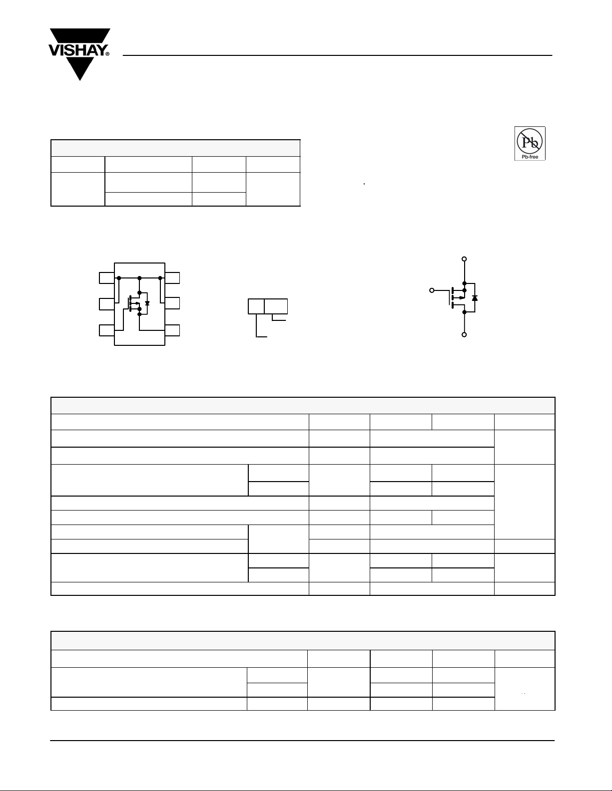
SC-70 (6-LEADS)
1
D
2
D
3
G
SOT-363
DS(on)
Top View
(W) I
New Product
P-Channel 150-V (D-S) MOSFET
FEATURES
D TrenchFETr Power MOSFETS
(A) Qg (T yp)
D
−0.52
D
6
5
D
S
4
Ordering Information: Si1411DH-T1—E3
4.2 nC
Marking Code
BG XX
Part # Code
YY
D Small, Thermally Enhanced SC-70 Package
D Ultra Low On-Resistance
APPLICATIONS
D Active Clamp Circuits in DC/DC Power
Supplies
Lot Traceability
and Date Code
Vishay Siliconix
S
G
D
P-Channel MOSFET
Product Is
Completely
Pb-free
ABSOLUTE MAXIMUM RATINGS (TA = 25_C UNLESS OTHERWISE NOTED)
Parameter Symbol 5 secs Steady State Unit
Drain-Source Voltage V
Gate-Source Voltage V
a
=
nuous Drain Curren
Pulsed Drain Current I
Continuous Diode Current (Diode Conduction)
Single Pulse Avalanche Current
Single Pluse Avalanch Energy
Maximum Power Dissipation
Operating Junction and Storage Temperature Range TJ, T
_
a
a
TA = 25_C
TA = 85_C
L = 0.1 mH
TA = 25_C
TA = 85_C
DM
I
I
AS
E
P
DS
GS
AS
D
S
D
stg
−0.52
−0.38 −0.3
−1.3 −0.83
1.56 1.0
0.81 0.52
−150
"20
−0.8
−2.1
0.22 mJ
−55 to 150 _C
THERMAL RESISTANCE RATINGS
Parameter Symbol Typical Maximum Unit
Maximum Junction-to-Ambient
Maximum Junction-to-Foot (Drain) Steady State R
Notes
a. Surface Mounted on 1” x 1” FR4 Board.
a
t v 5 sec
Steady State
R
thJA
thJF
60 80
100 125
34 45
V
−0.42
A
W
_C/W
Document Number: 73242
S-50461—Rev. B, 14-Mar-05
www.vishay.com
1
Page 2
Si1411DH
DS
,
GS
,
D
VDD = −75 V, RL = 75 W
g
ns
Vishay Siliconix
New Product
SPECIFICATIONS (TJ = 25_C UNLESS OTHERWISE NOTED)
Parameter Symbol T est Condition Min Typ Max Unit
Static
Gate Threshold Voltage V
Gate-Body Leakage I
Zero Gate Voltage Drain Current I
On-State Drain Current
Drain-Source On-State Resistance
Forward Transconductance
Diode Forward Voltage
Dynamic
b
a
a
a
a
Total Gate Charge Q
Gate-Source Charge Q
Gate-Drain Charge Q
Gate Resistance R
Turn-On Delay Time t
Rise Time t
Turn-Off Delay Time t
Fall Time t
Reverse Recovery Time t
Body Diode Reverse Recovery Charge Q
Notes
a. Pulse test; pulse width v 300 ms, duty cycle v 2%.
b. Guaranteed by design, not subject to production testing.
Stresses beyond those listed under “Absolute Maximum Ratings” may cause permanent damage to the device. These are stress ratings only, and functional operation
of the device at these or any other conditions beyond those indicated in the operational sections of the specifications is not implied. Exposure to absolute maximum rating
GS(th)
GSS
DSS
I
D(on)
r
DS(on)
g
V
d(on)
d(off)
fs
SD
g
gs
gd
g
r
f
rr
rr
conditions for extended periods may affect device reliability.
VDS = VGS, I
VDS = 0 V, VGS = "20 V
= −100 mA −2.5 −4.5 V
D
"100 nA
VDS = −150 V, VGS = 0 V −1
VDS = −150 V, VGS = 0 V, TJ = 85_C −5
VDS = −15 V, VGS = −10 V −0.8 A
VGS = −10 V, ID = −0.5 A 2.05 2.6
VGS = −6 V, ID = −0.5 A 2.14 2.7
VDS = −10 V, ID = −0.5 A 1.5 S
IS = −1.4 A, VGS = 0 V −0.80 −1.1 V
4.2 6.3
V
= −75 V, VGS = −10 V, ID = −0.5 A 0.9 nC
DS
1.3
f = 1.0 MHz 8.5 W
4.5 7
VDD = −75 V, RL = 75 W
ID ^ −1 A, V
GEN
= −4.5 V, Rg = 6 W
11 17
9 14
11 17
IF = −0.5 A, di/dt = 100 A/ms
36 55
65 100 nC
mA
W
ns
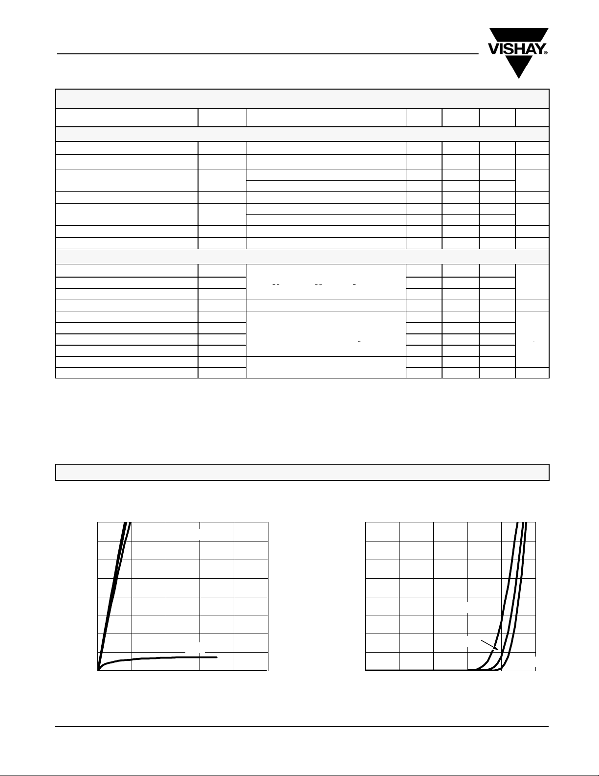
TYPICAL CHARACTERISTICS (25_C UNLESS NOTED)
0.8
0.7
VGS = 10 thru 5 V
0.6
0.5
0.4
0.3
− Drain Current (A)I
D
0.2
0.1
4 V
3 V
0.0
0246810
VDS − Drain-to-Source Voltage (V)
www.vishay.com
2
Output Characteristics Transfer Characteristics
0.8
0.7
0.6
0.5
0.4
0.3
− Drain Current (A)I
D
0.2
TC = 125_C
25_C
0.1
0.0
012345
VGS − Gate-to-Source Voltage (V)
Document Number: 73242
S-50461—Rev. B, 14-Mar-05
−55_C
Page 3
Si1411DH
New Product
TYPICAL CHARACTERISTICS (25_C UNLESS NOTED)
On-Resistance vs. Drain Current
VGS = 6 V
VGS = 10 V
ID − Drain Current (A)
Gate Charge
VDS = 75 V
I
= 0.5 A
D
C − Capacitance (pF)
W )
− On-Resistance (r
DS(on)
4.0
3.5
3.0
2.5
2.0
1.5
1.0
0.5
0.0
0.0 0.1 0.2 0.3 0.4 0.5 0.6 0.7 0.8
10
8
Vishay Siliconix
250
200
150
100
50
C
rss
0
0 30 60 90 120 150
V
On-Resistance vs. Junction Temperature
2.5
VGS = 10 V
I
= 0.5 A
2.0
D
Capacitance
C
iss
C
oss
− Drain-to-Source Voltage (V)
DS
− Gate-to-Source Voltage (V)
GS
V
0.1
− Source Current (A)I
S
6
4
2
0
0.0 0.6 1.2 1.8 2.4 3.0 3.6 4.2
Qg − Total Gate Charge (nC)
Source-Drain Diode Forward Voltage On-Resistance vs. Gate-to-Source Voltage
2
1
TJ = 150_C
TJ = 25_C
1.5
1.0
− On-Resiistance
(Normalized)
DS(on)
r
0.5
0.0
−50 −25 0 25 50 75 100 125 150
6
5
W )
4
3
− On-Resistance (r
2
DS(on)
1
T
− Junction Temperature (_C)
J
ID = 0.5 A
0.01
0 0.3 0.6 0.9
VSD − Source-to-Drain Voltage (V) VGS − Gate-to-Source Voltage (V)
Document Number: 73242
S-50461—Rev. B, 14-Mar-05
1.2 1.5
0
0246810
www.vishay.com
3
Page 4

Si1411DH
Vishay Siliconix
New Product
TYPICAL CHARACTERISTICS (25_C UNLESS NOTED)
Threshold Voltage
1.3
1.0
0.7
0.4
Variance (V)V
GS(th)
0.1
−0.2
−0.5
−50 −25 0 25 50 75 100 125 150
ID = 250 mA
TJ − Temperature (_C)
1
* Limited by
r
DS(on)
0.1
Power (W)
Safe Operating Area
Single Pulse Power, Junction-to-Ambient
35
28
21
14
7
0
10 ms
100 ms
1 ms
10 ms
TA = 25_C
Single Pulse
0.1 1010.010.001
Time (sec)
2
1
0.1
Thermal Impedance
Normalized Effective Transient
0.01
10
Duty Cycle = 0.5
0.2
0.1
0.05
0.02
−4
10
− Drain Current (A)I
0.01
D
TA = 25_C
Single Pulse
0.001
DS(on)
100
0.1 10 1000
*V
1
− Drain-to-Source Voltage (V)
V
DS
u minimum VGS at which r
GS
Normalized Thermal Transient Impedance, Junction-to-Ambient
Single Pulse
−3
−2
10
−1
1 10 60010
Square Wave Pulse Duration (sec)
100 ms
1 s, 10 s
100 s, dc
is specified
Notes:
P
DM
t
1
t
1. Duty Cycle, D =
2. Per Unit Base = R
3. TJM − TA = PDMZ
4. Surface Mounted
2
thJA
t
t
thJA
100
1
2
= 100_C/W
(t)
www.vishay.com
4
Document Number: 73242
S-50461—Rev. B, 14-Mar-05
Page 5

Si1411DH
New Product
TYPICAL CHARACTERISTICS (25_C UNLESS NOTED)
Normalized Thermal Transient Impedance, Junction-to-Foot
2
1
Duty Cycle = 0.5
0.2
0.1
0.1
0.01
0.05
0.02
Single Pulse
−4
10
−3
10
−2
10
Square Wave Pulse Duration (sec)
Thermal Impedance
Normalized Effective Transient
Vishay Siliconix
−1
11010
Vishay Siliconix maintains worldwide manuf ac t ur ing capability. Produc ts m ay be manufac tured at one of several qualified locations. Reliability data f or Silicon Technology and
Package Reliability represent a composite of all qualified locations. For related documents such as package/tape drawings, part marking, and reliability data, see
http://www.vishay.com/ppg?73242.
Document Number: 73242
S-50461—Rev. B, 14-Mar-05
www.vishay.com
5
Page 6

Legal Disclaimer Notice
Vishay
Notice
Specifications of the products displayed herein are subject to change without notice. Vishay Intertechnology, Inc.,
or anyone on its behalf, assumes no responsibility or liability for any errors or inaccuracies.
Information contained herein is intended to provide a product description only. No license, express or implied, by
estoppel or otherwise, to any intellectual property rights is granted by this document. Except as provided in Vishay's
terms and conditions of sale for such products, Vishay assumes no liability whatsoever, and disclaims any express
or implied warranty, relating to sale and/or use of Vishay products including liability or warranties relating to fitness
for a particular purpose, merchantability, or infringement of any patent, copyright, or other intellectual property right.
The products shown herein are not designed for use in medical, life-saving, or life-sustaining applications.
Customers using or selling these products for use in such applications do so at their own risk and agree to fully
indemnify Vishay for any damages resulting from such improper use or sale.
Document Number: 91000 www.vishay.com
Revision: 08-Apr-05 1
Page 7

 Loading...