

Datasheet SG55451BL, SG55451BL-883B, SG55451BY, SG55451BY-883B, SG75451BY Datasheet (Microsemi Corporation)
...Page 1
SG55451B/SG55461/SG55471
SG75451B/SG75461/SG75471
DUAL PERIPHERAL POSITIVE-AND DRIVER
DESCRIPTION
The SG5541B/SG55461/SG55471 (SG75451B/SG75461/SG75471) series of dual peripheral Positive-AND drivers are a family of versatile
devices designed for use in systems that employ TTL or DTL logic. This
family of drivers are direct replacements for the Texas Instruments
SN55451B/61/71 (SN75451B/61/71)series. Diode-clamped inputs simplify circuit design. Typical applications include high-speed logic buffers,
power drivers, relay drivers, MOS drivers, line drivers, and memory drivers.
The SG55451B/SG55461/SG55471 drivers are characterized for operation over the full military ambient temperature range of -55°C to 125°C and
the SG75451B/SG75461/SG75471 drivers are chracterized for operation
from 0°C to 70°C.
FEATURES
••
• 300mA output current capability
••
••
• High-voltage output
••
••
• No output latch-up at 20V
••
••
• High speed switching
••
••
• TTL or DTL compatible diode-clamped inputs
••
••
• Standard supply voltages
••
HIGH RELIABILITY FEATURES
- SG55451B/SG55461/SG55471
♦♦
♦ Available to MIL-STD-883
♦♦
♦♦
♦ Scheduled for MIL-M-38510 QPL listing
♦♦
♦♦
♦ LMI level "S"processing available
♦♦
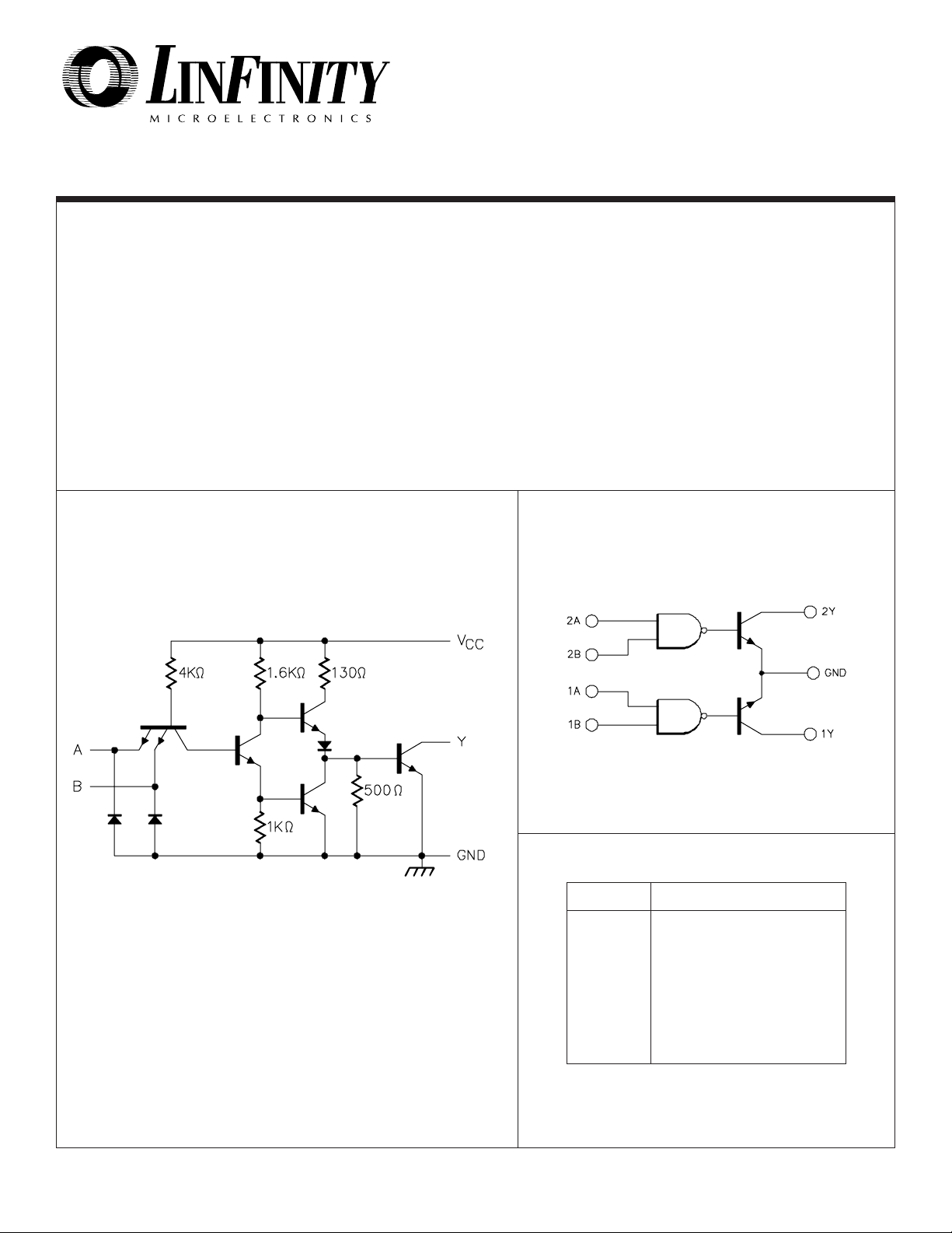
EQUIVALENT CIRCUIT SCHEMATIC (each driver) BLOCK DIAGRAM
Positive Logic: Y = AB
FUNCTION TABLE (each gate)
AB Y
L L L (on-state)
L H L (on-state)
H L L (on-state)
H H H (off-state)
H = High Level, L = Low Level
5/92 Rev 1.1 2/94 LINFINITY Microelectronics Inc.
Copyright 1994 11861 Western Avenue
1 (714) 898-8121
∞ ∞
∞ Garden Grove, CA 92841
∞ ∞
∞∞
∞ FAX: (714) 893-2570
∞∞
Page 2
SG55451B/61/71 SERIES
ABSOLUTE MAXIMUM RATINGS (Note 1)
Supply Voltage (VCC) ............................................................
Input Voltage .....................................................................
Interemitter Voltage
...........................................................
5.5V
5.5V
Off-state Output Voltage
X5451B Series ................................................................
X5461 Series ..................................................................
X5471 Series ..................................................................
Note 1. Exceeding these ratings could cause damage to the device.
30V
35V
70V
THERMAL DATA
Y Package:
Thermal ResistanceThermal Resistance-
L Package:
Thermal ResistanceThermal Resistance-
Junction to Case, θ
Junction to Ambient, θ
Junction to Case, θ
Junction to Ambient, θ
JC
JC
.................. 50°C/W
............ 130°C/W
JA
.................. 35°C/W
............ 120°C/W
JA
RECOMMENDED OPERATING CONDITIONS (Notes 2 & 3)
Supply Voltage (V
SG55451B, SG55461, SG55471 .......................
SG75451B, SG75461, SG75471 ...................
Note 2. Range over which device is functional.
Note 3. The substrate (pin 8) must always be at the most-negative device voltage for proper operation.
)
CC
4.5V to 5.5V
4.75V to 5.25V
Output Current .............................................................
7V
Continuous Total Dissipation at (or below)
25°C Free-Air Temperature .....................................
Operating Junction Temperature
Hermetic (Y, L Packages) ..........................................
Storage Temperature Range ..........................
Lead Temperature (1/16 inch from case
for soldering 60 sec.) .................................................
Note A. Junction Temperature Calculation: TJ = TA + (PD x θJA).
Note B. The above numbers for θ
thermal resistance of the package in a standard mounting configuration. The θ
guidelines for the thermal performance of the device/pcboard system. All of the above assume no ambient
airflow.
Operating Ambient Temperature Range
SG55451B, SG55461, SG55471 ...................
SG75451B, SG75461, SG75471 ........................
400mA
800mW
150°C
-65°C to 150°C
300°C
are maximums for the limiting
JC
numbers are meant to be
JA
-55°C to 125°C
0°C to 70°C
ELECTRICAL CHARACTERISTICS
(Unless otherwise specified, these specifications apply over the operating ambient temperatures for SG55451B/461/471 with -55°C ≤ TA ≤ 125°C, and
SG75451B/461/471 with 0°C ≤ TA ≤ 70°C. Typical values are tested at VCC = 5V, and TA = 25°C. Low duty cycle pulse testing techniques are used
which maintains junction and case temperatures equal to the ambient temperature.)
High-level Input Voltage (V
Low-level Input Voltage (V
Input Clamp Voltage (V
High-level Output Current (I
IH
IL
)
IK
Low-level Output Voltage (V
Input Current at Max V
High-level Input Current (I
Low-level Input Current (I
Supply Current, Outputs High
IN
(IIN)
IH
)
IL
)
Supply Current, Outputs Low
)
OH
SG55451B
Test ConditionsParameter Units
SG55461
SG55471
Min. Typ. Max.
)
22
0.8
V
= MIN, IIN = -12mA
CC
)
OL
V
= MIN, VIH = 2V,
CC
V
= 30V SGX5451B
OH
= 35V SGX5461
V
OH
V
= 70V SGX5471
)
OH
= MIN, VIL = 0.8V, IOL = 100mA
V
CC
V
= MIN, VIL = 0.8V, IOL = 300mA
CC
V
= MAX, VIN = 5.5V
CC
= MAX, VIN = 2.4V
V
CC
V
= MAX, VIN = 0.4V
CC
= MAX, VIN = 5V
V
CC
V
= MAX, VIN = 0V
CC
SGX5451B
SGX5461
SGX5471
-1.2
0.25
0.5
-1.0
8
52
56
56
-1.5
300
0.5
0.8
1.0
60
-1.6
11
65
76
76
SG75451B
SG75461
SG75471
Min. Typ. Max.
0.8
-1.5
-1.2
100
0.4
0.25
0.5
0.7
1.0
60
-1.6
-1.0
11
8
65
52
76
56
76
56
V
V
V
µA
V
V
mA
µA
mA
mA
mA
mA
mA
5/92 Rev 1.1 2/94 LINFINITY Microelectronics Inc.
Copyright 1994 11861 Western Avenue
2 (714) 898-8121
∞ ∞
∞ Garden Grove, CA 92841
∞ ∞
∞∞
∞ FAX: (714) 893-2570
∞∞
Page 3

SG55451B/61/71 SERIES
SWITCHING CHARACTERISTICS (V
= 5V, TA = 25°C)
CC
SG55451B
Test ConditionsParameter Units
SG75451B
Min. Typ. Max. Min. Typ. Max. Min. Typ. Max.
Propagation Delay Time, Low-
18
25
to-High Level Output
Propagation Delay Time, High-
to-Low Level Output
Transition Time, Low-to-High
= 200mA, CL = 15pF,
I
C
R
L
≈ 50Ω
18
25
8
5
Output
Transition Time, High-to-Low
12
7
Level Output
High-Level Output Voltage
After Switching
Note 1. These parameters, although guaranteed, are not tested in production.
(Note 1)
I
= 300mA,
C
= 20V SGX5451B
V
S
V
= 30V SGX5461
S
= 55V SGX5471
V
S
VS-6.5
CONNECTION DIAGRAMS & ORDERING INFORMATION (See Notes Below)
Package
8-PIN CERAMIC DIP
Y - PACKAGE
Part No.
SG55451BY/883B -55°C to 125°C
SG55451BY -55°C to 125°C
SG55461Y/883B -55°C to 125°C
SG55461Y -55°C to 125°C
SG55471Y/883B -55°C to 125°C
SG55471Y -55°C to 125°C
SG75451BY 0°C to 70°C
SG75461Y 0°C to 70°C
SG75471Y 0°C to 70°C
Ambient
Temperature Range
SG55461
SG75461
30
110
25
80
8
25
10
25
-10
V
S
Connection Diagram
1A
1B
1Y
GND 2Y
V
1
2
3
4
SG55471
SG75471
-18
S
8
7
6
5
30
25
10
110
8
80
25
25
ns
ns
ns
ns
mV
mV
mV
V
CC
2B
2A
20-PIN CERAMIC
LEADLESS CHIP CARRIER
L- PACKAGE
SG55451BL/883B -55°C to 125°C
SG55451BL -55°C to 125°C
SG55461L/883B -55°C to 125°C
SG55461L -55°C to 125°C
SG55471L/883B -55°C to 125°C
SG55471L -55°C to 125°C
Note1. Contact factory for JAN and DESC product availability.
2. All parts are viewed from the top.
3. Product is also available in flat pack. Consult factory for price and delivery.
1. N.C.
2. 1A
3. N.C.
4. N.C.
5. 1B
6. N.C.
7. 1Y
8. N.C.
9. N.C.
10. GND
4
5
6
7
8
321
9 11121310
20 19
11. N.C.
12. 2Y
13. N.C.
18
14. N.C.
17
15. 2A
16
16. N.C.
15
17. 2B
18. N.C.
14
19. N.C.
20. V
CC
5/92 Rev 1.1 2/94 LINFINITY Microelectronics Inc.
Copyright 1994 11861 Western Avenue
3 (714) 898-8121
∞ ∞
∞ Garden Grove, CA 92841
∞ ∞
∞∞
∞ FAX: (714) 893-2570
∞∞
 Loading...