

Page 1
SE4100L
PointCharger™ GPS Receiver IC
Preliminary Information
Applications
Mobile phone & PDA accessories
Portable navigation
Personal security
Security systems
Asset tracking
Telematics equipment
Features
30 mW power consumption
4x4mm 24 pin LPCC package
Single conversion radio with integrated IF filters
On-chip, Gain switchable LNA
Low LNA noise figure, 1.3dB typ.
On chip crystal oscillator can be powered up
independently
Fully integrated VCO, VCO tank circuit and PLL.
Remote antenna current detection
Ordering Information
Type Package Remark
SE4100L-R 24 Pin LPCC Shipped in
Tape & Reel
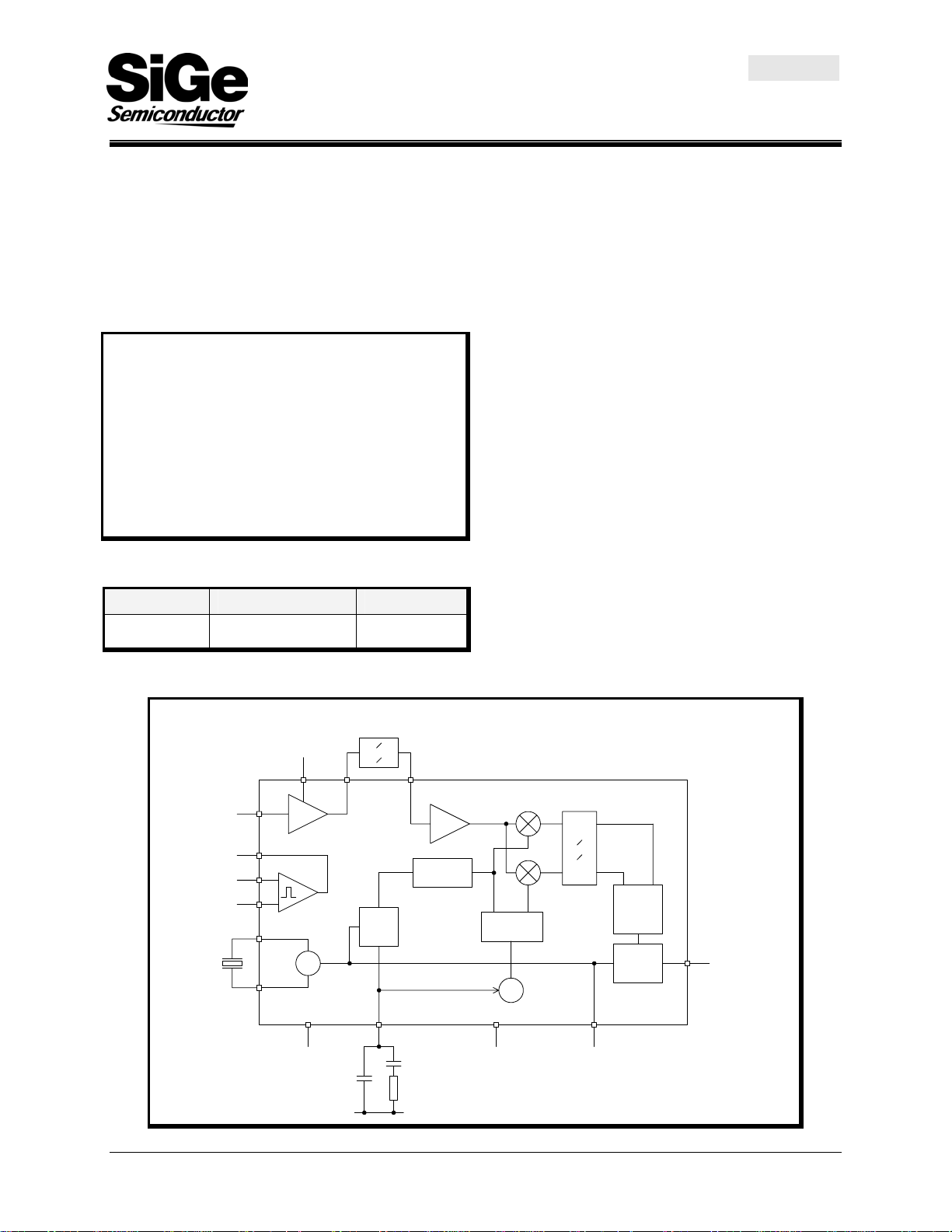
Functional Block Diagram
Product Description
The SE4100 is an integrated GPS receiver designed to
receive the L1 signal at 1575.42MHz. The receiver has
a low IF architecture, and integrates all of the amplifier,
oscillator, mixer and demodulation functions.
The external component count is low, requiring just a
16.368MHz crystal and 11 passive components in its
minimum configuration. This and the 24 pin LPCC
package result in a very small circuit footprint, which is
complemented by just 30mW operating power.
Two digitally controlled shutdown modes enable either
to part to be powered down entirely or for just the 16
MHz clock supply to the baseband processor to be
maintained.
A switchable gain LNA enables the SE4100 to be used
with a local passive antenna or with a remote active
antenna without changing the circuit configuration. The
on-chip VCO and PLL generates the required LO
frequency from the external 16.368MHz crystal. All of
the VCO and LO chain is integrated. An image reject
mixer downconverts the RF signal to a 4.092MHz IF.
The integrated IF filter feeds a combiner, limiter and
output latch. The output signal is a 1-bit quantized
4.092 MHz digital IF at CMOS levels.
SE4100 Block Diagram
~
~
~
Det.
Vtune
MixIn
RF Amp
÷96
IF FilterMixers
IQ
Quadrature
÷2
VCO
~
RxEnb
~
~
~
Phase
Shift /
Combiner
ClkOut
+45° / -45°
Σ
D
D-type
DataOut
QClk
LNAOut
LowGain
LNAIn
AntOK
AntDetP
AntDetN
Xtal1
LNA
Ant current
monitor
Phase
~
Xtal2
27-DST-01 Rev 1.3 Aug 6/02 1 of 16
Xtal
Oscillator
OscEnb
Page 2
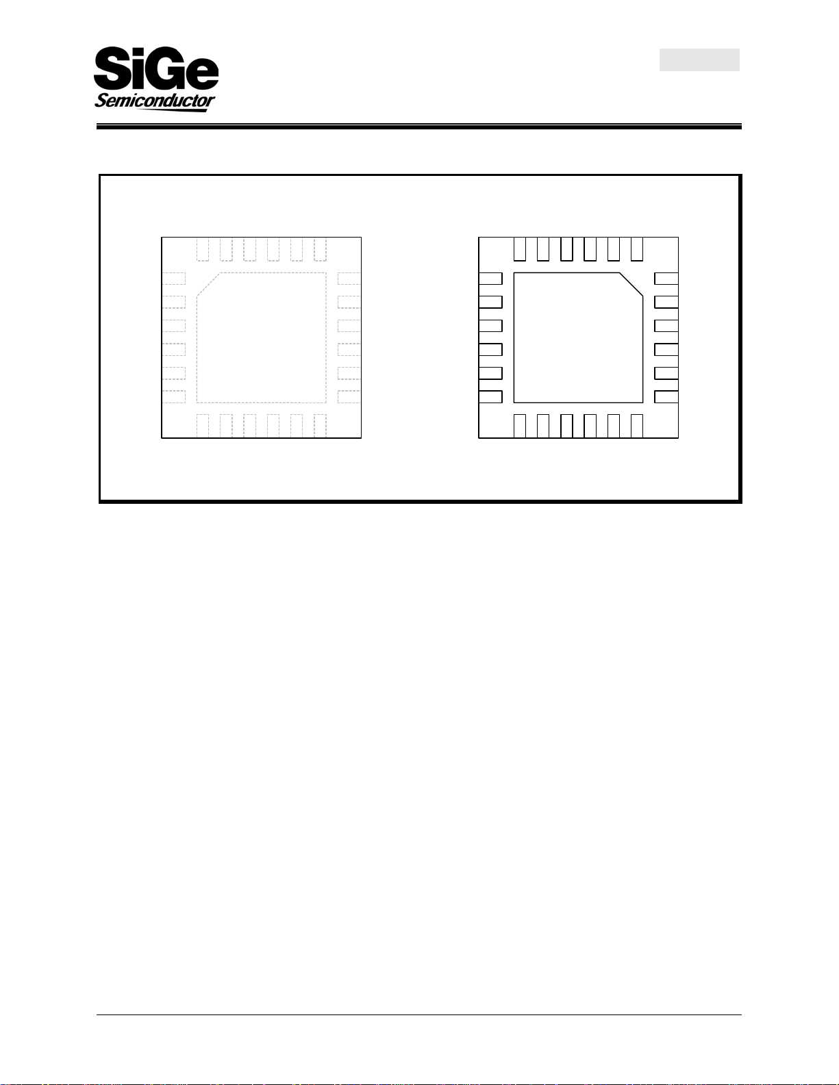
Pin Out Diagram
SE4100L
PointCharger™ GPS Receiver IC
Preliminary Information
VccLNA
AntDetP
AntDetN
LNAIn
LowGain
AntOK
MixIn
Vss2
LNAOut
242123
1
2
3
4
5
6
7108
DataOut
VccRF
22
SE4100L
Top View
9
RxEnb
ClkOut
Vss1
R0
MixIn
20
11
R1
VccVCO
19
12
R2
18
17
16
15
14
13
OscEnb
Vtune
V
DD
Xtal1
Xtal2
R3
OscEnb
Vtune
V
DD
Xtal1
Xtal2
R3
VccVCO
19
18
17
16
15
14
13
12
R2
Vss1
212322
20
SE4100L
Bottom View
10
11
R0
R1
VccRF
Die Pad
9
RxEnb
Vss2
LNAOut
24
VccLNA
1
AntDetP
2
3
AntDetN
4
LNAIn
5
LowGain
6
AntOK
7
8
ClkOut
DataOut
27-DST-01 Rev 1.3 Aug 6/02 2 of 16
Page 3
PointCharger™ GPS Receiver IC
Pin Out Description
Pin No. Name Description
1 VccLNA Power supply connection for LNA
2 AntDetP Connection to battery side of antenna current sensing resistor
3 AntDetN Connection to antenna feed side of antenna current sensing resistor
4 LNAIn LNA Input
5 LowGain LNA Gain control, High = low gain
6 AntOK Antenna OK output flag (high = antenna current OK)
7 DataOut Data Output
8 ClkOut Buffered version of Xtal Osc output / D-type clock
9 RxEnb
10 R0 Reserved internal connection, must be tied to VDD for normal operation
Enable control for Receiver (all circuits except Reference oscillator and Data
Registers), active high input
SE4100L
Preliminary Information
11 R1 Reserved internal connection, must be tied to VDD for normal operation
12 R2 Reserved internal connection, must be tied to VDD for normal operation
13 R3 Reserved internal connection, must be tied to VDD for normal operation
14 Xtal2 Connection to crystal
15 Xtal1 Connection to crystal
16 VDD Power supply for digital circuits (Xtal Oscillator, Data Registers and Bias circuits)
17 Vtune Charge pump output / VCO control voltage input
18 OscEnb Enable control for Reference oscillator, active high input
19 VCCVCO Decoupling connection for VCO power supply
20 MixIn
21 VSS1 Ground
22 VCCRF Power supply connection for all RF circuits except the LNA
23 VSS2 Ground
24 LNAOut
Die Pad Gnd Ground connection for all circuits via die pad
Mixer input signal, 50Ω single ended
LNA Output, 50Ω single ended
27-DST-01 Rev 1.3 Aug 6/02 3 of 16
Page 4
SE4100L
PointCharger™ GPS Receiver IC
Preliminary Information
Functional Description
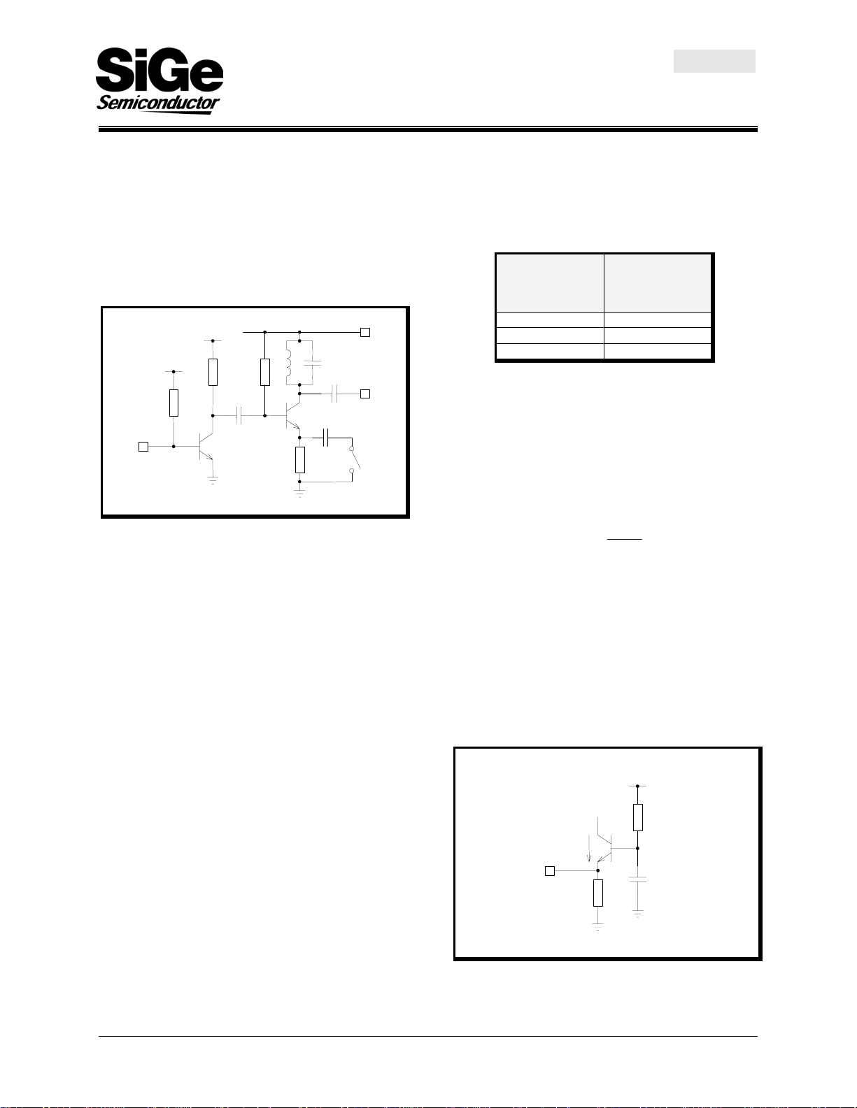
LNA
The internal LNA consists of two transistors
cascaded. The biasing, gain switching circuit and
output matching to 50Ω is contained on the IC. A
conceptual diagram of the internal circuit is shown
below.
Vbias2
Vbias1
LNAIn
The input match to 50Ω requires three external
components, two capacitors and an inductor. The
inductor should be a high Q type, e.g. wirewound or
microstrip; otherwise the low noise figure of the LNA
will not be obtained.
The output match is optimized to allow for a short
length of narrow track between the IC package and a
filter. Exact lengths and track widths will depend on
the board material and thickness.
The gain of the amplifier is switched between high
and low settings by the CMOS level compatible
LowGain input pin. Internally, this reduces the gain of
the second stage only in the low gain setting, which
maintains a low noise figure for the amplifier.
The power supply for the amplifier is provided through
the VccLNA pin. Care should be taken with the PCB
layout to ensure that the power supply cannot act as a
bypass around any filter between the LNA output and
the mixer input.
Antenna Current Monitor
VccLNA
LNAOut
Gain
Control
The state of the logic output on the AntOK pin is
dependent on the voltage drop between AntDetP and
AntDetN pins, AntDetP being the higher dc voltage.
The current setting this voltage is adjusted by
changing the value of the external current sense
resistor between these pins.
Voltage
between
Logic Output
AntOK
AntDetP and
AntDetN (∆V
ANT
)
<0.125 Low
0.25>∆V>0.5
High
>0.75 Low
The AntOK pin is a CMOS output designed to
interface directly to the LowGain input pin, so that in
the event the supply to the external active antenna is
either shorted or open circuited, the internal LNA gain
is switched to the high gain setting.
The external current sense resistor should be chosen
according to the typical current of the external
antenna I
, using the formula:
ANT
0.375
R =
EXT
I
ANT
Mixer RF Input
The mixer RF input pin, MixIn, is a single ended 50Ω
input, designed to either interface to the LNAOut pin
or to the output of an external filter using only a dc
blocking capacitor, and without additional matching
components.
The input is a common base configuration providing a
wideband 50Ω termination. A conceptual diagram of
the input circuit is shown below:
Vbias1
0.5mA
MixIn
Ω
800
The antenna current monitor is a window comparator
designed to operate with common mode input
voltages above the chip V
the supply current to an external active antenna and
provide a logic output indicating if the current is within
. It is designed to monitor
CC
the desired range.
27-DST-01 Rev 1.3 Aug 6/02 4 of 16
Page 5
SE4100L
PointCharger™ GPS Receiver IC
Preliminary Information
The filter type chosen should require a termination
impedance of 50+j0Ω. Examples of suitable types are
shown on the application schematic diagram.
The PCB layout should keep the track from the filter
to the MixIn pin as short as possible to minimize
pickup and mismatch (if the track is not 50Ω). A dc
blocking capacitor should be used, even if the filter
does not present a dc path, as the MixIn pin has 0.4V
dc present which may be detrimental to the filter.
A filter will improve the performance of the receiver in
the presence of out of band blocking signals, but is
not essential if operation in the presence of such
signals is not critical. If the filter is not fitted, the
LNAOut pin should be connected to the MixIn pin via
a coupling capacitor.
PLL and Loop Filter
The entire phase-locked loop generating the local
oscillator for the mixer is contained on-chip, with the
exception of the loop filter.
Values provided on the application circuit should be
used, as these will provide optimum performance
under all conditions.
The capacitors may be ceramic dielectric types, with
either COG/NP0 or X7R dielectric. Higher
capacitance per unit volume dielectrics should be
avoided as the absolute tolerance and temperature
stability may compromise system performance.
The PCB layout should keep the track from the Vtune
pin to the loop filter as short as possible to minimize
noise pickup.
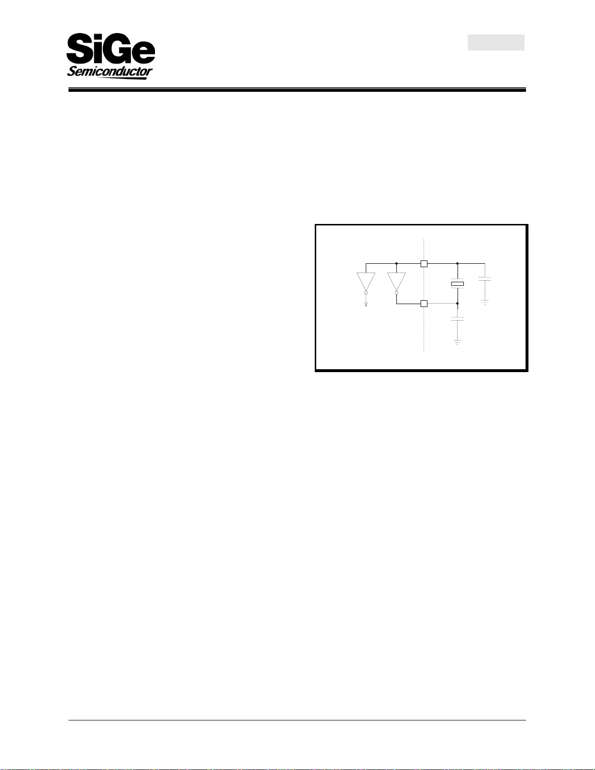
Crystal Oscillator
The crystal oscillator is a Pierce configuration, as
shown in the diagram below. The application circuit is
designed to work with parallel resonant crystals with a
load capacitance of 12pF.
Xtal1
Xtal2
The PCB layout should minimize the lengths of the
tracks to Xtal1 and Xtal2 pins. The capacitors at each
terminal of the crystal should be mounted adjacent to
the crystal and have a low impedance connection to
the ground plane.
27-DST-01 Rev 1.3 Aug 6/02 5 of 16
Page 6

SE4100L
PointCharger™ GPS Receiver IC
Preliminary Information
Absolute Maximum Ratings
These are stress ratings only. Exposure to stresses beyond these maximum ratings may cause permanent damage
to, or affect the reliability of the device. Avoid operating the device outside the recommended operating conditions
defined below.
This device is ESD sensitive. Handling and assembly of this device should be at ESD protected workstations.
Symbol Parameter Min. Max. Unit
VCC, VDD Supply Voltage -0.3 +4.6 V
Voltage On Any Pin With Respect To V
AntDetP and AntDetN Pins
Voltage On AntDetP and AntDetN Pins With
,
Respect To VSS
Storage Temperature Range -65 +150
V
AntDetP
V
AntDetN
T
STG
except
SS
-0.3 V
+0.3 V
DD
-0.3 +6.0 V
°C
Recommended Operating Conditions
Symbol Parameter Min. Typ. Max. Unit
TA Operating Temperature -40 +25 +85
°C
VCC, VDD Supply Voltage 2.7 3.6 V
DC Electrical Characteristics
Symbol Parameter Min. Typ. Max. Unit
ICC Total Supply Current, All Circuits Active 9 mA
I
Supply Current, Oscillator Only Active 1.0 mA
CC(OSC)
I
Supply Current, No Circuits Active 10
CC(OFF)
µA
27-DST-01 Rev 1.3 Aug 6/02 6 of 16
Page 7

SE4100L
PointCharger™ GPS Receiver IC
Preliminary Information
AC Electrical Characteristics
LNA
Symbol Parameter Note Min. Typ. Max. Unit
V
LNA Supply Voltage 2.7 3.6 V
CCLNA
ICC Supply Current , RxEnb = ‘1’ 1.2 mA
S21
S21
Z11
NF
LOW
NF
Forward Gain, f
LowGain = ‘0’, P
Noise Figure, f
LowGain = ‘0’
Forward Gain, f
LowGain = ‘1’, P
Noise Figure, f
LowGain = ‘1’
Input Impedance, Single Ended Input, With
External Matching Circuit
=1570MHz to 1580MHz,
RF
= -80dBm
in
=1570MHz to 1580MHz,
RF
=1570MHz to 1580MHz,
RF
= -80dBm
in
=1570MHz to 1580MHz,
RF
20 dB
1.3 dB
7 dB
2.5 4 dB
30-j75
Ω
S22
IIP3H
IIP3L
Output Return Loss, 50Ω system, Single
Ended Output
High Gain Mode Input IP3, Tones At 1575 ±
5MHz @ –60dBm
Low Gain Mode Input IP3, Tones At 1575 ±
5MHz @ –60dBm
-10 dB
-25 dBm
-15 dBm
P1dB Input Power At Which Gain Falls By 1dBm -34 dBm
tR
Recovery Time From –3dBm Input Overload
Signal
4 10
VIL Input Low Level, LowGain Input 0.6 V
VIH Input High Level, LowGain Input VDD-0.6 V
IIN LowGain Input Current -0.1 0.1
µsec
µA
27-DST-01 Rev 1.3 Aug 6/02 7 of 16
Page 8

SE4100L
PointCharger™ GPS Receiver IC
Preliminary Information
Receiver
Symbol Parameter Note Min. Typ. Max. Unit
ICC Supply Current , RxEnb = ‘1’ 8.0 mA
NF
Noise Figure, f
Input to ‘MixIn’
=1570MHz To 1580MHz,
RF
10 dB
IIP3
S11
tR
Input IP3, Tones 1575 ± 5MHz @ -40dBm
(Mixer and IF Filter Only)
Input Return Loss, 50Ω System
Recovery Time From –30dBm Input
Overload Signal
-15 dBm
-10 dB
4 10
µsec
fIF IF Centre Frequency 4.092 MHz
BW -3dB Bandwidth 2.0 MHz
∆T
Group Delay Variation, f
g
Av2
Av4
Attenuation At f
Attenuation At f
± BW
C
± 2.BW
C
± BW/2
C
0.1
µsec
11 dB
27 dB
VCO and Local Oscillator
Symbol Parameter Note Min. Typ. Max. Unit
f
VCO Centre frequency
VCO
3142.656
MHz
L1k LO SSB Phase noise at 1kHz offset -65 dBc/Hz
L
LO SSB Phase noise at 10kHz offset -65 dBc/Hz
10k
L
LO SSB Phase noise at 100kHz offset -85 dBc/Hz
100k
Crystal Oscillator
Symbol Parameter Note Min. Typ. Max. Unit
ICC
f
XTAL
Supply Current, Crystal Oscillator And Clock
Buffers, OscEnb = ‘1’
1.0 mA
Oscillator Frequency 16.368 MHz
Crystal Parameters
Mode
Parallel
fund.
Frequency 16.368 MHz
ESR 50
C
12 pF
LOAD
Ω
Oscillator Startup Time To 95% Of Final
t
START
Amplitude And Within 10ppm Of Final
100
µsec
Frequency
27-DST-01 Rev 1.3 Aug 6/02 8 of 16
Page 9

SE4100L
PointCharger™ GPS Receiver IC
Preliminary Information
Antenna Current Monitor
Symbol Parameter Note Min. Typ. Max. Unit
∆V
∆V
∆V
V
AntDetP
V
V
ANT
ANT
ANT
AntOK
AntOK
Voltage Between AntDetP And AntDetN For
AntOK = High
Voltage Between AntDetP And AntDetN For
AntOK = Low For Low Current Condition
Voltage Between AntDetP And AntDetN For
AntOK = Low For High Current Condition
Voltage Range On AntDetP For Normal
Operation
AntOK Output Voltage, Antenna OK, 1mA
Current Source
AntOK Output Voltage, Antenna Not OK,
1mA Current Sink
0.25 0.5 V
0.125 V
0.75 V
Vcc-0.5 5.25 V
Vcc-0.5 Vcc V
0 0.5 V
27-DST-01 Rev 1.3 Aug 6/02 9 of 16
Page 10

SE4100L
PointCharger™ GPS Receiver IC
Preliminary Information
Timing Characteristics
Symbol Parameter Note Min. Typ. Max. Unit
t
Clock Period 60 nsec
PEr
t
Clock Low Width 20 nsec
PWL
t
Clock High Width 20 nsec
PWH
t
Clock To Data Delay Time 5 nsec
DEL
t
Setup Time 21 nsec
SETUP
t
Hold Time 26 31 nsec
HOLD
tR Rise Time, 10-90% 8 nsec
t
Rise and Fall Time, 10-90% 8 nsec
R/F
Output Data Timing Diagram
t
= 60ns min t
PER
= 20ns min
PWH
CLKOut
t
= 20ns min
PWL
t
SETUP
= 21ns min
t
= 31ns max, 26ns min
HOLD
t
R(10-90%)
= 8ns max
t
= 5ns max
DEL
DataOut
t
R/F(10-90%)
= 8ns max
27-DST-01 Rev 1.3 Aug 6/02 10 of 16
Page 11

Figure 1: Typical Schematic Diagram
SE4100L
PointCharger™ GPS Receiver IC
Preliminary Information
C11
9pF
1575.42MHz Filter
eg. Sawtek 855969 or Murata SAFCC1G57AA0S00
~~~
C4
22p
C5
100p
R1
C6
18
19
MixIn
20
Vss1
21
VccRF
Vss2
23
24
1
C7
6.8K
580pF
17
OscEnb
VccVCO
LNAOut
VccLNA
2
Vtune
AntDetP
16
3
120pF
DD
V
IC1
AntDetN
X1
C10
22pF
14
15
Xtal1
13
R3
a
p
Xtal2
e
i
D
SE4100
LowGain
LNAIn
4
AntOK
6
5
16.368MHz
1n
C8
C9
d
R2
12
R1
11
R0
10
RxEnb
922
ClkOut
8
DataOut
7
10n
R2
C12
10n
C13
39Ω
22p
C1
L2 47nH 10%
L1
TBD
10%
C2
1p
22p
C3
100p
Vcc
RxEnb
+5V (Antenna
Antenna
DataOut
ClkOut
LNA Supply)
OscEnb
27-DST-01 Rev 1.3 Aug 6/02 11 of 16
Page 12

PointCharger™ GPS Receiver IC
Preliminary Information
Figure 2: Minimum Component Count Application Schematic Diagram
C11
9pF
X1
C10
22pF
14
13
R3
e
Xtal2
i
D
16.368MHz
d
a
p
R2
12
R1
11
R0
10
RxEnb
922
ClkOut
8
DataOut
7
C5
100p
C8
C4
C7
R1
6.8k
120pF
C6
580pF
1n
15
16
17
18
DD
V
Vtune
OscEnb
19
20
21
VccVCO
MixIn
Vss1
VccRF
Xtal1
IC1
SE4100
Vss2
23
10p
24
LNAOut
C9
SE4100L
10n
C1
LowGain
5
TBD
C2
22p
AntOK
6
10%
1p
LNAIn
4
L1
C3
100p
VccLNA
AntDetP
AntDetN
1
3
2
Vcc
Antenna
DataOut
ClkOut
OscEnb
RxEnb
27-DST-01 Rev 1.3 Aug 6/02 12 of 16
Page 13

C
a
C
a
PointCharger™ GPS Receiver IC
Typical PCB Layout (With Filter And Antenna Current Sensing)
Total size of layout = 15.5 x 10.5mm
15.5mm
VCC
Antenna
VCC
Antenna
C12
C13
R2
L2
F1
C5
C3
SiGe
C1
C2
SE4100
L1
Data Out
Clock Out
Rx Enable
R1
C7
C4
C6
C8
C9
Osc Enable
C11
10.5mm
X1
C10
Typical PCB Layout (Minimum Component Count)
Total size of layout = 12.5 x 9.0mm
12.5mm
SE4100L
Preliminary Information
R1
C12 C13
R2
L2
C1
C2
C11
F1
C7
C4
C5
C6
C8
X1
C3
SiGe
SE4100
L1
C10
C9
Actual size
VCC
Antenna
C9
C6
C2
C3
C1
L1
C4
C5
SiGe
R1
C7
C8
C11
X1
9.0mm
SE4100
C10
Data Out
Clock Out
Rx Enable
Osc Enable
C11
C9
C6
R1
C4
C2
C3
C5
C7
X1
C1
SiGe
L1
C8
SE4100
C10
Actual size
(R2, C12, C13, L2, F1 not used)
Note: These layouts are for illustration purposes only. Reference designs and layout
information are available from SiGe Semiconductor.
27-DST-01 Rev 1.3 Aug 6/02 13 of 16
Page 14

Typical Bill Of Materials for Application PCB Layout
Component Value Type Manufacturer
IC1 SE4100 SiGe
C1 22pF 0402 ceramic
C2 1pF 0402 ceramic
C3 100pF 0402 ceramic
C4 22pF 0402 ceramic
C5 100pF 0402 ceramic
C6 580pF 0402 ceramic
C7 120pF 0402 ceramic
C8 1nF 0402 ceramic
C9 10nF 0402 ceramic
SE4100L
PointCharger™ GPS Receiver IC
Preliminary Information
C10 22pF 0402 ceramic
C11 9pF 0402 ceramic
C12 10nF 0402 ceramic
C13 22pf 0402 ceramic
L1 TBD 10% 0402CS-??NXJ Coilcraft
L2 47nH, 10% 0402CS-47NXK Coilcraft
R1
R2
F1 1575.42MHz 855969 Sawtek
X1 16.368MHz KSX series AVX
6.8kΩ
39Ω
0402
0402
27-DST-01 Rev 1.3 Aug 6/02 14 of 16
Page 15

Package Information
SE4100L
PointCharger™ GPS Receiver IC
Preliminary Information
27-DST-01 Rev 1.3 Aug 6/02 15 of 16
Page 16

SE4100L
PointCharger™ GPS Receiver IC
Preliminary Information
http://www.sige.com
Headquarters: Canada
Phone: +1 613 820 9244
Fax: +1 613 820 4933
2680 Queensview Drive
Ottawa ON K2B 8J9 Canada
sales@sige.com
San Diego United Kingdom
Phone: +1 858 668 3541 South Building, Walden Court
Fax: +1 858 668 3546 Parsonage Lane, Bishop’s Stortford
Hertfordshire CM23 5DB
Hong Kong
Phone: +44 1279 464 200
Phone: +1 852 9177 1917 Fax: +44 1279 464 201
Product Preview
The datasheet contains information from the product concept specification. SiGe Semiconductor Inc. reserves the right to change
information at any time without notification.
Preliminary Information
The datasheet contains information from the design target specification. SiGe Semiconductor Inc. reserves the right to change
information at any time without notification.
Final
The datasheet contains information from the final product specification. SiGe Semiconductor Inc. reserves the right to change
information at any time without notification. Production testing may not include testing of all parameters.
Information furnished is believed to be accurate and reliable and is provided on an “as is” basis. SiGe Semiconductor Inc. assumes
no responsibility or liability for the direct or indirect consequences of use of such information nor for any infringement of patents or
other rights of third parties, which may result from its use. No license or indemnity is granted by implication or otherwise under any
patent or other intellectual property rights of SiGe Semiconductor Inc. or third parties. Specifications mentioned in this publication
are subject to change without notice. This publication supersedes and replaces all information previously supplied. SiGe
Semiconductor Inc. products are NOT authorized for use in implantation or life support applications or systems without express
written approval from SiGe Semiconductor Inc.
RangerChargerTM, StreamChargerTM, PointChargerTM, and LightChargerTM are trademarks owned by SiGe Semiconductor Inc.
Copyright 2002 SiGe Semiconductor
All Rights Reserved
27-DST-01 Rev 1.3 Aug 6/02 16 of 16
 Loading...