

Page 1
SCANPSC100F
Embedded Boundary Scan Controller
(IEEE 1149.1 Support)
General Description
The SCANPSC100F is designed to interface a generic parallel processor bus to a serial scan test bus. It is useful in improving scan throughput when applying serial vectors to system test circuitry and reduces the software overhead that is
associated with applying serial patterns with a parallel processor. The ’PSC100F operates by serializing data from the
parallel bus for shifting through the chain of 1149.1compliant
components (i.e., scan chain). Scan data returning from the
scan chain is placed on the parallel port to be read by the
host processor. Up to two scan chains can be directly controlled with the ’PSC100F via two independent TMS pins.
Scan control is supplied with user specific patterns which
makes the ’PSC100F protocol-independent. Overflow and
underflow conditions are prevented by stopping the test
clock.A32-bit counter is used to program the number of TCK
cycles required to complete a scan operation within the
boundary scan chain or to complete a ’PSC100F Built-In Self
Test (BIST) operation. SCANPSC100F device drivers and
1149.1 embedded test application code are available with
National’s SCANEase software tools.
Features
n Compatible with IEEE Std. 1149.1 (JTAG) Test Access
Port and Boundary Scan Architecture
n Supported by National’s SCAN Ease (Embedded
Application Software Enabler) Software
n Uses generic, asynchronous processor interface;
compatible with a wide range of processors and PCLK
frequencies
n Directly supports up to two 1149.1 scan chains
n 16-bit Serial Signature Compaction (SSC) at the Test
Data In (TDI) port
n Automatically produces pseudo-random patterns at the
Test Data Out (TDO) port
n Fabricated on FACT
™
1.5 µm CMOS process
n Supports 1149.1 test clock (TCK) frequencies up to
25 MHz
n TTL-compatible inputs; full-swing CMOS outputs with
24 mA source/sink capability
n Standard Microcircuit Drawing (SMD) 5962-9475001
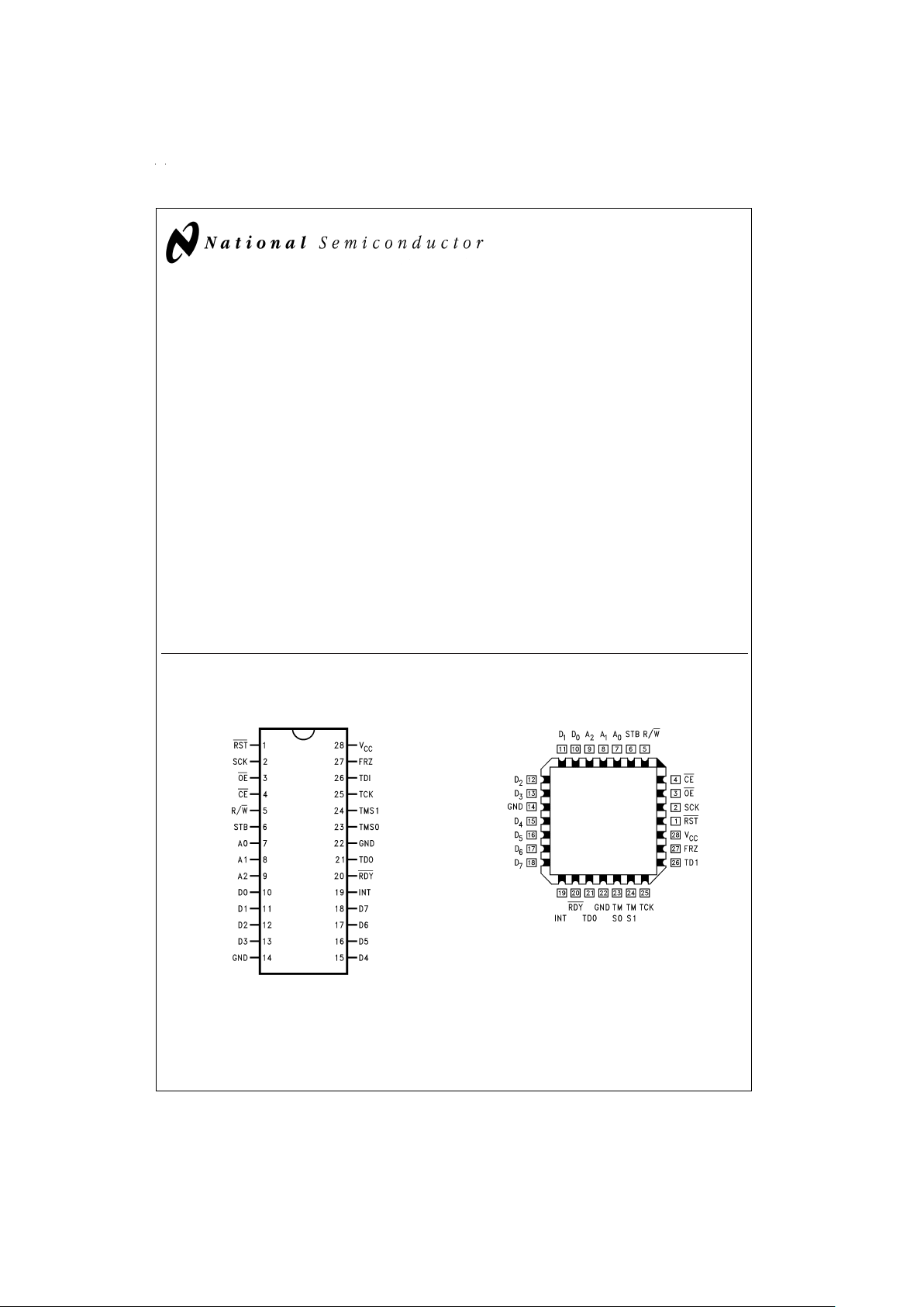
Connection Diagrams
FACT™is a trademark of Fairchild Semiconductor Corporation.
TRI-STATE
®
is a registered trademark of National Semiconductor Corporation.
28-Pin DIP and Flatpak
DS100325-1
Pin Assignment for LCC
DS100325-18
September 1998
SCANPSC100F Embedded Boundary Scan Controller (IEEE 1149.1 Support)
© 1999 National Semiconductor Corporation DS100325 www.national.com
Page 2
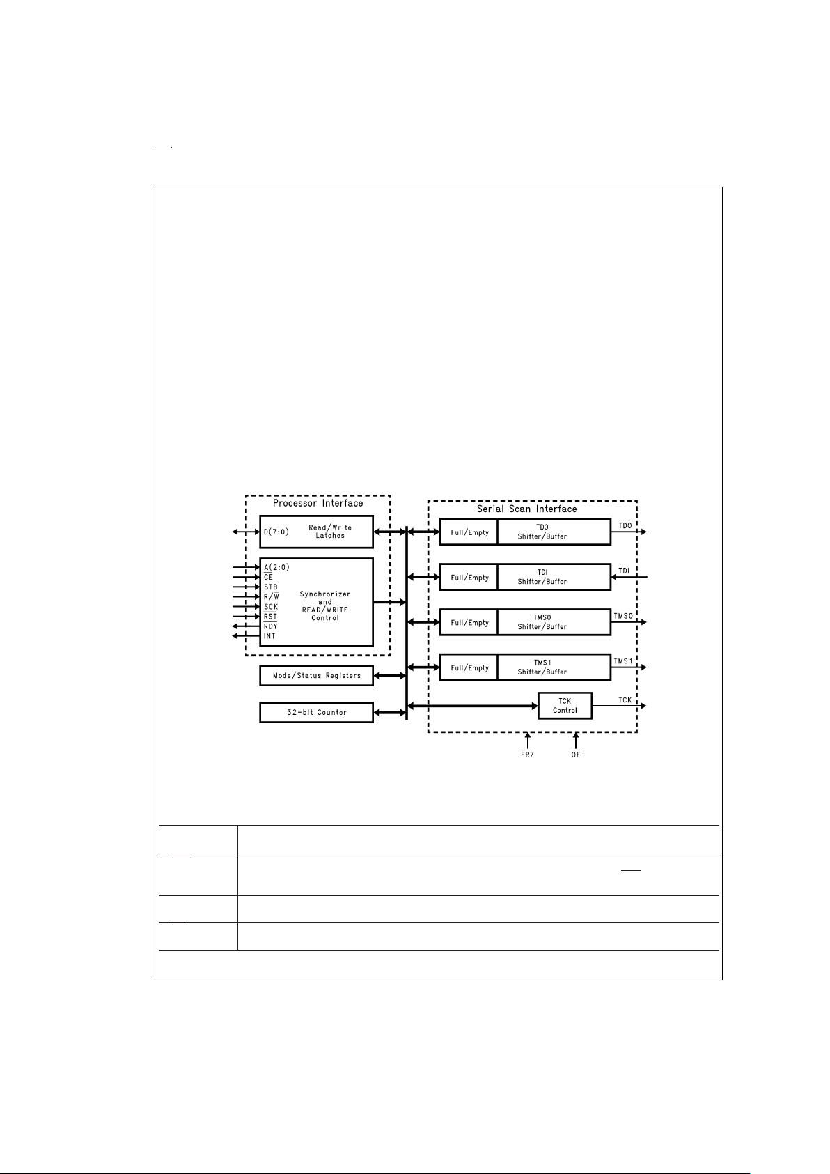
Chip Architecture
The ’PSC100 is designed to act together with a parallel bus
host as a serial test bus master. Parallel data is written by the
host to the ’PSC100, which serializes the data for application
to a serial test bus. Serial data returningfrom thetarget scan
chain(s) is placed on the processor port for parallel reads.
Several features are included in the ’PSC100 which make
scan test communication more convenient and efficient.
Figure 1
shows the major functional blocks of the ’PSC100
design. The Parallel Processor Interface (PPI) is an asynchronous, 8-bit parallel interface which is used by the host
processor to write and read data. The PPI generates the
necessary internal data, address, and control signals to
complete internal write and read operations.
The Serial Scan Interface (SSI) consists of a bank of
double-buffered parallel/serial shift registers (i.e.,a2x8bit
FIFO), or Shifter/Buffers. The double buffering improves efficiency by allowing parallel writes or reads to/from one of the
two 8-bit FIFOs within the shifter/buffer while the other FIFO
is shifting data to/from the scan chain. Three Shifter/Buffers
are provided for outgoing serial data and one for incoming
serial data. TestData Out (TDO) is for scanning out test data
while the two TestMode Select signals (TMS0/1) are used to
provide user specific control data. Test Data In (TDI) receives serial data from the scan chain. A local control block
is associated with each Shifter/Buffer to provide shift and
load control as well as providing full or empty status. The SSI
also provides Test Clock (TCK) Control. TCK is stopped and
started depending on the status of the Shifter/Buffers or the
32-bit Counter. By stopping and starting TCK, scan operations will proceed only when the enabled Shifter/Buffers are
ready to send and/or receive serial data.
The 32-bit Counter (CNT32) is a count-down binary counter
included to assist in controlling the SSI. The initial state of
CNT32 is loaded from the parallel port with four consecutive
writes to its address. When enabled, CNT32 is used to program the number of TCKs applied by the SSI to the boundary scan chain(s). The value of CNT32 can also be used to
generate interrupts (i.e., when CNT32 reaches terminal
count) and to trigger ’PSC100 features, such as, Auto TMS
High (discussed later within this datasheet).
The Mode and Status Registers are used to control and observe the operation of the SSI and CNT32. Each of the
Shifter/Buffers and CNT32 have an associated mode bit
which enables it for participation in on-going operations. Status bits can be used for polling operations.
Pin Descriptions
Pin Description
Name
RST (Input)
The Reset pin is an asynchronous input that, when low, initializes the ’PSC100. Mode bits, Shifter/Buffer
and CNT32 control logic, TCK Control, and the PPI are all initialized to defined states. RST has hysteresis
for improved noise immunity.
SCK (Input) The System Clock drives all internal timing. The test clock, TCK, is a gated and buffered version of SCK.
SCK has hysteresis for improved immunity.
OE (Input)
Output Enable TRI-STATEs all SSI outputs when high. A 20 kΩ pull-up resistor is connected to
automatically TRI-STATE
®
these outputs when this signal is floating.
DS100325-2
FIGURE 1. ’PSC100 Block Diagram
www.national.com 2
Page 3
Pin Descriptions (Continued)
Pin Description
Name
CE (Input)
Chip Enable, when low, enables the PPI for byte transfers. D(7:0) and RDY are TRI-STATEd if CE is high.
CE has hysteresis for improved noise immunity.
R/W (Input) Read/Write defines a PPI cycle —Read when high, Write when low. R/ W has hysteresis for improved
noise immunity.
STB (Input) Strobe is used for timing all PPI byte transfers. D(7:0) are TRI-STATEd when STB is high. All other PPI
inputs must meet specified setup and hold times with respect to this signal. STB has hysteresis for
improved noise immunity.
A(2:0) The Address pins are used to select the register to be written to or read from.
(Input)
D(7:0) (I/O) Bidirectional pins used to transfer parallel data to and from the ’PSC100.
INT Interrupt is used to trigger a host interrupt for any of the defined interrupt events. INT is active high.
(Output)
RDY
Ready is used to synchronize asynchronous byte transfers between the host and the ’PSC100. When low,
(TRI-STATE RDY signals that the addressed register is ready to be accessed RDY is enabled when CE is low.
Output)
TDO Test Data Out is the serial scan output from the ’PSC100. TDO is enabled when OE is low.
(TRI-STATE
Output)
TMS(1:0) The Test Mode Select pins are serial outputs used to supply control logic to the UUT. TMS(1:0) are
(TRI-STATE enabled when OE is low.
Output)
TCK The Test Clock output is a buffered version of SCK for distribution in the UUT. TCK Control logic starts
(TRI-STATE and stops TCK to prevent overflow and underflow conditions. TCK is enabled when OE is low.
Output)
TDI (Input) Test Data In is the serial scan input to the ’PSC100. A 20 kΩ pull-up resistor is connected to force TDI to
a logic 1 when the TDO line from the UUT is floating.
FRZ (Input) The Freeze pin is used to asynchronously generate a user-specific pulse on TCK. If the FRZ Enable Mode
bit is set, TCK will be forced high if FRZ goes high. FRZ has hysteresis for improved noise immunity.
Mode and Status Registers
MODE REGISTER 0 (MODE0)
Bit 7 Bit 6 Bit 5 Bit 4 Bit 3 Bit 2 Bit 1 Bit 0
TDO TDI CNT32 TMS0 TMS1 Auto TMS High Loop-
Enable Enable Enable Enable Enable Reserved Enable Around
Enable
This register is purely a mode register. All bits are writeable
and readable. The value 00100000 is placed in this register
upon RST low or a synchronous reset operation.
•
Bit 7: This bit enables the TDO shifter/buffer for shift op-
erations. If this bit is set, the TDO shifter/buffer will
cause TCK to stop if it is empty.
•
Bit 6: This bit enables the TDI shifter/buffer for shift op-
erations. If this bit is set, the TDI shifter/buffer will
cause TCK to stop if it is full.
•
Bit 5: This bit enables the 32-bit counter. If this bit is set,
the counter will cause TCK to stop if if has not been
loaded or if it has reached terminal count.
•
Bit 4: This bit enables the TMS0 shifter/bufferfor shift op-
erations. If this bit is set, the TMS0 shifter/bufferwill
cause TCK to stop if it is empty.
•
Bit 3: This bit enables the TMS1 shifter/bufferfor shift op-
erations. If this bit is set, the TMS1 shifter/bufferwill
cause TCK to stop if it is empty.
•
Bit 2: This bit is reserved and should remain as a logic 0
during all ’PSC100 operations.
•
Bit 1: If this bit is set, TMS will be forced high when the
32-bit counter is at state (00000001)h.
•
Bit 0: This bit causes TDI to be connected directly back
through TDO for Loop-Around operations.
www.national.com3
Page 4
Mode and Status Registers (Continued)
MODE REGISTER 1 (MODE1)
Bit 7 Bit 6 Bit 5 Bit 4 Bit 3 Bit 2 Bit 1 Bit 0
TDO TDI CNT32 PRPG SSC Freeze Test Test
Interrupt Interrrupt Interrupt Enable Enable Pin Loop- Loop-
Enable Enable Enable Enable Back Back
This register is purely a mode register. All bits are writeable
and readable. The value 00000000 is placed in this register
upon RST low or a synchronous reset operation.
•
Bit 7: If this bit is set and the TDO shifter/buffer is
not full (i.e., one or both 8-bit TDO FIFOs
are empty), the INT pin will go high.
•
Bit 6: If this bit is set and the TDI shifter/buffer is
not empty (i.e., one or both 8-bit TDI FIFOs
are full), the INT pin will go high.
•
Bit 5: If this bit is set, and the 32-bit counter is not
loaded or has reached terminal count, the
INT pin will go high.
•
Bit 4: This bit signifies that the TD0 shifter/buffer
is reconfigured as a 32-Bit Pseudo Random
Pattern Generator. If set, and MODE0 Bit 7
is set, the TDO shifter/buffer will stop TCK
until a seed value has been written to all
four of the 8-bit LFSR segments.
•
Bit 3: This bit signifies that the TD1 shifter/buffer
is reconfigured as a 16-Bit Serial Signature
Compactor. If set, and MODE0 Bit 6 is set,
the TDI shifter/buffer will cause TCK to stop
until a seed value has been written to the
two TDI registers.
•
Bit 2: If this bit is set, a high value on FRZ will
force TCK high (see TCK Control Section).
•
Bits 1 and 0: These bits are used to control
Test Loop-Back operations according to the
following table.
MODE1 MODE1 Function
Bit 1 Bit 0
0 0 Normal Operation
0 1 Loop-Back TDO to TDI
1 0 Loop-Back TMS0 to TDI
1 1 Loop Back TMS1 to TDI
MODE REGISTER 2 (MODE2)
Write:
Bit 7 Bit 6 Bit 5 Bit 4 Bit 3 Bit 2 Bit 1 Bit 0
Not Not Not Not Continuous Update Single
Used Used Used Used Update Status Reset Step
CNT32
Read:
Bit 7 Bit 6 Bit 5 Bit 4 Bit 3 Bit 2 Bit 1 Bit 0
TDO TDI CNT32 TMS0 TMS1 Continuous Single
Status Status Status Status Status Update Reset Step
CNT32
This register contains both mode and status bits. Bits 4–7
are status bits only. Bit 3 is a status bit during read operations and a mode bit during write operations. Bits 0–2 are
mode bits only. Upon RST low, or a synchronous reset, the
value placed in MODE2 is 10111000 (Read mode). Latches
used to update status bits 3–7 retain their last state upon
RST and are in an “unknown” state after power-up. Toinitialize the latches to a known state, they need to be updated using the Update Status bit (bit 2) or continuous update bit (bit
3).
•
Bit 7: Set high if theTDO shifter/buffer is not full, i.e., one
or both 8-bit TDO FIFOs are ready to be written to.
•
Bit 6: Set high if the TDI shifter/buffer is not empty, i.e.,
one or both 8-bit TDI FIFOs are ready to be read
from.
•
Bit 5: Set high if the 32-bit counter has not been loaded,
or has reached terminal count.
•
Bit 4: Set high if the TMS0 shifter/buffer is not full, i.e.,
one or both 8-bit TMS0 FIFOs are ready to be written to.
•
Bit 3 (Read Cycle):
Set high if the TMS1 shifter/buffer is not full, i.e.,
one or both 8-bit TMS1 FIFOs are ready to be written to.
•
Bit 3 (Write Cycle):
If set, will cause all status bits to be continuously
updated.
•
Bit 2 (Read Cycle):
Shows the state of the Continuous Update bit during read operations (Bit 3 during writes).
www.national.com 4
Page 5

Mode and Status Registers (Continued)
•
Bit 2 (Write Cycle):
If set, will cause a pulse to be issued internally that
will update all status bits. This bit will be reset upon
completion of the pulse. The state of this bit is not
readable. It is reset upon RST low.
•
Bit 1: If set, will cause a synchronous reset of all func-
tions except the parallel interface. The value of this
bit will return to zero when the reset operation is
complete.
•
Bit 0: If set, will cause the 32-bit counter to count for one
SCK cycle (no TCK cycle will be generated). The
value of this bit will return to zero when the single
step operation is complete.
PROGRAMMING RESTRICTIONS
Because certain mode bits enable shift operations for certain
functions, these mode bits should
not
be changed when shift
operations are in progress. The alignment of all registers
during shift operations is controlled by a 3-bit counter in the
TCK control block. Enabling or disabling a function in the
middle of a shift operation may disrupt the logicnecessary to
keep all shifter/buffers byte-aligned.
For example, if the TDO shifter/buffer (already loaded) is enabled while the 3-bit counter value is 3, the shifter/buffer will
only shift out only five bits of the first byte loaded.
The following bits should not be changed when shift operations are in progress, i.e., when TCK is enabled (see section
on TCK Control).
•
MODE0(7:3)
•
MODE1(4:3)
•
MODE2(0)
Parallel Processor Interface (PPI)
ADDRESS ASSIGNMENT
The following table defines which register is selected for access with the address lines, A(2:0).
A2 A1 A0 R/W Function
0 0 0 0 TDO Shifter/Buffer
0 0 0 1 Counter Register 1
0 0 1 0 TDI Shifter/Buffer
0 0 1 1 TDI Shifter/Buffer
0 1 0 0 TMS0 Shifter/Buffer
0 1 0 1 Counter Register 2
0 1 1 0 TMS1 Shifter/Buffer
0 1 1 1 Counter Register 3
1 0 0 0 32-Bit Counter
1 0 0 1 Counter Register 0
1 0 1 0 MODE0
1 0 1 1 MODE0
1 1 0 0 MODE1
1 1 0 1 MODE1
1 1 1 0 MODE2
1 1 1 1 MODE2
www.national.com5
Page 6
Parallel Processor Interface (PPI) (Continued)
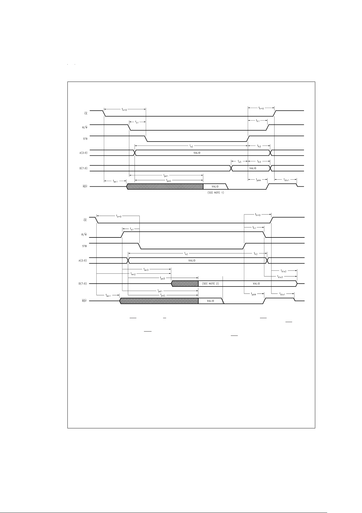
TIMING WAVEFORMS
Note 1: Valid data is provided on the RDY line a t
pd1
after R/W is asserted low or a t
pd2
after valid data is decoded on A2:0. The RDY line will remain high until the
addressed register is ready to participate in the write operation. This condition only applies when writing to a shifter/buffer and is eliminated (i.e., RDY will go low
immediately once valid) when using shifter/buffer status polling (discussed later in this datasheet).
Note 2: Validdata will not appear on D7:0 (and RDY will remain high) until the addressed register is ready to participate in the read operation. When the addressed
register becomes ready (i.e., a byte is available to be read), valid data will be placed on the D7:0 bus and the RDY pin will go low allowing the bus cycle to continue.
This read cycle delay only applies when reading the TDI shifter/buffer and is eliminated when using shifter/buffer status poling.
DS100325-3
FIGURE 2. Write Cycle
DS100325-4
FIGURE 3. Read Cycle
www.national.com 6
Page 7
Parallel Processor Interface (PPI) (Continued)
TIMING WAVEFORMS (Continued)
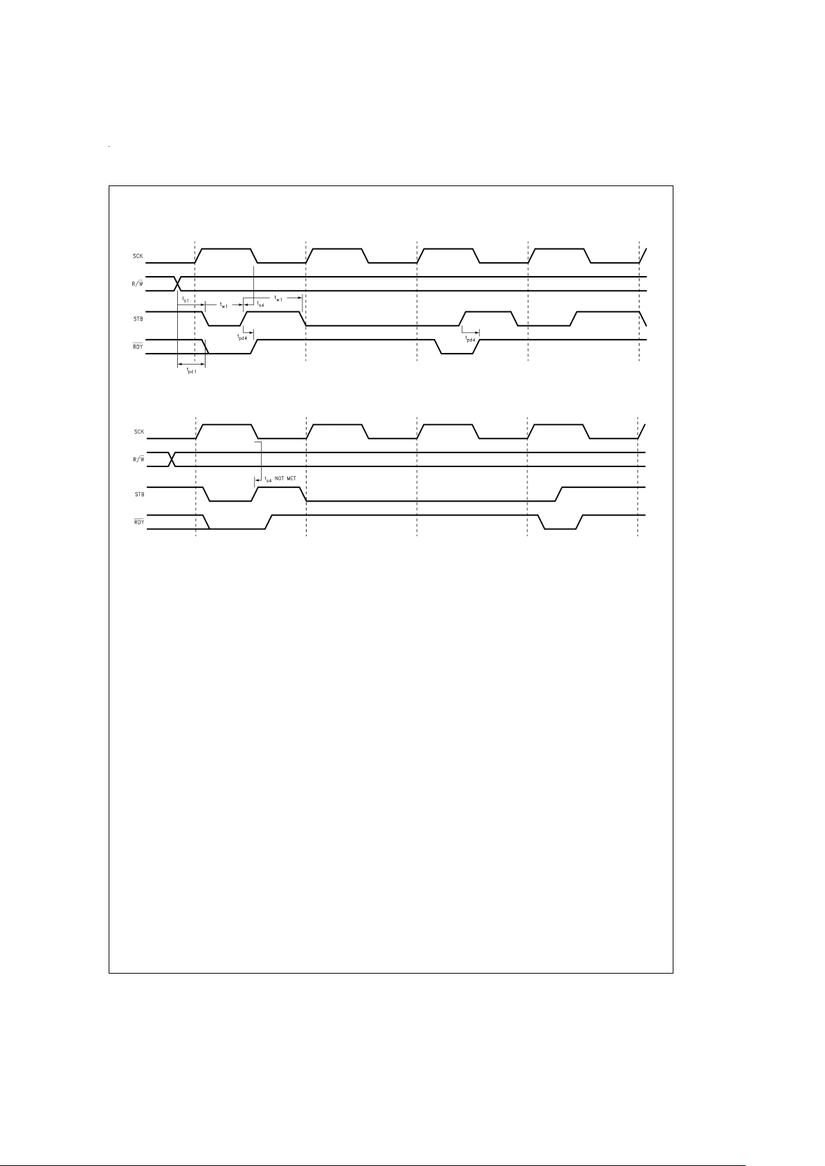
Note 3:
Figures 4, 5:Figure 4
shows the best case bus cycle timing for SCK and STB during consecutive read or write cycles. The rising edge of strobe occurs a
setup time, t
s4
or before the falling edge of SCK. This allows the cycle to be completed within 1.5 clock SCK clock cycles.
Figure 5
shows the worst case bus cycle
timing for SCK and STB during consecutive read or write cycles. The rising edge of strobe does not meet the t
s4
requirement between STB and SCK. Therefore,
the propagation of the internal PSC100 control and reset signals is delayed until the next falling edge of SCK. The bus cycle is then completed 1.5 SCK cycles later
creating a total bus cycle time of 2.5 SCK cycles. If worst case timing is considered for bus cycle timing, t
s4
is not a mandatory timing specification.
DS100325-5
FIGURE 4. Consecutive Read/Writes (best case timing)
DS100325-6
FIGURE 5. Consecutive Read/Writes (worst case timing)
www.national.com7
Page 8
Parallel Processor Interface (PPI) (Continued)
TIMING WAVEFORMS (Continued)
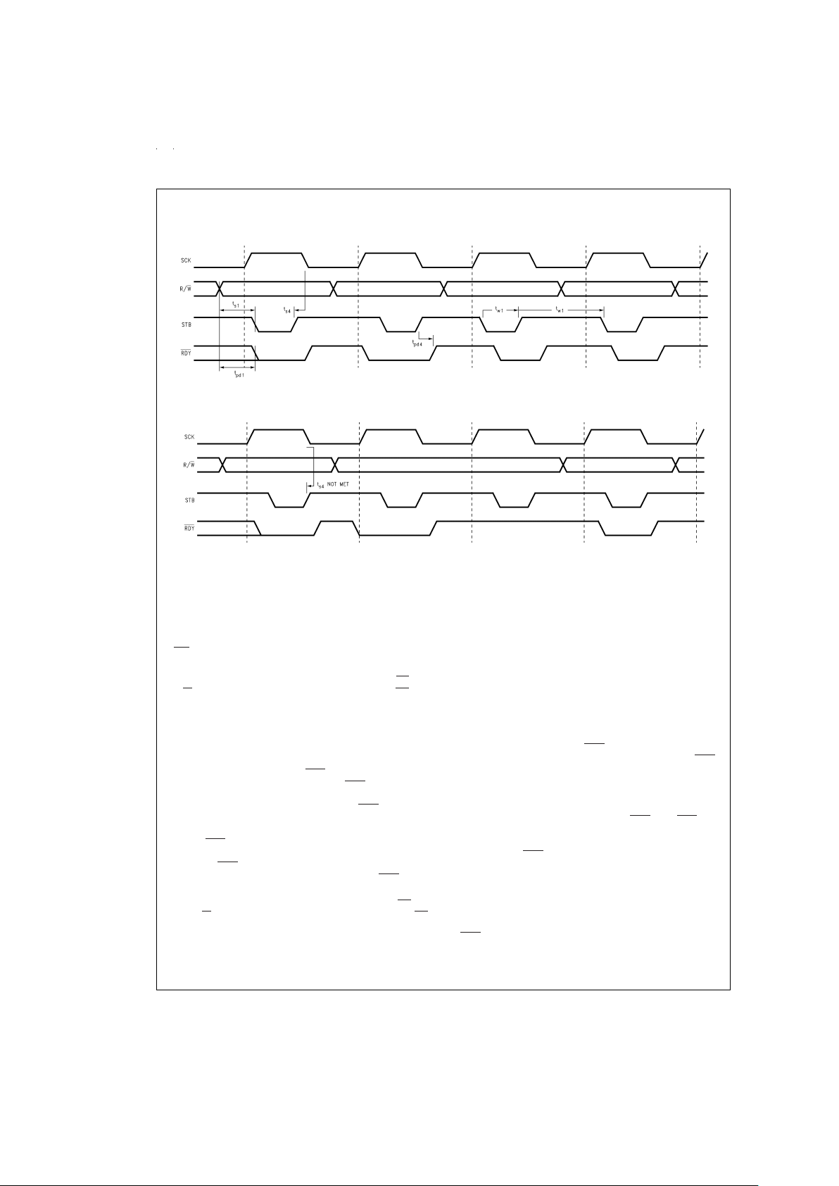
Note 4:
Figures 6, 7
: This diagram shows the timing for a read followed by a write (or write followed by a read). Separate Read and Write data/address latches and
control logic allow consecutive read/write or write/read operations to be overlapped (i.e., do not need to wait 2 or 3 SCK cycles between bus cycles). For the best
case timing scenario (
Figure 6
: rising edge of STB to falling edge of SCK greater than ts4), a new bus cycle can be performed each SCK cycle. For the worst timing
scenario (
Figure 7
: rising edge of STB to falling edge of SCK is less than ts4), a one SCK cycle delay must be included after each back to back read/write or write/
read sequence.
Note 5:
Figures 4, 5, 6, 7
assume that the PSC100 register participating in the bus cycle is ready to accept/provide data. For bus cycles involving a PSC100 shifter/
buffer(s), the ready status of a shifter/buffer can be checked using the status bits in Mode Register 2 prior to the start of the bus cycle. Polling is required when the
RDY pin is not used to provide a processor “handshake”.
READ AND WRITE CYCLES
A Write cycle (see
Figure 2
) is initiated by asserting CE and
R/W low followed by a low on STB a set time later. CE and
STB are gated within the PSC100F and may be asserted
concurrently (i.e., zero setup and hold time). The address is
then asserted on A2:0 to indicate which internal address
within the PSC100F will be written to by the processor. An
address decoder within the PSC100F monitors the address
lines for a valid PSC100F register address. Once a valid address has been decoded, the RDY line becomes active (a
propagation delay time later). The active RDY line will go low
immediately if the addressed register is ready to accept data.
If the addressed register is not ready, the RDY pin will remain high preventing the processor from completing the bus
cycle. Once the register is ready to receive date (see
Table
2
), the RDY pin will go low and processor can resume the
write cycle. The processor then forces a high on STB (a wait
time after RDY goes low) which latches the address (A2:0)
and data (D7:0) completing the bus cycle. The RDY line is
forced high a propagation delay later.
A Read cycle (see
Figure 3
) is initiated by asserting CE low
and R/W high followed by a low on STB a set time later. CE
and STB are gated within the PSC100F and may be asserted concurrently (i.e., zero setup and hold time). The address bits (A2:0) are then asserted to indicate which internal
address within the PSC100F will be read by the processor.
An address decoder within the PSC100F monitors the ad-
dress lines for a valid PSC100F register address. Once a
valid address has been decoded and if the addressed
PSC100F register is ready to be read (see
Table 2
), valid
data is placed on the Data lines (D7:0) a propagation delay
later and the ready line isasserted low.If the addressed register is not ready (e.g., the TDI shifter/buffer is empty), the
ready line will remain high and hold the bus cycle until the
register contains valid data. RDY will then go low allowing
the read cycle to continue. With the high to low edge on RDY
line, the processor can successfully read the valid data.
However,the bus cycle is not completed within the PSC100F
until the rising edge on STB which resets the PSC100F read
logic (required prior to the start of the next read cycle).
Important note concerning the use of RDY : The RDY signal provides a useful “handshake” between the PSC100F
and the processor. However,care must betaken whenusing
the PSC100F RDY signal to prevent a large (or indefinite)
number of processor generated wait states. For example, if
the TDO shifter/buffer is not enabled for shift operations and
the processor writes to the TDO shifter/buffer address 3
times, the two registers which make up the TDO shifter/
buffer will accept the first two bytes of data, but since the
data is not shifting out, the 3rd byte will be held off by the
RDY signal indefinitely. An equally severe problem could result with a finite number of wait states if the application uses
DS100325-20
FIGURE 6. Read/Write or Write/Read (best case timing)
DS100325-7
FIGURE 7. Read/Write or Write/Read (worst case timing)
www.national.com 8
Page 9

Parallel Processor Interface (PPI)
(Continued)
dynamic memories. Holding the local bus with the PSC100F
RDY line long enough to violate a DRAM refresh time will result in lost data within the dynamic memory.
Writing and Reading without the use of RDY : With use of
worst case PSC100F timing, Write and Read cycles can be
successfully completed without the use of the RDY signal.All
read and write cycles will complete within 2.5 SCK cycles
(worst case). Therefore, by assuring at least 2.5 cycles occur
after the rising edge of STB, bus cycles can be completed
without using the RDY “handshake”. The critical timing relationship within the PSC100F for write and read operation is
between the rising edge of STB and the falling edge of SCK.
The rising edge of strobe latches the address/data and also
generates the internal signals required to complete read/
write within the PSC100F (including a signal with resets the
read/write logic and releases the RDY line). The propagation
of these internal signals is initiated on the first falling edge of
SCK after the STB pin is asserted high. If the rising edge on
STB occurs an internal setup time (t
s4
) or greater before the
falling edge of SCK, the bus cycle can be completed within
1.5 SCK cycles (see
Figure 4
). However, if the internal setup
time is not met, the propagation of internal control/reset signals is delayed until the next falling edge of SCK (1 SCK
cycle later) which effectively completes the read/write operation and reset the logic for the next bus cycle within 2.5
cycles (see
Figure 5
). Synchronizing the rising edge of STB
with the falling edge of SCK to assure that t
s4
is met provides
the maximum performance for a read/write operation. However,the asynchronous interface can be used effectively with
software delays, hardware delays or programmed wait
states (to assure 2.5 SCK cycles are completed) toavoid the
need for synchronization.
Consecutive Reads and Writes: Separate control logic and
data/address latches are used for a read and write operation
within the PSC100F.This allows a write to occur after a read
(or conversely, a read to occur after a write) prior to the 1.5/
2.5 SCK clock cycle requirements described above. The timing for a read (or write) followed bya write(or read)is shown
in
Figure 5
and
Figure 6
.
SYNCHRONIZATION
Writes and reads can be synchronized by using any of three
methods: polling, interrupts, or wait state generation:
•
Status bits may be polled to see if a register is ready to be
written to or read from. Tostabilize the status bits for read
operations, the Update Status bit must be set in MODE2
to latch the status.
Note: The status bits only provide the state of the shifter/buffers and do not
indicate that an internal write or read is complete. Therefore, for applications not using the RDY signal to monitor the internal write/read status, timing must be controlled to assure that at least 2.5 SCK cycles
are completed between consecutive read or consecutive write cycles.
•
Any of three different events can be used to generate interrupts by forcing the INT pin high, see
Table 1
.
•
The RDY pin can be used to hold offthe host untilthe addressed register is ready to be accessed. As described
above, this pin can also be used to hold off additional
reads/writes until the synchronizer has recovered from
the previous read/write. RDY=0 signifies that the
’PSC100F is ready to complete the current PPI cycle.
The logic that determines the state of RDY is summarized in
Table 2
.
Reading from CNT32 can be synchronized for testing by using the Single Step Counter mode bit.
TABLE 1. Interrupt Logic
MODE1(7)=1 and TDO MODE1(6)=1 and TDI MODE1(5)=1 and
Shifter/Buffer Not Full Shifter/Buffer Not Empty CNT32 Not Loaded, or at INT
Terminal Count
1XX1
X1X1
XX11
0000
Note 6: Interrupts are generated using the INT pin. Three events trigger INT high. Each event has its own mode bit associated with it for masking or enabling these
interrupts.
www.national.com9
Page 10

Parallel Processor Interface (PPI) (Continued)
TABLE 2. Ready State Logic
R/W
Write
Synchronizer
Busy
TDO TMS0 TMS1 Read
Synchronizer
Busy
TDI
RDY
Shifter/Buffer Shifter/Buffer Shifter/Buffer Shifter/Buffer
Full and Full and Full and Empty and
A(2:0)=0 A(2:0)=2 A(2:0)=3 A(2:0)=1
01XXXXX1
0X1XXXX1
0XX1XXX1
0X X X 1 X X1
00000XX0
1XXXX1X1
1XXXXX11
1XXXX000
Serial Scan Interface (SSI)
TCK CONTROL
TCK CONTROL is the central control block that enables or
disables shift operations and provides byte alignment for the
shifter/buffers. The state of all shifter/buffers and the 32-bit
counter (CNT32) is evaluated here and TCK is stopped and
started.A clock enable circuit allows the “TCK enable” signal
to change only when SCK is low; therefore, TCK always
stops low. TCK does not toggle (remains low) under the following conditions:
•
TDO Shifter/Buffer is enabled and empty.
•
TDO Shifter/Buffer is enabled in PRPG mode and is not
fully loaded.
•
TDI Shifter/Buffer is enabled and full.
DS100325-12
FIGURE 8. 1149.1 (JTAG) TAP Controller State Diagram
www.national.com 10
Page 11

Serial Scan Interface (SSI) (Continued)
•
TDI Shifter/Buffer is enabled in SSC mode but is not fully
loaded with an initial value.
•
TMS0 Shifter/Buffer is enabled and empty.
•
TMS1 Shifter/Buffer is enabled and empty.
•
CNT32 is enabled but not loaded.
•
CNT32 is enabled and has reached terminal count.
Also included within the TCK control block in CNT3, a 3-bit
count up counter. CNT3 is included to maintain byte alignment within the shifter/buffers by providing a signal to toggle
between the two 8-bit FIFOs which comprise the shifter/
buffer. The toggling operation occurs, in an enabled shifter/
buffer,each time CNT3 counts 8 TCK cycles or when CNT32
reaches terminal count. The CNT3 is reset to 0when CNT32
reaches terminal count or after a PSC100 reset condition.
FREEZE MODE. This mode is included in the TCK control
block to support the 1149.1SAMPLE operation. The intent of
the SAMPLE instruction is to allow device input and output
levels to be observed during normal system operation. Data
is latched (or “sampled”) into the boundary scan registers
when the TAP controller (see
Figure 8
on previous page)
transitions from the Capture-DR state to the Shift-DR state (if
SAMPLE/ PRELOAD is the active instruction). Synchronizing this “transition” (rising edge of TCK with TMS at logic low)
with a known system state is imperative to anaccurate pass/
fail assessment. The Freeze Mode provides a means of
asynchronously creating the TCK pulse via an external
PSC100 pin. When the Freeze Pin Enable bit (bit 2 in Mode
Register 1) is set, a logic high on the PSC100 FRZ input pin
will cause TCK to go high. Once the transition is complete,
the Freeze Mode can be removed (i.e. Freeze Pin Enable bit
returned to logic 0 or Freeze pin forced low) and the sampled
data can be shifted out/evaluated using the “standard”
PSC100 protocol.
Figure 9
illustrates the logic implementation of the Freeze feature. It should be noted that Freeze
mode is simply gated with the TCK output and does not disable shift operations within the shifter/buffers or disable
CNT32. Therefore, no shifting or TCK counting using CNT32
should be performed when Freeze mode is enabled.
The “standard” mode of TCK control uses CNT32 in conjunction with the status registers to start and stop TCK. For this
mode, CNT32 is enabled and loaded with the number of
TCK cycles required to shift the desired bits to/from the scan
chain. The shifter/buffer(s) participating in the shift operation
is enabled and provides the necessary full/empty status to
stop TCK for processor writes/reads. This mode of TCK control provides a systematic protocol for managing PSC100
operations (specifically, handling partial bytes). Another option for TCK control relies solely on the status of the shifter/
buffers (i.e., CNT32 is disabled) to start and stop TCK. This
option eliminates the time required to load CNT32, but
makes management of partial bytes (see shifter/buffer description section) more cumbersome.
TMS(1:0) SHIFTER/BUFFERS
The TMS Shifter/Buffer block diagram is shown in
Figure 10
.
These two blocks take parallel data and serialize it for shift
operations through the serial port pins TMS0 and TMS1.
Double-buffering is achieved by configuring the shifter/buffer
asa2x8FIFO. Write and shift operations are controlled by
a local state machine that accepts stimulus from the PPI,
Mode Registers, CNT32 and TCK Control section. The TMS
outputs always change on the falling edge of SCK. The order
of shifting is least significant bit first. TMS(1:0) are forced
high upon RST low. TMS(1:0) are TRI-STATEd when OE is
high.
Write operations are completed if the shifter/buffer is not full
(independent of whether shifter/buffer is enabled or disabled). Otherwise they are ignored. Shifting occurs when the
following conditions are all true:
•
TMS is enabled with its respective mode bit.
•
TMS shifter/buffer is not empty.
DS100325-9
FIGURE 9. TCK Logic
DS100325-10
FIGURE 10. TMS Shifter/Buffer Block Diagram
www.national.com11
Page 12

Serial Scan Interface (SSI) (Continued)
•
TCK is enabled according to the logic in TCK Control.
When shift operations are not enabled, the TMS output retains its last state. During long shift sequences, the TMS
shifter/buffer can be disabled and held static so that shift operations are concentrated only on TDI and TDO. The TMS
output also retains its last state when Test Loop-Back operations are in progress.
Local select circuitry is used to toggle back and forth between the two registers of the “FIFO” when shifting. At any
given time, one register is selected for shift operations. The
other holds its previous state or can accept new parallel
data. Shift register selection changes due to the following
two events:
•
CNT3 in TCK Control signals that 8 bits have been
shifted. This event is used for basic toggling between
each of the two shift registers.
•
CNT32 enabled and at terminal count. This event is used
to account for scan lengths which are not multiples of
eight. When shift register selection changes due to this
signal, any data remaining in the shift register is unused.
AUTO TMS HIGH MODE . This feature is included in the
TMS shifter/buffer block to improve the efficiency of the
PSC100 in supporting shift operations within the 1149.1 devices connected to the SSI. Shifting data and instructions
into 1149.1compliant devices requires that their TAPcontrollers be sequenced to the Shift-DR or Shift-IR states (see
Fig-
ure 8
). Once in this state, shifting occursby holdingTMS low
and clocking TCK. The last bit is shifted when the TAP controller transitions to the EXIT1 state. This transition requires
a logic 1 on TMS. The Auto TMS High feature, enabled by
setting bit 1 of Mode Register 0, automatically creates a logic
1 on the TMS lines of the PSC100 when CNT32=1. Consequently, the last bit is shifted out without having to load specific TMS data into the shifter/buffer.
Note: Auto TMS High mode creates a logic 1 on both TMS lines (i.e., TMS0
and TMS1). Therefore, when using the Auto TMS High feature, all
1149.1 devices connected to the TMS line not participating in the cur-
rent JTAG test operations should be placed in the Test-Logic-Reset
TAP controller state to prevent inadvertent TAP controller transitions.
TDO SHIFTER/BUFFER
The TDO Shifter/Buffer block diagram is shown in
Figure 11
.
This block takes parallel data and serializes it for shift operations through the serial port pin TDO. During normal shift
modes, double-buffering is achieved by configuring the
shifter/buffer asa2x8FIFO. This block can also be configured as a 32-bit Pseudo RandomPattern Generator (PRPG)
with two additional 8-bit parallel-to-serial shift registers. Write
and shift operations are controlled by a local state machine
that accepts stimulus from the PPI,Mode Registers, CNT32,
and the TCK Control section. The TDO output always
changes on the falling edge of SCK. The order of shifting is
least significant bit first. TDO is forced high upon RST low.
TDO is TRI-STATEd when OE is high.
Write operations are completed if the shifter/buffer is not full
(independent of whether shifter/buffer is enabled or disabled). Otherwise they are ignored.
Shifting occurs when the following conditions are all true:
•
TDO is enabled with its respective mode bit.
•
TDO shifter/buffer is not empty.
•
TCK is enabled according to the logic in TCK Control.
When shift operations are not enabled, the TDO output retains its last state. The TDO output also retains its last state
when Test Loop-Back operations are in progress.
Local select circuitry is used to toggle back and forth between the two registers of the “FIFO” when shifting. At any
given time, one register is selected for shift operations. The
other holds its previous state or can accept new parallel
data. Shift register selection changes due to the following
two events:
•
CNT3 in TCK Control signals that 8 bits have been
shifted. This event is used for basic toggling between
each of the two shift registers.
•
CNT32 enabled and at terminal count. This event is used
to account for scan lengths which are not multiples of
eight. When shift register selection changes due to this
signal, any data remaining in the shift register is unused.
PRPG MODE . By setting MODE1(4), the TDO Shifter/Buffer
is reconfigured as a 32-bit PRPG (Pseudo Random Pattern
Generator) using the primitive polynomial:
F(X)=X
32+X22+X2
+X+1
The PSC100 was developed to support both 1149.1 and
non-1149.1 serial test methodologies. Since 1149.1 compliant devices include boundary scan registers on control pins
(i.e. OE), which must remain fixed during boundary scan interconnect testing, generating pseudo-random patterns with
PRPG mode provides limited usefulness for boundary scan
test operations. PRPG mode may provide usefulness in
other serial test or non-test related implementations which
do not require fixed bits in the serial chain.
Figure 12
shows a block diagram of the Linear Feedback
Shift Register hookup.
www.national.com 12
Page 13

Serial Scan Interface (SSI) (Continued)
The PRPG is loaded by four PPI writes to the TDO address.
When the PRPG enable bit is set, apulse isissued internally
that initializes the local parallel load logic such that the
PRPG is loaded sequentially, least significant byte first, most
significant byte last. When in PRPG mode, writes can be
completed at any time; however, shift operations will be disabled until the PRPG is fully loaded.
LOOP AROUND MODE . This mode, enabled by setting bit
0 in Mode Register 0, will cause data appearing at the TDI input to be placed directly back on the TDO output. This fea-
ture can be used for read-only scan operations where data is
shifted into TDI while returning the scan chain to its previous
state when shifting is completed. It can also be used to bypass PSC100 devices connected within a boundary scan
chain (i.e., a PSC100 located within a chain, but not providing the JTAG TAP data). Loop around has limited usefulness
in most boundary scan applications since, typically, data in
the scan chain is shifted out and evaluated as new data is
shifted into the chain for the next test.
DS100325-11
FIGURE 11. TDO Shifter/Buffer Block Diagram Register Hookup
DS100325-14
FIGURE 12. TDO PRPG Block Diagram
www.national.com13
Page 14

Serial Scan Interface (SSI) (Continued)
WRITING A PARTIAL BYTE TO THE TMS0, TMS1 OR
TDO SHIFTER/BUFFER. Since the TMS0, TMS1 and TDO
shifter/buffers shift out least significant bit first, the valid
(meaningful) bits within a partial byte (i.e., byte containing
<
8 valid bits to be shifted to the scan chain) must be stored
and written into the shifter/buffer as the least significant bits.
This will assure that the desired bits will be accurately shifted
to the boundary scan chain. For example, moving the TAP
controllers within the boundary scan chain connected to
TMS0 from the Pause-DR state to the Run-Test/Idlestate requires a 3-bit (110) sequence on TMS0. To provide correct
3-bit sequence on TMS0, the partial byte would be written to
the TMS0 shifter/buffer as:
MSB LSB
xxxxx011→TMS0
A subsequent enable and load of CNT32 with decimal 3 and
enable of theTMS0 shifter/buffer will initialize the shift operation. Terminal count on CNT32 will complete the shift operation. Since terminal count on CNT32 will cause the register
selection to change within the shifter/buffer, the values labeled as “x” will not be used and aretreated as “don’t cares”.
TDI SHIFTER/BUFFER
The TDI Shifter/Buffer block diagram is shown in
Figure 13
.
This block shifts in serial datafrom theTDI portand puts it in
parallel form for read operations at the PPI. During normal
shift modes, double-buffering is achieved by configuring the
shifter/buffer asa2x8FIFO. This block can also be configured as a 16-bit Serial Signature Compactor (SSC). Write,
read, and shift operations are controlled by a local state machine that accepts stimulus from the PPI, Mode Registers,
CNT32 and the TCK Control section. The TDI input always
shifts in data on the rising edge of SCK. The order of shifting
is least significant bit first. The TDI input includes a pull-up
resistor to force a logic 1 when the test data signal returning
from the scan chain is floating.
Read operations are completed if the shifter/buffer is not
empty and SSC mode is not enabled. Otherwise they are ignored. Write operations are only possible while in SSC
mode. Otherwise they are ignored.
Shifting occurs when the following conditions are all true:
•
TDI is enabled with its respective mode bit.
•
TDI shifter/buffer is not full.
•
TCK is enabled according to the logic in TCK Control.
Local select circuitry is used to toggle back and forth between the two registers of the “FIFO” when shifting. At any
given time, one register is selected for shift operations. The
other holds its previous state or can accept new serial data.
Shift register selection changes due to the following two
events:
•
CNT3 in TCK Control signals that 8 bits have been
shifted in. This event is used for basic toggling between
each of the two shift registers.
•
CNT32 enabled and at terminal count. This event is used
to account for scan lengths which are not multiples of
eight. When shift register selection changes due to this
signal, a partial byte (i.e., byte with
<
eight valid data bits
shifted from the scan chain) will exist in the corresponding shift register. The embedded test software functions
written to support the evaluation of data read from the
TDI shifter/buffer must consider bit placement when
reading and evaluating a partial byte.
READING A PARTIAL BYTE FROM THE TDI SHIFTER/
BUFFER. Data is shifted from the scan chain into each TDI
register from most significant bit to least significant bit. Consequently, the valid (i.e., meaningful) bits in a partial byte
shifted into a TDI register will reside in the upper significant
bit locations. For example, if a scan operation involves shifting and evaluating 53 bits returning to TDI, TDI shifter/buffer
must be read 7 times (i.e., 6 full bytes plus apartial byte containing 5 meaningful bits). If the last 5 bits shifted back to the
TDI shifter/buffer are 11010, then upon completion of the
shift operation (i.e., terminal count on CNT32), the shift register within the TDI shifter/buffer will contain the following
partial byte:
MSB LSB
TDI
→
01011xxx
Following a read of a partial byte, the embedded test software must adjust the position of the valid bits read from the
TDI shifter/buffer or the position of the expected data to assure that an accurate comparison is made (and the
non-meaningful bits are masked).
www.national.com 14
Page 15

Serial Scan Interface (SSI) (Continued)
SSC MODE. By setting MODE1(3), the TDI Shifter/Buffer is
reconfigured as a 16-bit SSC (Serial Signature Compactor)
using the primitive polynomial:
F(X)=X
16+X12+X3
+X+1
Within a chain of 1149.1 compliant devices, there are typically one or more input pins which are drivenby uncontrolled
signals (i.e., signals which are not driven to known logic levels during a boundary scan CAPTURE operation). These
signals are masked during the evaluation of data returning
from the scan chain. The SSC within the PSC100 does not
provide masking capabilities and, therefore, provides limited
usefulness for boundary scan test operations. SSC mode
may provide usefulness in other serial test or non-test related implementations which contain predictable data returning into the TDI shifter/buffer.
Figure 14
shows a block diagram of the Linear Feedback
Shift Register hookup.
The SSC is loaded by two PPI writes to the TDI address.
When the SSC enable bit is set, a pulse is issued internally
that initializes the local parallel load logic such that the SSC
DS100325-8
FIGURE 13. TDI Shifter/Buffer Block Diagram
DS100325-13
FIGURE 14. TDI SSC Block Diagram
www.national.com15
Page 16

Serial Scan Interface (SSI) (Continued)
is loaded sequentially,most significant byte first, leastsignificant byte last. When in SSC mode, writes can be completed
at any time; however, shift operations will be disabled until
the SSC is fully loaded. PPI reads from TDI are ignored while
in SSC mode.
Upon leaving SSC mode an internal pulse causes the TDI
shifter/buffer to be full. Also, local read select logic is initialized such that the signature is read most-significant byte
first.
TEST LOOP-BACK MODES. This feature provides a means
for testing ’PSC100 functionality by looping data appearing
at the output of an outgoing shifter/buffer (i.e., TMS0, TMS1
or TDO) back to the input of the TDI shifter/buffer. The loop
back function is accomplished with a simple multiplexer (see
Figure 13
) whose path selection is determined by setting the
mode bits in MODE1(1:0). Loop back does not disable TCK
or prevent shifting of data in the shifter/buffers to the scan
chain(s) connected to the PSC100. Therefore, the state and
operation of the TAP controllers within the scan chain(s)
must be considered when developing Loop-Back test vectors to prevent undesired shifting of data or TAP controller
transitions within the scan chain.
32-BIT COUNTER (CNT32)
CNT32 is a 32-bit, count-down binary counter arranged in
four 8-bit segments. CNT32 can be loaded independent of
its enable/disable status. Loading requires four consecutive
writes to its address (least significant byte first). These four
writes must
not
be interleaved with writes to any other ad-
dress or the CNT32 write control logic will be re-initialized.
This re-initialization will result in a partially filled counter with
an undesired
value
. CNT32 is reset each time the counter
hits terminal count or by asserting the RST pin. A synchronous reset condition (setting Mode2(1)) does not reset the
counter and a new value must be written to CNT32 to provide the desired number of TCK cycles.
SINGLE STEP MODE: All four 8-bit registers are readable
for testability; however,there are no update latches similar to
the ones used for the status bits. To stabilize the counter for
read operations during on-board test, the Single Step Mode
has been added. This allows the user to place CNT32 in any
state and then count for one SCK cycle (TCK will not toggle
when in singled step mode). The result can then be read
from the PPI. The counter can be tested by loading it with
values at its boundary conditions, and then clocking for one
cycle to see the results. For example, the counter could be
loaded with the value:
00000001 00000000 00000000 00000000
The next step is to set the Single Step Mode bit so that the
counter counts down to the next state and stops. The next
value is:
00000000 11111111 11111111 11111111
Four read cycles using the PPI will reveal the results of the
test.
Note: CNT32 will not wrap from terminal count (i.e., 00000000h decremented
by 1 will remain unchanged and will not wrap to FFFFFFFFh). Therefore, CNT32 should be loaded with a non-zero value prior to a Single
Step Mode Operation.
TIMING WAVEFORMS
DS100325-15
FIGURE 15. Serial Scan Interface Timing
www.national.com 16
Page 17

Embedded Test Software Support
A SCANPSC100 device driver is provided by National to
supply functions for performing write, read and shift operations. National also offers a suite of software tools (called
SCAN EASE) which enablesATPG or custom generated test
vectors to be embedded, applied and evaluated within an
IEEE 1149.1 compatible system. SCAN EASE is written to
run on a wide range of processor and memory architectures.
SCAN EASE includes the source code (ANSI C) and is
modular to allow user modification based on application specific needs.
www.national.com17
Page 18

Absolute Maximum Ratings (Note 7)
If Military/Aerospace specified devices are required,
please contact the National Semiconductor Sales Office/
Distributors for availability and specifications.
Supply Voltage (V
CC
) −0.5V to +7.0V
DC Input Diode Current (I
IK
)
V
I
=
−0.5V −20 mA
V
I
=
V
CC
+ 0.5V +20 mA
DC Input Voltage (V
I
) −0.5V to VCC+0.5V
DC Output Diode Current (I
OK
)
V
O
=
−0.5V −20 mA
V
O
=
V
CC
+ 0.5V +20 mA
DC Output Voltage (V
O
) −0.5V to VCC+ 0.5V
DC Output Source/Sink Current (I
O
)
±
50 mA
DC V
CC
or Ground Current
±
50 mA
per Output Pin
DC Latchup Source or Sink Current
±
300 mA
Junction Temperature
Ceramic +175˚C
Storage Temperature −65˚C to +150˚C
ESD Last Passing Voltage (Min) 4000V
Recommended Operating
Conditions
Supply Voltage (VCC)
’PSC100F 4.5V to 5.5V
Input Voltage (V
I
) 0VtoV
CC
Output Voltage (VO) 0VtoV
CC
Operating Temperature (TA)
Military −55˚C to +125˚C
Minimum Input Edge Rate dV/dt
SCAN “F” Series Devices 125 mV/ns
V
IN
from 0.8V to 2.0V
V
CC
@
4.5V, 5.5V
Note 7: Absolute maximum ratings are those values beyond which damage
to the device may occur. The databook specifications should be met, without
exception, to ensure that the system design is reliable over its power supply,
temperature, and output/input loading variables. National does not recommend operation of SCAN outside of recommended operation conditions.
DC Electrical Characteristics
Military
Symbol Parameter V
CC
T
A
=
−55˚C to Units Conditions
(V) +125˚C
Guaranteed Limits
V
IH
Minimum High 4.5 2.0 V V
OUT
=
0.1V or
Input Voltage 5.5 2.0 V
CC
− 0.1V
V
IL
Maximum Low 4.5 0.8 V V
OUT
=
0.1V or
Input Voltage 5.5 0.8 V
CC
− 0.1V
V
OH
Minimum High 4.5 4.4 V I
OUT
=
−50 µA
Output Voltage 5.5 5.4
4.5 3.70 V
IN
=
V
IL
or V
IH
5.5 4.70 V I
OH
=
−24 mA
All Outputs Loaded
V
OL
Maximum Low 4.5 0.1 V I
OUT
=
−50 µA
Output Voltage 5.5 0.1
4.5 0.50 V
IN
=
V
IL
or V
IH
5.5 0.50 V I
OL
=
24 mA
All Outputs Loaded
I
IN
Maximum Input 5.5
±
1.0 µA V
IN
=
V
CC
for TDI, OE
Leakage Current V
IN
=
V
CC
, GND for
All Others
I
ILR
Maximum Input 5.5 −385 µA V
IN
=
GND for
Leakage Current TDI, OE Only
I
OLD
Minimum V
OLD
=
1.65V Max
Dynamic 5.5 50 mA Maximum Test Duration
=
Output Current 2.0 ms, One Output
Loaded at a Time
I
OHD
Minimum V
OHD
=
3.85V Min
Dynamic 5.5 −50 mA Maximum Test Duration=2.0 ms,
Output Current One Output Loaded at a Time
www.national.com 18
Page 19

DC Electrical Characteristics (Continued)
Military
Symbol Parameter V
CC
T
A
=
−55˚C to Units Conditions
(V) +125˚C
Guaranteed Limits
I
OZ
Maximum
±
10.0 µA V
IN
=
V
CC
, GND
TRI-STATE V
IN
(OE , R/W , CE , STB)
=
Leakage Current VIL,V
IH
I
OZT
Maximum I/O
±
11.0 µA V
IN
=
V
CC
, GND
Leakage Current V
O
=
V
CC
, GND
V
IN
(R/W , CE , STB)=VIL,V
IH
I
CC
Maximum
Quiescent
5.5 160 µA TDI, OE Float
Supply Current
I
CCmax
Maximum
Quiescent
5.5 920 µA TDI, OE low
Supply Current
I
CCT
Maximum 5.5 1.60 mA V
IN
=
V
CC
− 2.1V
I
CC
/Input Float: TDI, OE
I
CCTR
Maximum V
IN
=
V
CC
−2.1V
I
CC
/Input 5.5 1.65 mA TDI and OE Only
Float Untested Pin
Note 8: This parameter is not directly testable, but is derived for use in Total Power Supply calculations.
AC Electrical Characteristics/Operating Requirements
Symbol Parameter V
CC
(V)
(Note 9)
Military Units Fig.
No.
T
A
=
−55˚C to +125˚C
C
L
=
50 pF
Min Max
PARALLEL PROCESSOR INTERFACE (PPI)
t
pd1
Prop Delay 5.0 5.5 19.5 ns 2, 3, 4
R/W to RDY
t
pd2
Prop Delay 5.0 5.5 21.0 ns 2, 3
AtoRDY
t
pd3
Prop Delay 5.0 6.5 24.0 ns 3
AtoD
t
pd4
Prop Delay 5.0 7.0 24.0 ns 2–4, 6
STB to RDY
t
pd10
Prop Delay 5.0 7.5 39.0 ns 2–4, 6
SCK to D
t
pd11
Prop Delay 5.0 9.0 34.0 ns 2–4, 6
SCK to INT
t
pd12
Prop Delay 5.0 10.0 36.0 ns 2–4, 6
SCK to RDY
t
en1
Enable Time 5.0 2.0 13.0 ns 2, 3
CE to RDY
t
dis1
Disable Time 5.0 1.5 10.0 ns 2, 3
CE to RDY
t
en2
Enable Time 5.0 1.5 16.5 ns 3
CE to D
www.national.com19
Page 20

AC Electrical Characteristics/Operating Requirements (Continued)
Symbol Parameter V
CC
(V)
(Note 9)
Military Units Fig.
No.
T
A
=
−55˚C to +125˚C
C
L
=
50 pF
Min Max
PARALLEL PROCESSOR INTERFACE (PPI)
t
dis2
Disable Time 5.0 2.5 14.5 ns 3
CE to D
t
en3
Enable Time 5.0 3.0 17.5 ns 3
R/W to D
t
dis3
Disable Time 5.0 3.0 16.0 ns 3
R/W to D
t
en
Enable Time 5.0 3.0 16.0 ns 3
STB to D
t
dis
Disable Time 5.0 2.5 14.5 ns 3
STB to D
t
h1
Hold Time, 5.0 0.5 ns 2–4, 6
R/W to STB
t
s1
Setup Time 5.0 1.0 ns 2–4, 6
R/W to STB
t
h2
Hold Time, 5.0 4.5 ns 2, 3
AtoSTB
↑
t
s2
Setup Time, 5.0 5.0 ns 2, 3
AtoSTB
↑
t
h3
Hold Time, 5.0 4.5 ns 2
DtoSTB
↑
t
s3
Setup Time, 5.0 0.0 ns 2
DtoSTB
↑
t
h
Hold Time, 5.0 1.0 ns 2–4, 6
CE to STB
t
s
Setup Time, 5.0 0.5 ns 2–4, 6
CE to STB
t
s4
Setup Time, 5.0 7.5 ns 4–7
STB
↑
to
SCK
↓
t
h4
Hold Time, 5.0 0.0 ns 4–7
STB
↑
to
SCK
↓
t
h
Hold Time, 5.0 0.0 ns 4–7
STB to RDY
t
W
Clock Pulse
Width, SCK, H
or L
5.0 20.0
ns 4, 6
t
W1
Pulse Width 5.0 6.0 ns 4, 6
STB (H or L)
f
max
Maximum 5.0 25 MHz
Frequency
Clock
www.national.com 20
Page 21

AC Electrical Characteristics/Operating Requirements (Continued)
Symbol Parameter V
CC
(V)
(Note 9)
Military Units Fig.
No.
T
A
=
−55˚C to +125˚C
C
L
=
50 pF
Min Max
SERIAL SCAN INTERFACE (SSI)
t
pd5
Prop Delay 5.0 3.0 14.0 ns 15
SCK to TCK
t
pd6
Prop Delay 5.0 5.5 19.5 ns 15
SCK to TDO
t
pd7
Prop Delay 5.0 4.5 18.5 ns 15
SCK to TMS
t
pd8
Prop Delay 5.0 3.0 13.5 ns 15
FRZ to TCK
t
pd9
Prop Delay 5.0 1.5 10.0 ns 15
TDI to TDO
t
en4
Enable Time 5.0 2.0 13.0 ns 14
OE to JTAG
t
dis4
Disable Time 5.0 1.5 11.0 ns 14
OE to JTAG
t
h5
Setup Time, H
or L, TDI to
SDK (Note
10)
5.0 0.5
ns
15
t
s5
Hold Time, H
or L, TDI to
SDK (Note
10)
5.0 7.5
ns
15
RST RELATED TIMING
t
pd
Prop Delay 5.0 8.0 29.5 ns
RST to D
t
pd
Prop Delay 5.0 8.0 31.0 ns
RST to RDY
t
phl
Prop Delay 5.0 7.0 28.0 ns
RST to INT
t
plh
Prop Delay 5.0 5.5 21.0 ns
RST to TDO
t
plh
Prop Delay 5.0 5.5 20.0 ns
RST to TMS
t
WR
Pulse Width 5.0 6.5 ns
RST (L)
t
REC
Recovery
Time
5.0 1.0 ns
SCK from
RST
Note 9: Voltage Range 5.0 is 5.0V±0.5V.
Note 10: SSC Mode
www.national.com21
Page 22

Application Note
SCK MINIMUM PULSE WIDTH CALCULATION
The SCANPSC100 Parallel to Serial Converter is intended
to act as the interface between a processor and an IEEE
1149.1 boundary scan chain. When used in this configuration, there is a critical timing situation that is not obvious.
This timing involves the system clock rate at whichdata from
the scan ring is being read into the ’PSC100’s TDI pin(target
TAP controllers in SHIFT-DR or SHIFT-IR states).
To fully understand the events which are taking place during
this critical period, it is useful to view the waveforms of interest as they relate in time. See
Figure 16
. The TCK is derived
internally to the ’PSC100 based on the system clock (SCK)
and clock gating control. The result is that when TCK is running, it is at the same frequency as SCK but delayed in time
by the SCK-TCK propagation delay.
The TCK signal from the ’PSC100 drives all of the IEEE
1149.1 target devices. On the rising edge of TCK, data
present at each scan cell is clocked into it. On the falling
edge, this data is presented at the output of the same scan
cell for the next adjacent cell toread. With regards to the last
cell in a particular target, the falling edge of TCK presents
the data in the last scan cell to the TDO pin, a TCK-TDO
propagation delay later.
At the ’PSC100, data shifted in through the TDI pin is
clocked in on the rising edge of SCK, not TCK. The reason
for this is that TCK is generated internal to the ’PSC100 and
intended to control the boundary scan targets. The ’PSC100
is controlled by SCK, therefore the signal to be shifted into
the TDI pin needs to be referenced to SCK not TCK. New
TDI data must be present a TDI-SCK set-up time prior to the
rising edge of SCK in order to guarantee validity. Although
SCK is usually continuous, the TDI buffer is controlled by a
SHIFT-ENABLE signal which is generated internal to the
’PSC100, based on the status of the TDI buffer and the
Mode Registers.
We now see the three major timing components which limit
the duration of the SCK pulse width low. There are two minor
additional delays which should be noted. The TCK signal
from the ’PSC100 needs to arrive at the target device to be
recognized, and this takes a finite amount of time depending
on the signal trace length and impedance. Similarly, the TDO
signal of the last target in the chain needs to reach the TDI
pin of the ’PSC100, taking a finite amount of time as well.
These two trace delays can be minimized by making the target device closest to the ’PSC100 the last device in the
chain. See
Figure 17
.
PROGRAMMING RESTRICTIONS
Because certain mode bits enable shift operations for certain
functions, these mode bits should not be changed when shift
operations are in progress. The alignment of all registers
during shift operations is controlled by a three bit counter in
the TCK control block. Enabling or disabling a function in the
middle of a shift operation may disrupt the logicnecessary to
keep all shifter/buffers byte-aligned. For example, if the TDO
shifter/buffer (already loaded) is enabled while the three bit
counter value is three, the shifter/buffer will only shift out 5
bits of the first byte loaded.
The following bits should not be changed when shift operations are in progress, i.e., when TCK is enabled (see TCK
control section):
•
MODE0(7:3)
•
MODE1(4:3)
•
MODE2(0)
DS100325-16
Pw(L) minimum=Tpd1 + Td1 + Tpd2 + Td2 + Tsu
FIGURE 16. System Clock Timing for Accurate TDI Data
www.national.com 22
Page 23

Application Note (Continued)
DS100325-17
Note:-----Minimize the lengths of these two traces.
FIGURE 17. SCANPSC100 Location Relative to Targets
www.national.com23
Page 24

Physical Dimensions inches (millimeters) unless otherwise noted
28-Pin Leadless Chip Carrier (LCC)
NS Package Number E28A
28-Pin Ceramic DIP
NS Package Number J28A
28-Lead Cerpack
NS Package Number WA28D
www.national.com 24
Page 25

Notes
LIFE SUPPORT POLICY
NATIONAL’S PRODUCTS ARE NOT AUTHORIZED FOR USE AS CRITICAL COMPONENTS IN LIFE SUPPORT
DEVICES OR SYSTEMS WITHOUT THE EXPRESS WRITTEN APPROVAL OF THE PRESIDENT AND GENERAL
COUNSEL OF NATIONAL SEMICONDUCTOR CORPORATION. As used herein:
1. Life support devices or systems are devices or
systems which, (a) are intended for surgical implant
into the body, or (b) support or sustain life, and
whose failure to perform when properly used in
accordance with instructions for use provided in the
labeling, can be reasonably expected to result in a
significant injury to the user.
2. A critical component is any component of a life
support device or system whose failure to perform
can be reasonably expected to cause the failure of
the life support device or system, or to affect its
safety or effectiveness.
National Semiconductor
Corporation
Americas
Tel: 1-800-272-9959
Fax: 1-800-737-7018
Email: support@nsc.com
National Semiconductor
Europe
Fax: +49 (0) 1 80-530 85 86
Email: europe.support@nsc.com
Deutsch Tel: +49 (0) 1 80-530 85 85
English Tel: +49 (0) 1 80-532 78 32
Français Tel: +49 (0) 1 80-532 93 58
Italiano Tel: +49 (0) 1 80-534 16 80
National Semiconductor
Asia Pacific Customer
Response Group
Tel: 65-2544466
Fax: 65-2504466
Email: sea.support@nsc.com
National Semiconductor
Japan Ltd.
Tel: 81-3-5639-7560
Fax: 81-3-5639-7507
www.national.com
SCANPSC100F Embedded Boundary Scan Controller (IEEE 1149.1 Support)
National does not assume any responsibility for use of any circuitry described, no circuit patent licenses are implied and National reserves the right at any time without notice to change said circuitry and specifications.
 Loading...