

Page 1

© 2000 Fairchild Semiconductor Corporation DS010968 www.fairchildsemi.com
December 1991
Revised May 2000
SCANPSC100F Embedded Boundary Scan Controller (IEEE 1149.1 Support)
SCANPSC100F
Embedded Boundary Scan Controller
(IEEE 1149.1 Support)
General Description
The SCANPSC100F is designed to interface a generic parallel processor bus to a se rial scan test bus. It is usef ul in
improving scan throughpu t when applying serial vector s to
system test circuitry and redu ces the software overhead
that is associated with applying serial patterns with a parallel processor. The SCANPSC100F operates by serializing
data from the parallel bus for shi fting through the chain of
1149.1 compliant components (i.e., sc an ch ain ). S ca n da ta
returning from the scan chai n is pla ced on t he para llel po rt
to be read by the host processor. Up to two scan chains
can be directly controlled wi th the SCANPSC1 00F via two
independent TMS pins . Scan control is suppli ed with user
specific patterns which m akes the SCANPSC100F prot ocol-independent. Overflow and underflow conditions are
prevented by stop ping the test clock. A 32 -bit counter is
used to program the number of TCK cycles required to
complete a scan operat ion within the b ounda ry scan chain
or to complete a SCANPSC100F Built-In Self Test (BIST)
operation. SCANPSC100F device drivers and 1149.1
embedded test application code are available with Fairchild’s SCAN Ease software tools.
Features
■ Compatible with IEEE Std. 1149.1 (JTAG) Test Access
Port and Boundary Scan Architecture
■ Supported by Fairchi ld’s SCAN Ease (Embed ded Application Software Enabler) Software
■ Uses generic, asynchronous pr ocessor interface; compatible with a wide range of processors and PCLK frequencies
■ Directly supports up to two 1149.1 scan chains
■ 16-bit Serial Signature Compaction (SSC) at the Test
Data In (TDI) port
■ Automatically produce s pseudo-random patte rns at the
Test Data Out (TDO) port
■ Fabricated on FACT
1.5 µm CMOS process
■ Supports 1149.1 test clock (TCK) frequencies up to
25 MHz
■ TTL-compatible inputs; full-swing CMOS outputs with
24 mA source/sink capability
Ordering Code:
Devices also availab le in Tape and Reel. Specify by appending th e s uffix let t er “X” to the ordering code.
Connection Diagram
FACT is a trademark of Fairchild Semiconductor Corporation.
Order Number Package Numb er Package Description
SCANPSC100FSC M28B 28-Lead Small Outline Integrated Circuit (SOIC), JEDEC MS-013, 0.300 Wide
Page 2

www.fairchildsemi.com 2
SCANPSC100F
Pin Descriptions
Pin Name Description
RST
(Input) The Reset pin is an asynchronous input that, when LOW, initializes the SCANPSC100. Mode bits,
Shifter/Buffer and CNT32 control logic, TCK Control, and the PPI are all initialized to defined states.
RST
has hysteresis for improved noise immunity.
SCK (Input) The System Clock drives all internal timing. The test clock, TCK, is a gated and buffered version of SCK.
SCK has hysteresis for improved immunity.
OE
(Input) Output Enable 3-STATEs all SSI outputs when HIGH. A 20 kΩ pull-up resistor is connected to
automatically 3-STATE these outputs when this signal is floating.
CE
(Input) Chip Enable, when LOW, enables the PPI for byte transfers. D(7:0) and RDY are 3-STATEd if CE is HIGH.
CE
has hysteresis for improved noise immunity.
R/W
(Input) Read/Write defines a PPI cycle—Read when HIGH, Write when LOW.
R/W
has hysteresis for improved noise immunity.
STB (Input) Strobe is used for timing all PPI byte transfers. D(7:0) are 3-STATEd when STB is HIGH. All other PPI
inputs must meet specified setup and hold times with respect to this signal. STB has hysteresis for noise
improved immunity.
A(2:0) (Input) The Address pins are used to select the register to be written to or read from.
D(7:0) (I/O) Bidirectional pins used to transfer parallel data to and from the SCANPSC100.
INT (Output) Interrupt is used to trigger a host interrupt for any of the defined interrupt events. INT is active HIGH.
RDY
(3-STATE Output)
Ready is used to synchronize asynchronous byte transfers between the host and the SCANPSC100.
When LOW, RDY signals that the addressed register is ready to be accessed RDY is enabled when
CE
is LOW
TDO
(3-STATE Output)
Test Data Out is the serial scan output from the SCANPSC100. TDO is enabled when OE
is LOW.
TMS(1:0)
(3-STATE Output)
The Test Mode Select pins are serial outputs used to supply control logic to the UUT.
TMS(1:0) are enabled when OE
is LOW.
TCK
(3-STATE Output)
The Test Clock output is a buffered version of SCK for distribution in the UUT.
TCK Control logic starts and stops TCK to prevent overflow and underflow conditions.
TCK is enabled when OE
is LOW.
TDI (Input) Test Data In is the serial scan input to the SCANPSC100. A 20 k
Ω pull-up resistor is connected to force
TDI to a logic 1 when the TDO line from the UUT is floating.
FRZ (Input) The Freeze pin is used to asynchronously generate a user-specific pulse on TCK. If the FRZ Enable Mode
bit is set, TCK will be forced HIGH if FRZ goes HIGH. FRZ has hysteresis for improved noise immunity.
Page 3

3 www.fairchildsemi.com
SCANPSC100F
Chip Architecture
The SCANPSC100 is designed to act together with a parallel bus host as a serial test bus master. Parallel data is written by the host to the SCANPSC1 00, which serializes the
data for application to a serial test bus. S erial data re turning from the target scan chain(s) is placed on the processor
port for parallel read s. Sev eral fea tures a re i ncluded in the
SCANPSC100 which m ake scan test communic atio n mo re
convenient and efficient.
Figure 1 shows the major functional blocks of the
SCANPSC100 design. The Parallel Processor Interface
(PPI) is an asynchronous, 8-bit parallel interface which is
used by the host processor to write and read data. The PPI
generates the nece ssary internal data, address, and control signals to complete internal write and read operations.
The Serial Scan I nterface ( SSI) consis ts of a b ank of do uble-buffered parallel/seri al shift registers (i.e., a 2 x 8 bit
FIFO), or Shifter/Buffers. The double buffering improves
efficiency by allowing parallel writes or reads to/from one of
the two 8-bit FIFOs wit hin the shifter /buffer while the other
FIFO is shifting data to/fr om th e scan chain. Three Shifte r/
Buffers are provided for outgoing serial data a nd one for
incoming serial data. Test Data Out (TDO) is for scanning
out test data while the two Test Mode Select signals
(TMS0/1) are used to provi de user specific control data.
Test Data In (TDI) receives serial data from the scan chain.
A local control bloc k is associa ted with each Shifte r/Buffer
to provide shift and load control as well a s providing fu ll or
empty status. The SSI also provides T est Clock (TCK) Control. TCK is stopped and started depending on the status of
the Shifter/Buffers or the 32-bit Counter. By stopping and
starting TCK, scan operations w ill proceed only when the
enabled Shifter/Buffers are ready to send and/or receive
serial data.
The 32-bit Counter (CNT32) is a count-down binary
counter included to assist in controlling the SSI. The initial
state of CNT32 is load ed from the parallel port with four
consecutive writes to its address. When enabled, CNT32 is
used to program the number of TCK s app li ed by the SSI to
the boundary scan chain(s). The value o f CNT32 can also
be used to generate i nterrupts (i.e. , when CNT32 reaches
terminal count) and to trigger SCANPSC100 features, such
as, Auto TMS High (discussed later within this datasheet).
The Mode and Status Registe rs are used to control and
observe the opera tion of the SSI and CNT32 . Each of the
Shifter/Buffers and CNT32 have an associated mode bit
which enables it for participation in on-going operations.
Status bits can be used for polling operations.
FIGURE 1. SCANPSC100 Block Diagram
Page 4

www.fairchildsemi.com 4
SCANPSC100F
Mode and Status Registers
MODE REGISTER 0 (MODE0)
This register is purely a mo de register. All bits are writab le
and readable. The value 00100000 is placed in this register
upon RST
low or a synchronous reset operation.
• Bit 7: This bit enables the TDO shifter/buffer for shift
operations. If this bit is set, the TDO shifter/
buffer will cause TCK to stop if it is empty.
• Bit 6: This bit enables t he TDI shifter/bu ffer for shif t
operations. If this bit is set, the TDI shifter/
buffer will cause TCK to stop if it is full.
• Bit 5: This bit enables the 32-bit counter. If this bit is
set, the counter will cause TCK to stop if has
not been loaded or if i t has reached term inal
count.
• Bit 4: This bit enables the TMS0 shifter/buffer for
shift operations. If this bit is set, the TMS0
shifter/buffer will cause TCK to stop if it is
empty.
• Bit 3: This bit enables the TMS1 shifter/buffer for
shift operations. If this bit is set, the TMS1
shifter/buffer will cause TCK to stop if it is
empty.
• Bit 2: This bit is reserved and should rema in as a
logic 0 during all 'PSC100 operations.
• Bit 1: If this bit is set, T MS will be forced high wh en
the 32-bit counter is at state (00000001)h.
• Bit 0: T his bit causes TDI to be connecte d directly
back through TDO for Loop-Around operations.
MODE REGISTER 1 (MODE1)
This register is purely a mo de register. All bits are writab le
and readable. The value 00000000 is placed in this register
upon RST
low or a synchronous reset operation.
• Bi t 7: If this bit is set and the TDO shifter/ buffer is
not full (i.e., one or both 8-bit TDO FIFOs are
empty), the INT pin will go HIGH.
• Bit 6: If this bit is set and the TDI shifter/buffer is not
empty (i.e., one or both 8-bit TDI FIF Os are
full), the INT pin will go HIGH.
• Bit 5: If this bit is set, and the 32-bit counter is not
loaded or has reached terminal count, the INT
pin will go HIGH.
• Bit 4: This bit signifies that the TD0 shifter /buffer is
reconfigured as a 32-Bit Pseudo Random Pattern Generator. If set, and MODE0 Bit 7 is set,
the TDO shifter/buffer will stop TCK until a
seed value has been written to al l four of the
8-bit LFSR segments.
• Bit 3: This bit signifies that the TD1 shifter /buffer is
reconfigured as a 16-Bit Serial Signature
Compactor. If set, and MODE0 Bit 6 is set, the
TDI shifter/buffer will cause TCK to stop until
a seed value has been written to the tw o TDI
registers.
• Bit 2: If this bit is set, a high value on FRZ will force
TCK high (see TCK Control Section).
• Bits 1 and 0: These bits are used to control Test LoopBack operations according to the following
table.
Bit 7 Bit 6 Bit 5 Bit 4 Bit 3 Bit 2 Bit 1 Bit 0
TDO TDI CNT32 TMS0 TMS1 Auto TMS High Loop-Around
Enable Enable Enable Enable Enable Reserved Enable Enable
Bit 7 Bit 6 Bit 5 Bit 4 Bit 3 Bit 2 Bit 1 Bit 0
TDO TDI CNT32 PRPG SSC Freeze Test Test
Interrupt Interrupt Interrupt Enable Enable Pin Loop- Loop-
Enable Enable Enable Enable Back Back
MODE1 MODE1 Function
Bit 1 Bit 0
0 0 Normal Operation
0 1 Loop-Back TDO to TDI
1 0 Loop-Back TMS0 to TDI
1 1 Loop Back TMS1 to TDI
Page 5

5 www.fairchildsemi.com
SCANPSC100F
Mode and Status Registers (Continued)
MODE REGISTER 2 (MODE2)
Write:
Read:
This register cont ains both mod e and status bits. Bits 4 –7
are status bits only. Bit 3 is a status bit d uring rea d operations and a mode bit during writ e operations. Bits 0–2 are
mode bits only. Upon RST
low, or a synchronous reset, the
value placed in MO DE2 is 10111000 (Rea d mode ). Lat che s
used to update status bits 3–7 retain their last state upon
RST
and are in an “unknown” state after power-up. To initialize the latches to a known state, they need to be
updated using the Update Status bit (bit 2) or continuous
update bit (bit 3).
• Bit 7: Set high if the TDO shifter/ buffer is not full,
i.e., one or both 8-bit TDO FI FOs are ready to
be written to.
• Bit 6: Set hig h if the TDI shifter/buffer is not empty,
i.e., one or both 8-bit T DI FIFOs are re ady to
be read from.
• Bit 5: Set high if the 32-bit counter has not been
loaded, or has reached terminal count.
• Bi t 4: Set h igh if the TMS0 shifter/buffer is not full,
i.e., one or both 8-bi t TMS0 FIFOs are rea dy
to be written to.
• Bit 3 (Read Cycle):
Set high if the TMS1 shi fter/buffer is not full,
i.e., one or both 8-bi t TMS1 FIFOs are rea dy
to be written to.
• Bit 3 (Write Cycle):
If set, will cause all status bits to be continuously updated.
• Bit 2 (Read Cycle):
Shows the state of the Continuous Update bit
during read operations (Bit 3 during writes).
• Bit 2 (Write Cycle):
If set, will cause a pulse to be issued internally
that will update all status bits. This bit will be
reset upon completion of th e pulse. T he state
of this bit is not readable. It is rese t upo n R ST
low.
• Bit 1: If set, will cause a synchronous reset of all
functions except the parallel interface. The
value of this bit will return to zero when t he
reset operation is complete.
• Bit 0: If set, will cause the 32-bit counter to count for
one SCK cycle (no TCK cycle will be generated). The value of this bit will return to zero
when the single step operation is complete.
PROGRAMMING RESTRICTIONS
Because certain mo de bit s enable shift o perations for certain functions, these mode bits should not be changed
when shift operati ons are in prog ress . The a lignm ent o f al l
registers during shift operations is controlled by a 3-bit
counter in the TCK control block . Enabling or disabling a
function in the middle of a shi ft operation may dis rupt the
logic necessary to keep all shifter/buffers byte-aligned.
For example, if the TDO shi fter/buffer (already loaded) i s
enabled while the 3 -b it cou nte r value is 3, the shifter /bu ffer
will only shift out only five bits of the first byte loaded.
The following bits should not be changed when shift operations are in progress, i.e. , when TCK is enab led (see section on TCK Control).
• MODE0(7:3)
• MODE1(4:3)
• MODE2(0)
Parallel Processor Interface (PPI)
ADDRESS ASSIGNMENT
The following table defines which r egister is selected for
access with the address lines, A(2:0).
Bit 7 Bit 6 Bit 5 Bit 4 Bit 3 Bi t 2 Bit 1 Bit 0
Not Not Not Not Continuous Update Single
Used Used Used Used Update Status Reset Step
CNT32
Bit 7 Bit 6 Bit 5 Bit 4 Bit 3 Bit 2 Bit 1 Bit 0
TDO TDI CNT32 TMS0 TMS1 Continuous Single
Status Status Status Status Status Update Reset Step
CNT32
A2 A1 A0 R/W Function
0 0 0 0 TDO Shifter/Buffer
0 0 0 1 Counter Register 1
0 0 1 0 TDI Shifter/Buffer
0 0 1 1 TDI Shifter/Buffer
0 1 0 0 TMS0 Shifter/Buffer
0 1 0 1 Counter Register 2
0 1 1 0 TMS1 Shifter/Buffer
0 1 1 1 Counter Register 3
1 0 0 0 32-Bit Counter
1 0 0 1 Counter Register 0
1010MODE0
1011MODE0
1100MODE1
1101MODE1
1110MODE2
1111MODE2
Page 6

www.fairchildsemi.com 6
SCANPSC100F
Parallel Processor Interface (PPI) (Continued)
TIMING WAVEFORMS
FIGURE 2. Write Cycle
FIGURE 3. Read Cycle
Note 1: Valid data is provided on the RDY line a t
PD1
after R/W is asserted LOW or a t
PD2
after valid data is decoded on A2:0. The RDY line will remain HIGH
until the addresse d register is rea dy to participa te in the write o peration. Th is condition only applies w hen writing to a shifter/buffer an d is eliminated (i.e.,
RDY
will go LOW immedia te ly once valid) when using shif t er/buffer status polling (dis c us s ed later in this datasheet ).
Note 2: Valid data will not appear on D7:0 (and RDY
will remain HIGH) until the addressed register is ready to participate in the read operation. When the
addressed regist er bec om es rea dy (i.e. , a byt e is avai lab le to be read), valid data will be p lace d on th e D7:0 b us and the R DY
pin will go LOW allowing t he
bus cycle to continue. This read cycle delay only applies when reading the TDI shifter/buffer and is eliminated when using shifter/buffer status poling.
Page 7

7 www.fairchildsemi.com
SCANPSC100F
Parallel Processor Interface (PPI) (Continued)
TIMING WAVEFORMS (Continued)
FIGURE 4. Consecutive Read/Writes (best case timing)
FIGURE 5. Consecutive Read/Writes (worst case timing)
Note 3: Figures 4, 5: Figure 4 shows the best case bus cycle timing for SCK and STB during consecutive read or write cycles. The rising edge of strobe
occurs a setup time, t
S4
or before the falling edge of SCK. This allows the cycle to be completed within 1.5 clock SCK clock cycles. Figure 5 shows the worst
case bus cycle timing for SCK and STB during consecutive read or write cycles. The rising edge of strobe does not meet the t
S4
requirement betw een ST B
and SCK. Theref ore, the propa gation of the in ternal P SC100 cont rol and r eset signals is delay ed unt il the n ext fall ing edge of SCK. The bus cycle is then
completed 1.5 SCK cycles later creating a total bus cycle time of 2.5 SCK cycles. If worst case timing is considered for bus cycle timing, t
S4
is not a manda-
tory timing specifica tio n.
FIGURE 6. Re ad/Write or Write/Read (best case timing)
FIGURE 7. Read/Write or Write/Read (worst case timing)
Note 4: Figures 6, 7: This diagram shows the timing for a read followed by a write (or write followed by a read). Separate Read and Write data/address
latches and control log ic allow cons ecutive re ad/write or write/read o perations to be overlapp ed (i.e., do n ot need to wait 2 or 3 SCK cycles between bus
cycles). For the best case timing scenario (Figure 6: rising edge of STB to falling edge of SCK greater than tS4), a new bu s c ycle can be performed each SCK
cycle. For the worst timing scenario (Figure 7: rising edge of STB to falling edge of SCK is less than t
S4
), a one SCK cycle delay must be included after each
back to back read/writ e or write/read sequence.
Note 5: Figures 4, 5, 6, 7 assume that the PSC100 register participating in the bus cycle is ready to accept/provide data. For bus cycles involving a PSC100
shifter/buffer(s), the re ady status of a shifter/buffer c an be checke d using the stat us bits in Mod e Register 2 pr ior to the start of the bus cycle. Polling is
required when the RDY
pin is not used to provide a processor “handshake”.
Page 8

www.fairchildsemi.com 8
SCANPSC100F
Parallel Processor Interface (PPI) (Continued)
READ AND WRITE CYCLES
A Write cycle (see Figure 2) is initiated by asserting CE
and R/W low followed by a LOW on STB a set time later.
CE
and STB are gated wi thin the PSC100F and may b e
asserted concurrentl y (i.e., zer o setup a nd hold time). Th e
address is then asserted on A2:0 to indicate which internal
address within the PSC100F will be written to by the processor. An address decoder within th e PSC100F monito rs
the address lines f or a valid PSC100F register ad dress.
Once a valid address has been decoded, the RDY
line
becomes active (a propagation delay time later). The active
RDY
line will go LOW immediately if the addressed register
is ready to accept data. If the addressed register is not
ready, the RDY
pin will remain HIGH preventing the processor from completing the bus cycle. Once the reg ister is
ready to receive date (s ee Table 2), the RDY
pin will go
LOW and processor can resume the write cycle. The processor then forces a HIGH on STB (a wait time a fter RDY
goes LOW) which latches the address (A2:0) and data
(D7:0) completing the bus cycle. The RDY
line is forced
HIGH a propagation delay later.
A Read cycle (see Figure 3) is initiated by asserting CE
LOW and R/W HIGH followed by a LOW on STB a set time
later. CE
and STB are gated withi n the PSC100F and m ay
be asserted concurre ntly (i.e., zero setup and hold time).
The address bits (A2:0) are then asserted to indicate which
internal address with in the PSC100F will be read by the
processor. An address decoder within the PSC100F monitors the address lines for a valid PSC100F register
address. Once a valid address has been decoded and if
the addressed PSC100 F register is ready to b e read (see
Table 2), valid data is placed on the Data lines (D7:0) a
propagation delay later and the ready line is asserted LOW.
If the addressed register is not ready (e.g. , the TDI shifte r/
buffer is empty), the ready line will remain HIGH and hold
the bus cycle until the register contains valid data. RDY
will
then go LOW allowing the read cycle to con tinue. Wit h the
HIGH-to-LOW edge on RDY
line, the processor can successfully read the valid data . Ho weve r, the bus cycle is n ot
completed within the PSC100F until the rising edge on STB
which resets the PSC10 0F rea d logi c (requ ired prio r to the
start of the next read cycle).
Important note concerning the use of RDY
: The RDY
signal provides a useful “handshake” between the
PSC100F and the processor. However, care must be taken
when using the PSC100F RDY
signal to prevent a large (or
indefinite) numbe r of processor genera ted wait states. Fo r
example, if the TDO shifter/buffer is not enabled for shift
operations and the processor writes to the TDO shifter/
buffer address 3 times, the two registers which make up
the TDO shifter/buffer will accept the first two bytes of data,
but since the data is not shiftin g out, the 3rd byte will be
held off by the RDY
signal indefinitely. An equally sever e
problem could resu lt with a finite number of wait states if
the application use s dynamic memo ries. Holding t he local
bus with the PSC100F RDY
line long enough to violat e a
DRAM refresh time will result in lost data within the
dynamic memo ry.
Writing and Reading without the use of RDY
: With use
of worst case PSC100F timin g, Write a nd Rea d cyc les ca n
be successfully comple ted witho ut the use of t he RDY
signal. All read and write cycles will complete within 2.5 SCK
cycles (worst case). Therefore, by assuring at least 2.5
cycles occur after the rising edge of STB, b us cycles can
be completed without using the RDY
“handshake”. The critical timing relationship within the PSC100F for write and
read operation is betwee n the rising edge of STB an d the
falling edge of SCK. The rising edge of strobe latches the
address/data and also generates the internal signals
required to complete read/write within the PSC100F
(including a signal with resets the read/write logic and
releases the RDY line ). The propagation o f these internal
signals is initiated on the first falling edge of SCK after the
STB pin is asserted HIGH. If the rising edge on STB occurs
an internal setup time (t
S4
) or greater before the falling
edge of SCK, the bus cycle can be comp leted within 1.5
SCK cycles (see Figure 4). However, if the internal setup
time is not met, the propagat ion of internal control/reset
signals is delayed until the next falling edge of SCK (1 SCK
cycle later) which effectively completes the read/write operation and reset the logic for the next bus cycle within 2.5
cycles (see Figure 5). Synchronizing the rising edge of STB
with the falling edge of SCK to assur e that t
S4
is met pro-
vides the maximum performance for a read/write operation.
However, the asynchronous interface can be used effectively with software delays, hardware delays or programmed wait states (to assure 2.5 SCK cycles are
completed) to avoid the need for synchronization.
Consecutive Reads and Writes: Separate control logic
and data/address latche s are used for a read and write
operation within the PSC100F. This allows a write to occur
after a read (o r conversely, a read to occur after a write)
prior to the 1.5/2.5 SCK clock cycle requirements
described above. The timing for a read (or write) followed
by a write (or read) is shown in Figure 5 and Figure 6.
SYNCHRONIZATION
Writes and reads can be synchronized by using any of
three methods: polling, interrupts, or wait state generation:
• Status bits may be polle d to see if a register is ready to
be written to or read from . To stabilize the status bits for
read operations, the Update Status bit must be set in
MODE2 to latch the status.
Note: The status bits only provide the state of the shifter/buffers and do not
indicate that an internal write or read is complete. Therefore, for applications not usi ng the RDY
signal to monitor the internal write/read status, timing must be c ontrolled to as s ure that at l east 2.5 SCK cycles are completed
between consecut iv e read or consecutive wr ite cyc les.
• Any of three different events can be us ed to generate
interrupts by forcing the INT pin HIGH, see Table 1.
• The RDY
pin can be used to hold off the ho st until the
addressed register is ready to be accessed. As
described above, this pi n can also be used to hold off
additional reads/writes until the synchr onizer ha s recovered from the previous read/write. RDY
= 0 signifies that
the SCANPSC100F is ready to complete the current PPI
cycle. The logic that determines the state of RDY
is
summarized in Table 2.
Reading from CNT32 can be synchronized f or testing by
using the Single Step Counter mode bit.
Page 9
9 www.fairchildsemi.com
SCANPSC100F
Parallel Processor Interface (PPI) (Continued)
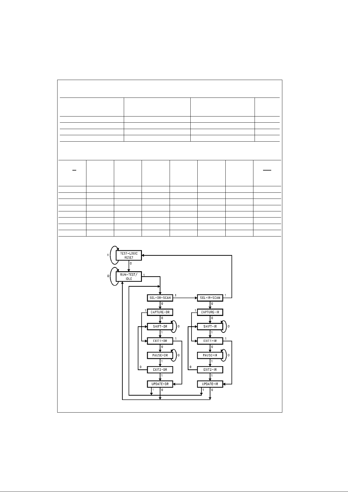
TAB LE 1. Interrupt Logic
Note 6: Interrupts are generated using the INT pin. Three events trigger INT HIGH. Each event has its own mode bit associated with it for masking or
enabling these interrupts.
TABLE 2. Ready State Logic
FIGURE 8. 1149.1 (JTAG) TAP Controller State Diagram
MODE1(7)
= 1 and TDO MODE1(6) = 1 and TDI MODE1(5) = 1 and
Shifter/Buffer Not Full Shifter/Buffer Not Empty CNT32 Not Loaded, or at INT
Terminal Count
1XX1
X1X1
XX11
0000
R/W
Write
Synchronizer
Busy
TDO TMS0 TMS1 Read
Synchronizer
Busy
TDI
RDY
Shifter/Buffer Shifter/Buffer Shifter/Buffer Shifter/Buffer
Full and Full and Full and Empty and
A(2:0)
= 0A(2:0) = 2 A(2:0) = 3A(2:0) = 1
01XXXXX1
0X1XXXX1
0XX1XXX1
0XXX1XX1
00000XX0
1XXXX1X1
1XXXXX11
1XXXX000
Page 10
www.fairchildsemi.com 10
SCANPSC100F
Serial Scan Interface (SSI)
TCK CONTROL
TCK CONTROL is the central control block that enables or
disables shift operatio ns and provides byte alignmen t for
the shifter/buffers. The state of all shifter/buffers and the
32-bit counter (CNT32) is evaluated here and TCK is
stopped and started. A clock enable circuit allows the “TCK
enable” signal to change only when SCK is LOW; therefore, TCK always stops LOW. TCK does not toggle
(remains LOW) under the following conditions:
• TDO Shifter/Buffer is enabled and empty.
• TDO Shifter/Buffer is enab led in P RPG m ode an d is n ot
fully loaded.
• TDI Shifter/Buffer is enabled and full.
• TDI Shifter/Buffer is enabled in SSC mode but is not fully
loaded with an initial value.
• TMS0 Shifter/Buffer is enabled and em pty.
• TMS1 Shifter/Buffer is enabled and em pty.
• CNT32 is enabled but not loaded.
• CNT32 is enabled and has reached terminal count.
Also included within the TCK co ntr ol blo ck i n CNT 3, a 3- bit
count up counter. CNT3 is included t o mainta in byte alignment within the shifter/buffer s by pr oviding a si gnal to toggle between the two 8-bit FIFOs which comprise the shifter/
buffer. The toggling operation occurs, in an enabled shifter/
buffer, each time CNT3 counts 8 TCK cycles or when
CNT32 reaches terminal count. The CNT3 is reset to 0
when CNT32 reaches terminal count or after a PSC100
reset condition.
FREEZE MODE. This mode is included in the TCK c ontrol
block to support the 1149.1 SAMPLE operati on. The intent
of the SAMPLE instruction is to allow device input and output levels to be observed during no rmal system oper ation.
Data is latched (or “sampled”) into the boundary scan reg-
isters when the TAP controller (see Figur e 8 on previous
page) transitions from the Capture-DR state to the Shift-DR
state (if SAMPLE/ PRELOAD is the active instruction).
Synchronizing this “transition” (rising edge of TCK with
TMS at logic low) with a known system state is imp erative
to an accurate pass/fail assessment. The Freeze Mode
provides a means of asynchronously creating the TCK
pulse via an external PSC10 0 pin. When the Freeze Pin
Enable bit (bit 2 in Mode Reg ister 1) is s et, a lo gic h igh on
the PSC100 FRZ input pin will cause TCK to go HIGH.
Once the transition is complete, the Freeze Mode can be
removed (i.e. Freeze Pin Enable bit returned to logic 0 or
Freeze pin forced LOW) and the sampled data can be
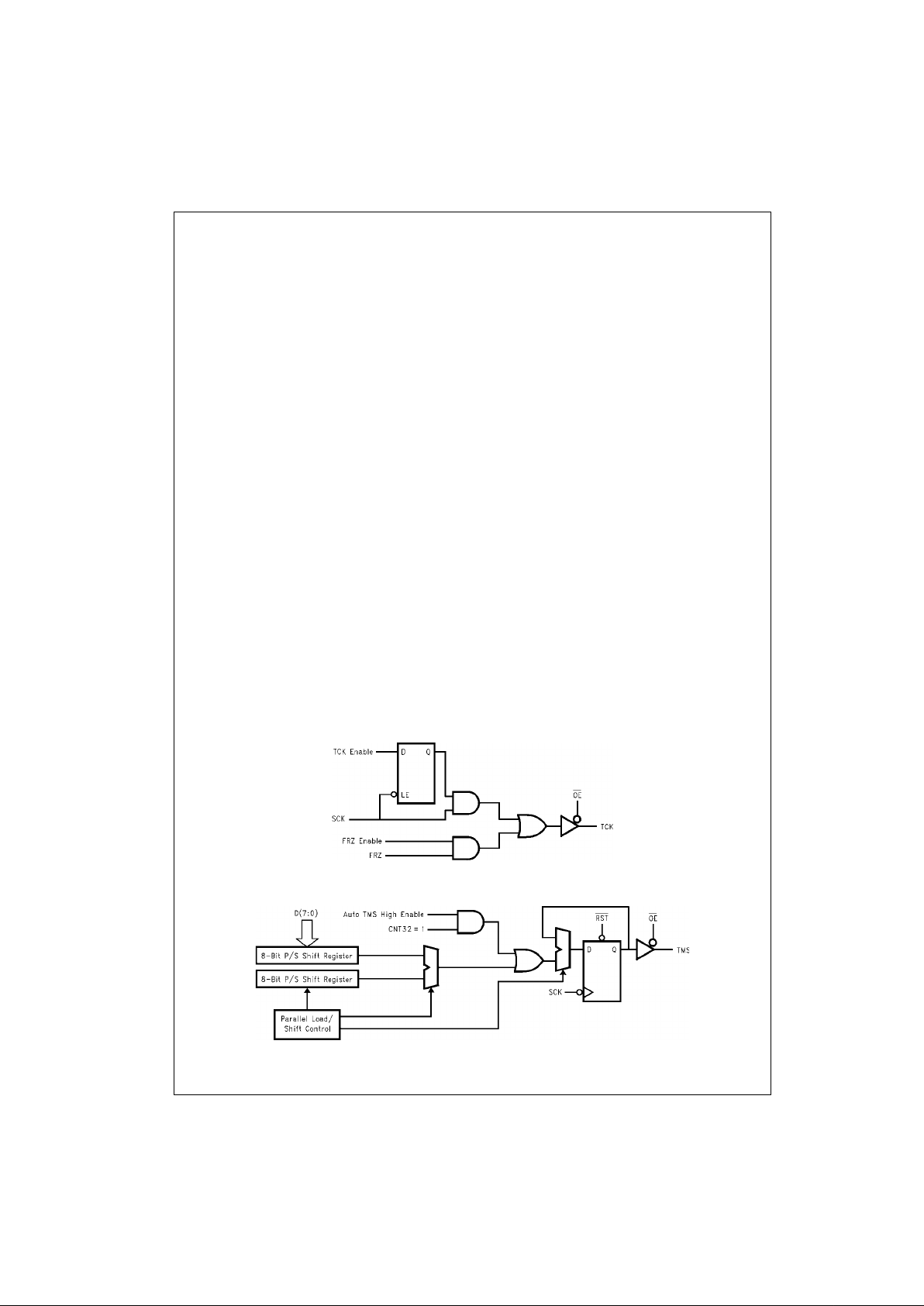
shifted out/evaluated using the “standard” PSC100 pro tocol. Figure 9 illustrates the logic implementation of the
Freeze feature. It should be noted that Freeze mode is simply gated with the TCK ou tput and does not disable shift
operations within the shifter/buffers or disable CNT32.
Therefore, no shifting or TCK counting using CNT32
should be performed when Freeze mode is enabled.
The “standard” mode of TCK control uses CNT 32 in conjunction with the status registers to start and stop TCK. For
this mode, CNT3 2 is enab led a nd loaded with the numb er
of TCK cycles required to shift the desired bits to/from the
scan chain. The s hifter/buffer(s) participating in the shift
operation is enabled and provides the necessary full/empty
status to stop TCK for pr ocessor writes/reads. This mode
of TCK control provides a systematic protocol for managing
PSC100 operations (specifically, handling partial bytes).
Another option for TCK control relies solely on the status of
the shifter/buffers (i.e., CNT32 is disabled) to start and stop
TCK. This option eliminates the time required to load
CNT32, but makes management of partial bytes (see
shifter/buffer description s ectio n) mor e cumb ersome.
FIGURE 9. TCK Logic
FIGURE 10. TMS Shifter/Buffer Block Diagram
Page 11

11 www.fairchildsemi.com
SCANPSC100F
Serial Scan Interface (SSI) (Continued)
TMS(1:0) SHIFTER/BUFFERS
The TMS Shifter/Bu ffer block diagram is shown in Figure
10. These two blocks take paralle l data and serialize it for
shift operations through the serial port pins TMS0 and
TMS1.
Double-buffering is achieved by configuring the shifter/
buffer as a 2 x 8 FIF O. Write a nd sh ift opera tions a re co ntrolled by a local state ma chine that acce pts stimulus fro m
the PPI, Mode Registers, CNT32 and TCK Control section.
The TMS outputs always change on the falling edge of
SCK. The order of shifting is least significant bit first.
TMS(1:0) are forced HIGH up on RST
LOW. TMS(1:0) are
3-STATEd when OE
is HIGH.
Write operations are co mpleted if the shifter/buffer is not
full (independent of whether shifter/buffer is enabled or disabled). Otherwise they are ignored . Shifting occurs w hen
the following conditions are all true:
• TMS is enabled with its respective mode bit.
• TMS shifter/buffer is not empty.
• TCK is enabled according to the logic in TCK Control.
When shift operations are not enabled, the TMS output
retains its last state. During long shift seque nces, the TMS
shifter/buffer can be disa bled and held static so that shift
operations are concentrated only on TDI and TDO. The
TMS output also retains its last state when Test Loop-Back
operations are in progress.
Local select circuitry is used to toggle back and forth
between the two registe rs of the “FIFO” when shift ing. At
any given time, one register is selected for shift operations.
The other holds its previous state or can accept new parallel data. Shift register selection ch anges due to the fo llowing two events:
• CNT3 in TCK Control signals that 8 bits have been
shifted. This event is used for basic toggling between
each of the two shift registers.
• CNT32 enabled and at terminal count. This event is
used to account for scan lengths which are not multiples
of eight. When shift register selection changes due to
this signal, any data remaining in the shift register is
unused.
AUTO TMS HIGH MODE. This feature is inclu ded in the
TMS shifter/buffer block t o improve the efficiency of the
PSC100 in supporting shift operations within the 1149.1
devices connected to the SSI. S hifting data and instructions into 1149.1 compliant d evices r equire s that thei r TAP
controllers be sequen ced to the Shift- DR or Shif t-IR sta tes
(see Figure 8). Once in this state, shifting occurs by holding
TMS LOW and cloc king TCK. The last bit is shi fted when
the TAP controller transitions to the EXIT1 state. This transition requires a logic 1 on TMS. The A uto TMS High fe ature, enabled by setting bit 1 of Mode Register 0,
automatically create s a logic 1 on the TMS lines of the
PSC100 when CNT32
= 1. Consequently, the last bit is
shifted out without hav ing to load specific TMS data into
the shifter/buffer.
Note: Auto TMS High mode creates a logic 1 on both TMS lines (i.e., TMS0
and TMS1). Therefore, when using the Auto TMS High feature, all 1149.1
devices connected to the TMS line not participating in the current JTAG test
operations should be placed in the Test-Logic-Reset TAP controller st at e t o
prevent inadverten t TAP controller transitions.
TDO SHIFTER/BUFFER
The TDO Shifter/Buffer block di agram is shown in Figure
11. This block takes parallel data an d serializes it for shi ft
operations through the serial po rt pin TDO. Du ring normal
shift modes, double-buffering is achieved by configuring
the shifter/buffer as a 2 x 8 FIFO. This block can also be
configured as a 32-bit Pse udo Random Pat tern Generator
(PRPG) with two additional 8-bit parallel-to-serial shift registers. Write and shift o perations are contro lled by a local
state machine that accepts stim ulus from the PPI, Mode
Registers, CNT32, and the TCK C ontrol secti on. The TDO
output always changes on the falling edge of SCK. The
order of shifting is le ast significant bit first. TDO is forced
high upon RST
LOW. TDO is 3-STATEd when OE is HIGH.
Write operations are c ompleted if the shifter/buffer is not
full (independent of whether shifter/buffer is enabled or disabled). Otherwise they are ignored.
Shifting occurs when the following conditions are all true:
• TDO is enabled with its respective mode bit.
• TDO shifter/buffer is not empty.
• TCK is enabled according to the logic in TCK Control.
When shift operations are not enabled, the TDO output
retains its last state. The TDO o utput also retains its last
state when Test Loop-Back operations are in progress.
Local select circuitry is used to toggle back and forth
between the two regis ters of the “FIFO” when shifting. At
any given time, one register is selected for shift operations.
The other holds its previo us sta te or can ac cept new pa rallel data. Shift registe r selection changes du e to the f ollowing two events:
• CNT3 in TCK Control signals that 8 bits have been
shifted. This event is used for basic to ggling between
each of the two shift registers.
• CNT32 enabled and at terminal count. This event is
used to account for scan lengths which are not multiples
of eight. When shift register selection changes due to
this signal, any data remaining in the shift register is
unused.
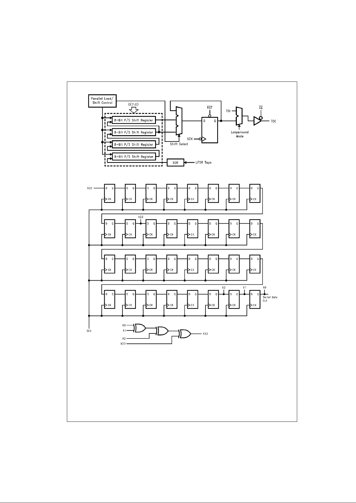
PRPG MODE. By setting MODE1(4), the TDO Shifter/
Buffer is reconfigured as a 32-bit P RPG (Pseud o Rand om
Pattern Generator) using the primitive polynomial:
F(X)
= X
32
+ X22 + X2 + X + 1
The PSC100 was develop ed to support both 1149.1 and
non-1149.1 serial test methodologies. Since 1149.1 compliant devices include boundary scan registers on control pins
(i.e. OE), which must rema in fixed during boundary scan
interconnect testing, generating pseudo-random patterns
with PRPG mode provide s limite d usefuln ess for bo undar y
scan test operations . P RP G mod e may provide usefulnes s
in other serial test or non-test related implementations
which do not require fixed bits in the serial chain.
Figure 12 shows a block dia gram of the Linear Feed back
Shift Register hookup.
Page 12
www.fairchildsemi.com 12
SCANPSC100F
Serial Scan Interface (SSI) (Continued)
FIGURE 11. TDO Shifter/Buffer Block Diagram Register Hookup
FIGURE 12. TDO PRPG Block Diagram
The PRPG is loaded by four PPI writes to the TDO
address. When the PRPG enable bit is set, a pulse is
issued internally that initializes the local parallel load logic
such that the PRPG is loaded sequentially, least significant
byte first, most significant byte la st. When in PRPG m ode,
writes can be completed a t any tim e; howev er, shift operations will be disabled until the PRPG is fully loaded.
LOOP AROUND MODE. This mode, enabled by setting bi t
0 in Mode Register 0, will cause data appearing at the TDI
input to be placed d irectly back on the TDO outpu t. This
feature can be u sed for read-only scan o perations where
data is shifted into TDI while returning th e s can cha in to its
previous state when shif ting is completed. It can also be
used to bypass PSC100 devices connected within a
boundary scan chain (i.e., a PSC100 located within a
chain, but not providing the JTAG TAP data). Loop around
has limited usefulness in mo st boundary scan applica tions
since, typically, data in the scan chain is shifted out and
evaluated as new data is sh ifted into th e chai n for the next
test.
WRITING A PARTIAL BYTE TO THE TMS0, TMS1 OR
TDO SHIFTER/BUFFER. Since the TMS0, TMS1 and TDO
shifter/buffers shift out least significan t bit first, the valid
(meaningful) bits withi n a partial byte (i.e., byte conta ining
<8 valid bits to be shifted to the scan chain) must be stored
and written into the s hifter/buffer as the least significant
Page 13
13 www.fairchildsemi.com
SCANPSC100F
Serial Scan Interface (SSI) (Continued)
bits. This will assure that the desired bits will be accurately
shifted to the boundary sca n chain. For example, moving
the TAP controllers within the bounda ry scan chain connected to TMS0 from the Pause-DR stat e to the Run-Test/
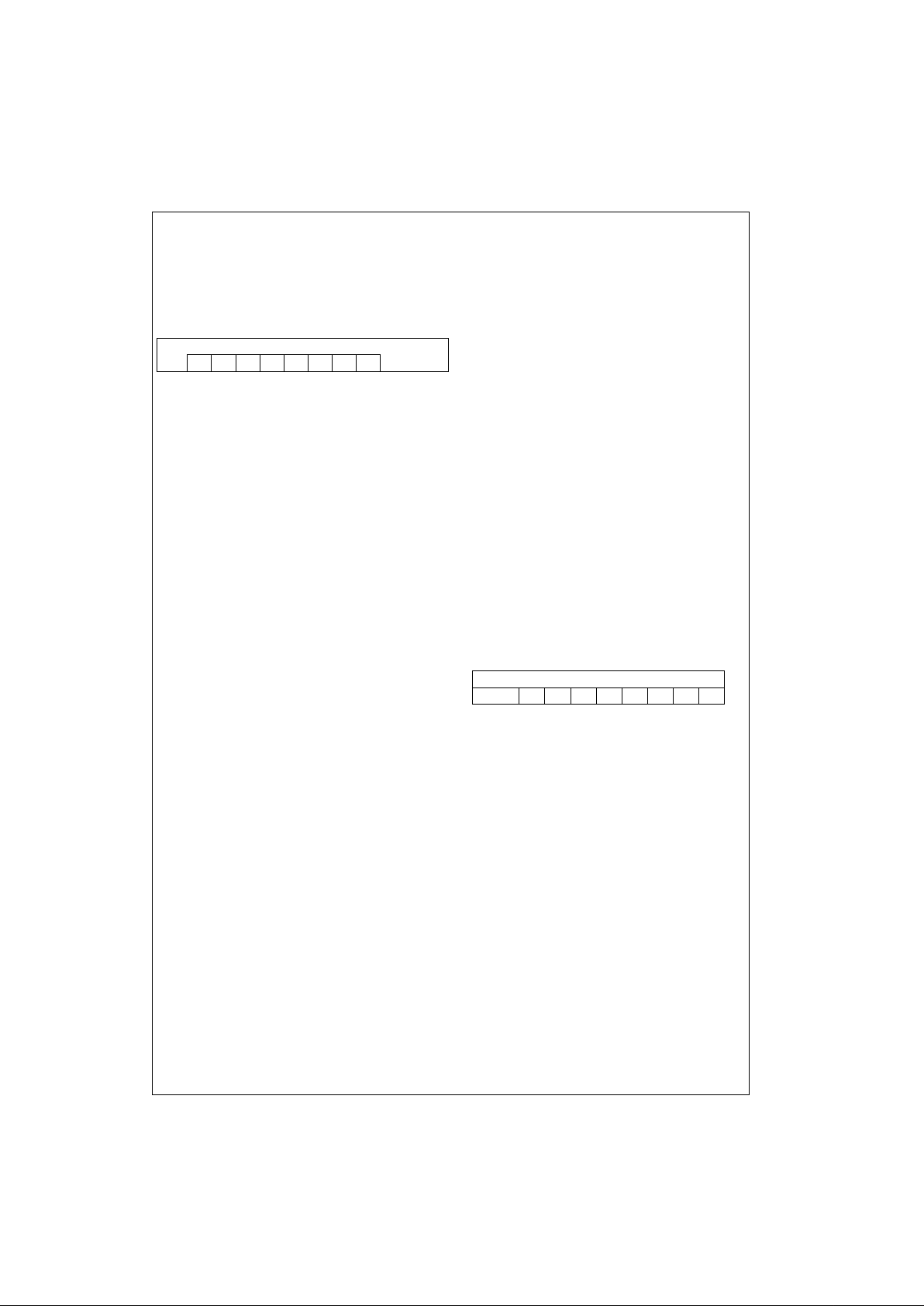
Idle state requires a 3-bit (110) sequence on TMS0. To provide correct 3-bit sequence on TMS0, the partial byte
would be written to the TMS0 shifter/buffer as:
A subsequent enable a nd load of CNT32 with decimal 3
and enable of the TMS0 shifter/buffer will initialize the shift
operation. Terminal count on CNT32 will complete the shift
operation. Since terminal count on CNT32 will c ause the
register selection to change within the shifter/buffer, the
values labeled as “x” will not be used an d are treated as
“don't cares”.
TDI SHIFTER/BUFFER
The TDI Shifter/Buffer block diagram is shown in Figure 13.
This block shifts in serial da ta fro m the TD I p ort a nd puts it
in parallel form for read ope rations at the PP I. During normal shift modes, d ouble-buffering i s achieved by configuring the shifter/buffer as a 2 x 8 FIFO. This block can also
be configured as a 16-bit Serial Signature Compactor
(SSC). Write, read, and shift ope rat ions a re co ntr ol led by a
local state machine that accepts stimulus from the PPI,
Mode Registers, CNT32 and the TCK Control section. The
TDI input always sh ifts in data on the rising edge of SC K.
The order of shifting is least significant bit first. The TDI
input includes a pull-up resi stor to force a logic 1 when the
test data signal returning from the scan chain is floating.
Read operations are complet ed if the shifter/buffer is not
empty and SSC mod e is not enabl ed. Otherwise they are
ignored. Write operations ar e only possible while in SSC
mode. Otherwise they are ignored.
Shifting occurs when the following conditions are all true:
• TDI is enabled with its respective mode bit.
• TDI shifter/buffer is not full.
• TCK is enabled according to the logic in TCK Control.
Local select circuitry is used to toggle back and forth
between the two regis ters of the “FIFO” when shifting. At
any given time, one register is selected for shift operations.
The other holds its previous sta te or can acce pt new seri al
data. Shift regis ter selection cha nges due to the following
two events:
• CNT3 in TCK Control signals that 8 bits have been
shifted in. This event is used for basic to ggling bet ween
each of the two shift registers.
• CNT32 enabled and at terminal count. This event is
used to account for scan lengths which are not multiples
of eight. When shift register selection changes due to
this signal, a partial byte (i.e., byte with
< eight valid da t a
bits shifted from the scan chain) will exist in the corresponding shift register. The embedded test software
functions written to support the evaluation of data read
from the TDI shifter/buffer must consider bit placement
when reading and evaluating a partial byte.
READING A PARTIAL BYTE FROM THE TDI SHIFTER/
BUFFER. Data is shifted from the scan chain into each TDI
register from most significant bit to least significant bit.
Consequently, the valid (i.e., meaningful) bits in a partia l
byte shifted into a TDI register will reside in t he upper significant bit locations. For example, if a scan operation
involves shifting and eva luating 53 bits returning to TDI,
TDI shifter/buffer must be r ead 7 times (i.e., 6 full bytes
plus a partial byte containing 5 meaningful bits). If the last 5
bits shifted back to the TDI shifter/buffer are 11010, then
upon completion of the shift operation (i.e ., terminal count
on CNT32), the sh ift register within the TDI shifter/buffer
will contain the following partial byte:
Following a read of a part ial byte, the embed ded test s oftware must adjust the position of the valid bits read from the
TDI shifter/buffer or th e position of the expected data to
assure that an accura te comparison is made ( an d th e nonmeaningful bits are masked).
MSB LSB
xxxxx011
→ TMS0
MSB LSB
TDI
→ 01011xxx
Page 14
www.fairchildsemi.com 14
SCANPSC100F
Serial Scan Interface (SSI) (Continued)
FIGURE 13. TDI Shifter/Buffer Block Diagram
FIGURE 14. TDI SSC Block Diagram
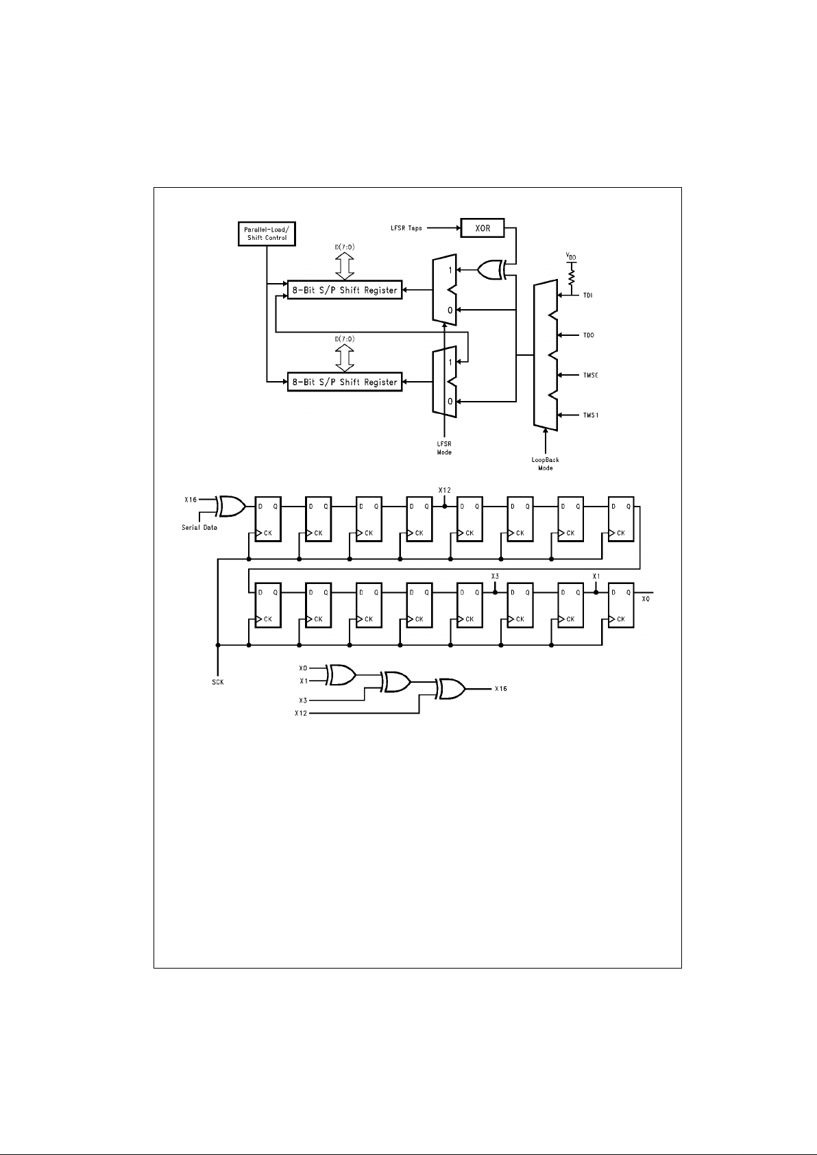
SSC MODE. By setting MODE1( 3), the TDI Sh ifter/Buffer
is reconfigured as a 16 -b i t S SC (Se ri al S ig nature Compactor) using the primitive polynomial:
F(X)
= X
16
+ X12 + X3 + X + 1
Within a chain of 1149.1 compliant devi ces, ther e are typically one or more input pins which are driven by uncontrolled signals (i.e., sign als which are not driven to known
logic levels during a boundary scan CAPTURE op eration).
These signals are mask ed during the evaluation of data
returning from the scan chain. The SSC within the PSC100
does not provide masking capabilities and, therefore, provides limited usefulne ss for bou nd ary scan test operations.
SSC mode may provi de usefulness in other seri al test or
non-test related implem ent atio ns w hich con t ain pred ictab l e
data returning into the TDI shifter/buffer.
Figure 14 shows a block diag ram of the Linear Feedb ack
Shift Register hookup.
The SSC is loaded by two PPI writes to the TDI ad dress.
When the SSC enable bit is set, a pulse is issued internally
that initializes the local parallel load logic such that the
SSC is loaded sequentially, most significant byte first, least
significant byte last. When in SSC mode, writes can be
completed at any time; however, shift operations will be
disabled until the SSC is fully lo aded. PPI reads from TDI
are ignored while in SSC mode.
Upon leaving SSC m ode an i nternal p ulse cau ses the TD I
shifter/buffer to be full. Also, local read select logic is initialized such that the signature is read most-significant byte
first.
TEST LOOP-BACK MODES. This feature provides a
means for testing SCANPSC100 functionality by looping
data appearing at t he output of an outgoing shif ter/buffer
(i.e., TMS0, TMS1 or TDO) back to the input of the TDI
shifter/buffer. The loop back function is accomplished with
a simple multiplexer (see Figure 13) whose path selection
is determined by setting the mode bits in MODE1(1:0).
Loop back does not disable TCK or prevent shifting of data
in the shifter/buffers to the scan chain(s) connected to the
PSC100. Therefore, the state and operation of the TAP
Page 15
15 www.fairchildsemi.com
SCANPSC100F
Serial Scan Interface (SSI) (Continued)
controllers within the scan chain(s) must be considered
when developing Loop-Back test vectors to prevent undesired shifting of data or TAP controller transitions wi thin the
scan chain.
32-BIT COUNTER (CNT32)
CNT32 is a 32-bit, count-down bi nary counter arranged in
four 8-bit segments . CNT32 can b e lo aded indepe ndent of
its enable/disable stat us. Loading requires four consecutive writes to its ad dr ess (least significant byte fi rst) . The s e
four writes must not be interleaved with writes to any other
address or the CNT32 write control logic will be re-initialized. This re-initialization will result in a partially filled
counter with an undesired value. CNT32 is reset each time
the counter hits terminal count or by asserting the RST
pin.
A synchronous reset conditi o n (se tting Mo de2 (1) ) d oes n ot
reset the counter and a new value must be written to
CNT32 to provide the desired number of TCK cycles.
SINGLE STEP MODE: All four 8-bit registers are rea dable
for testability; however, there are no update latches similar
to the ones used for the status bits. To stabilize the counter
for read operations during on-board test, the S ingle Step
Mode has been added. This allows the user to place
CNT32 in any state and then count for one SCK cycle (TCK
will not toggle when in singled step mode). The result can
then be read from the P PI. The counter can be tested by
loading it with values at its boundary conditions, and then
clocking for one cy cle to see t he results. For exam ple, the
counter could be loaded with the value:
00000001 00000000 00000000 00000000
The next step is to set the Single Step Mode bit so that the
counter counts down to the next st ate an d stops . The next
value is:
00000000 11111111 11111111 11111111
Four read cycles using the PPI will reveal the results of the
test.
Note: CNT3 2 will not wrap from t erminal count (i.e., 000 00000h decremented by 1 will re main unchanged and will not w rap to FFFFFFFFh).
Therefore, CNT32 should be loaded with a non-zero value prior to a Single
Step Mode Operation.
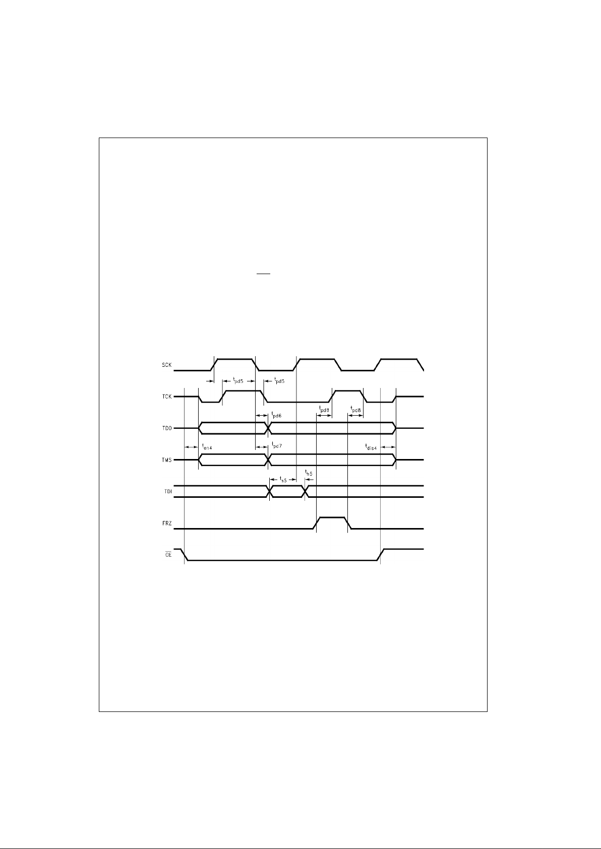
TIMING WAVEFORMS
FIGURE 15. Serial Scan Interface Timing
Embedded Test Software Support
A SCANPSC100 device driver is provided by Fairchild to
supply functions for perfo rming write , read an d shift op erations. Fairchild also offers a suite of software tools (ca lled
SCAN EASE) which enables ATPG or custom generat ed
test vectors to be embedded , appl ied an d evaluat ed w ithin
an IEEE 1149.1 compatible system. SCAN EASE is written
to run on a wide r ange o f pro cessor a nd me mo ry archi tectures. SCAN EASE includes the source code (ANSI C) and
is modular to allow user modification based on application
specific needs.
Page 16
www.fairchildsemi.com 16
SCANPSC100F
Application Note
SCK MINIMUM PULSE WIDTH CALCULATION
The SCANPSC100 Parallel to Serial Converter is intended
to act as the interface between a processor and an IEEE
1149.1 boundary scan chain. When used in this config uration, there is a critical timing situ ation that is no t obvious.
This timing involves the system clock rate at wh ich data
from the scan ring is bein g read into the SCANPSC100’s
TDI pin (target TAP controllers in SHIFT-DR or SHIFT-IR
states).
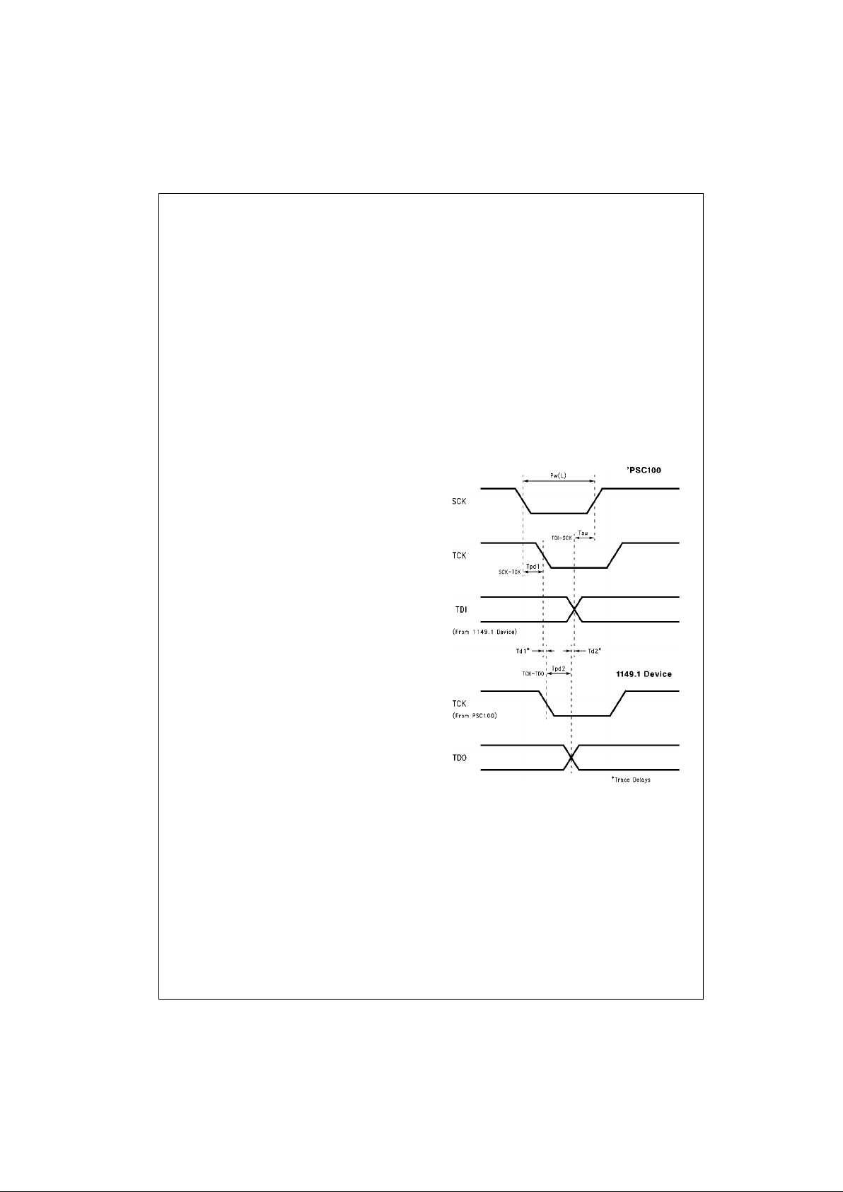
To fully understand the events which are taking place dur ing this critical pe riod , it i s usef ul to vi ew th e wave forms of
interest as they relat e in time. See Figure 16 . The TCK is
derived internally to th e SCANPSC100 based on the s ystem clock (SCK) and clock gating control. The result is that
when TCK is running, it is at the same frequency as SCK
but delayed in time by the SCK-TCK propagation delay.
The TCK signal from the SCANPSC100 drives all of the
IEEE 1149.1 target devices. On the rising edge of TCK,
data present at each scan cell is clocked into it. On the falling edge, this data is presente d at the output of the same
scan cell for the next adj acent cell to read. Wi th regard s to
the last cell in a particular target, the falling edge of TCK
presents the dat a in the last scan cell to the TDO pin, a
TCK-TDO propagation delay later.
At the SCANPSC100, data shifted in through the TDI pin is
clocked in on the rising edge of SCK, not TCK. The reason
for this is that TCK is generated internal to the
SCANPSC100 and in tended to control the boundary sca n
targets. The SCAN PSC1 00 is contr oll e d by S CK, th ere for e
the signal to be shi fted into the T DI pin needs to b e referenced to SCK not TCK. New TDI data mus t be present a
TDI-SCK set-up time prior to the rising ed ge of SCK in
order to guarantee valid i ty. Although SCK is usually contin uous, the TDI buffer is controlled by a SHIFT-ENABLE signal which is generated internal to the SCANPSC100,
based on the status of the TDI bu ffer and the Mode R egisters.
We now see the three major timing components which limit
the duration of the SCK pulse width low. There are two
minor additional dela ys which should be noted. The TCK
signal from the SCANPSC10 0 needs to arr ive at the target
device to be recognized , and this takes a finite amount of
time depending on the signal trace length a nd impedanc e.
Similarly, the TDO signal of the last target in the chain
needs to reach the TDI pi n of the SCANPSC1 00, taking a
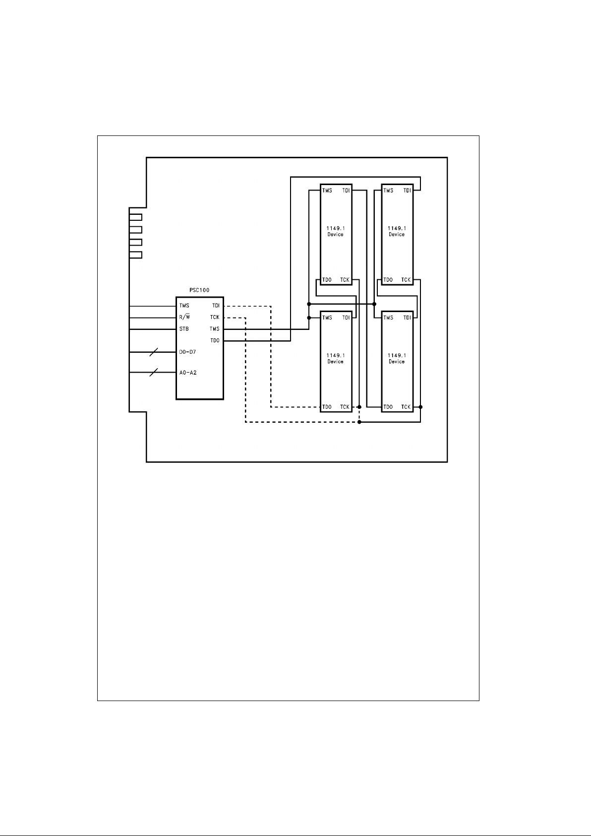
finite amount of time as w ell. These two trace de lays can
be minimized by making the ta rget device closest to the
SCANPSC100 the last device in the chain. See Figure 17.
PROGRAMMING RESTRICTIONS
Because certain mode bits enab le shift operation s for certain functions, these mode bits should not be changed
when shift operations are in progress. The alignment of all
registers during shift ope rations is co ntrolled by a three bit
counter in the TCK control block. Enabling or disabling a
function in the middle of a shift operation may disrup t the
logic necessary to keep all shifter /buffers byte -aligne d. For
example, if the TDO shifter/buffer (already loaded) is
enabled while the three bit counter value is three, the
shifter/buffer will only shift out 5 bits of the first byte loaded.
The following bits should not be changed when shift operations are in progres s, i.e., wh en TC K is enab led (see T CK
control section):
• MODE0(7:3)
• MODE1(4:3)
• MODE2(0)
Pw(L) minimum = t
PD1
+ tD1 + t
PD2
+ tD2 + t
SU
FIGURE 16. System Clock Timing
for Accurate TDI Data
Page 17
17 www.fairchildsemi.com
SCANPSC100F
PROGRAMMING RESTRICTIONS (Continued)
Note:- - - - - Minimize the lengths of thes e t w o t rac es.
FIGURE 17. SCANPSC100 Location Relative to Targets
Page 18
www.fairchildsemi.com 18
SCANPSC100F
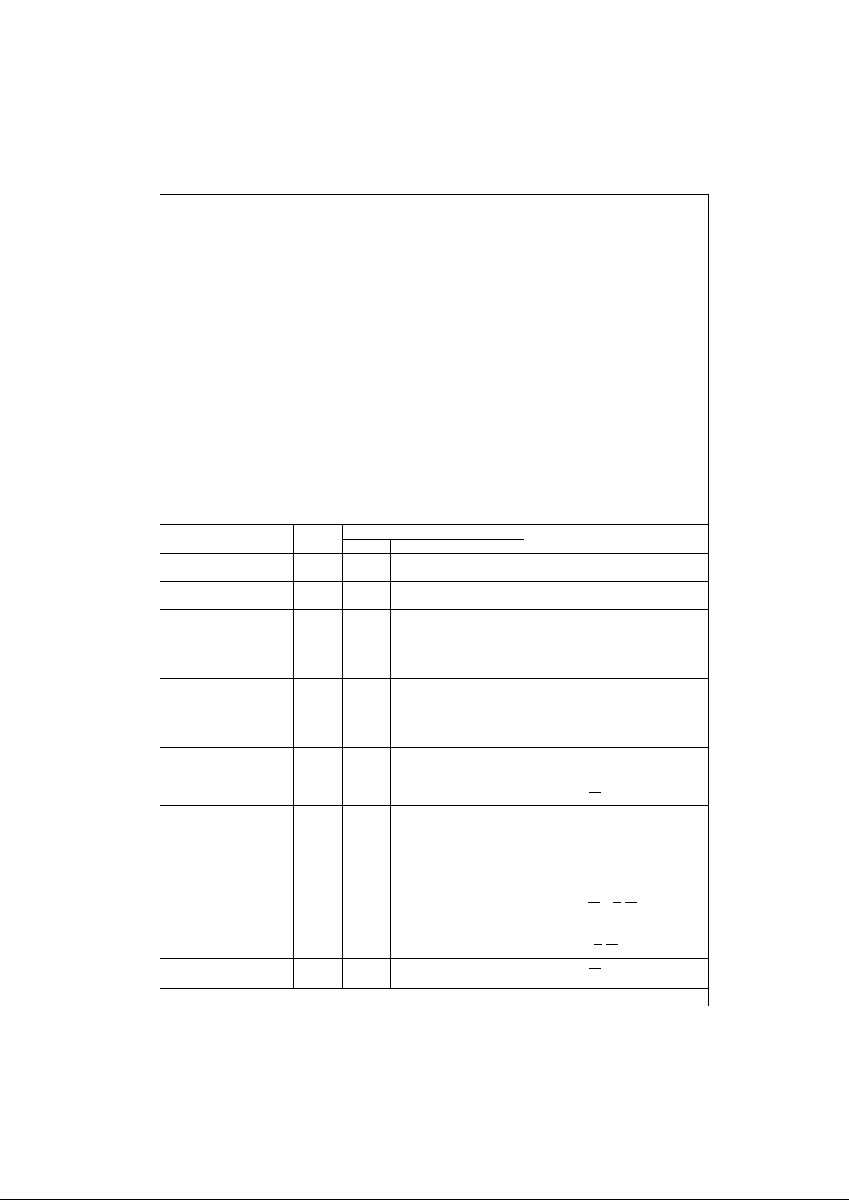
Absolute Maximum Ratings(Note 7) Recommended Operating
Conditions
Note 7: Absolute maximum ratings are those values beyond which damage
to the device may occur. The databook specifications should be met, without exception, to ensure that the system design is reliable over its power
supply, temperature, and ou tput/inp ut loadi ng varia bles. Fairchild does no t
recommend oper ation of SC AN o utside o f rec ommend ed o peratio n con ditions.
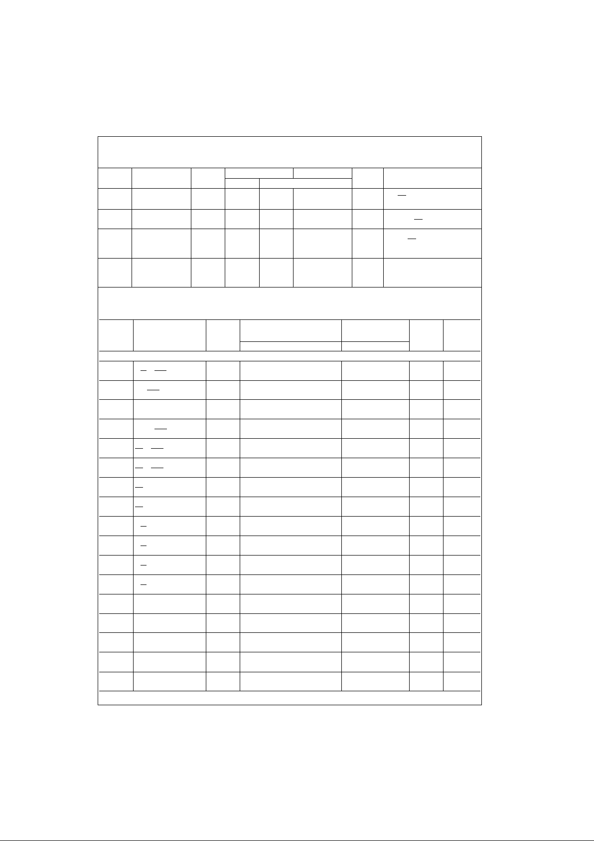
DC Electrical Characteristics
Supply Voltage (VCC) −0.5V to +7.0V
DC Input Diode Current (I
IK
)
V
I
= −0.5V −20 mA
V
I
= VCC + 0.5V +20 mA
DC Input Voltage (V
I
) −0.5V to VCC +0.5V
DC Output Diode Current (I
OK
)
V
O
= −0.5V −20 mA
V
O
= VCC + 0.5V +20 mA
DC Output Voltage (V
O
) −0.5V to VCC + 0.5V
DC Output Source/Sink Current (I
O
) ±50 mA
DC V
CC
or Ground Current ±50 mA
per Output Pin
DC Latchup Source or Sink Current
±300 mA
Junction Temperature
SOIC
+140°C
Storage Temperature
−65°C to +150°C
ESD Last Passing Voltage (Min) 4000V
Supply Voltage (V
CC
)
SCANPSC100F 4.5V to 5.5V
Input Voltage (V
I
) 0V to V
CC
Output Voltage (VO) 0V to V
CC
Operating Temperature (TA) −40°C to +85°C
Minimum Input Edge Rate
∆V/∆t
SCAN “F” Series Devices 125 mV/ns
V
IN
from 0.8V to 2.0V
V
CC
@ 4.5V, 5.5V
Symbol Parameter
V
CC
TA = +25°CTA = −40°C to +85°C
Units Conditions
(V) Typ Guaranteed Limits
V
IH
Minimum HIGH 4.5 2.0 2.0
V
V
OUT
= 0.1V or
Input Voltage 5.5 2.0 2.0 VCC − 0.1V
V
IL
Maximum LOW 4.5 0.8 0.8
V
V
OUT
= 0.1V or
Input Voltage 5.5 0.8 0.8 VCC − 0.1V
V
OH
Minimum HIGH 4.5 4.4 4.4
VI
OUT
= −50 µA
Output Voltage 5.5 5.4 5.4
4.5 3.86 3.76 VIN = VIL or V
IH
5.5 4.86 4.76 V IOH = −24 mA
All Outputs Loaded
V
OL
Maximum LOW 4.5 0.1 0.1
VI
OUT
= −50 µA
Output Voltage 5.5 0.1 0.1
4.5 0.36 0.44 VIN = VIL or V
IH
5.5 0.36 0.44 V IOL = 24 mA
All Outputs Loaded
I
IN
Maximum Input
5.5 ±0.1 ±1.0 µA
VIN = VCC for TDI, OE
Leakage Current VIN = VCC, GND for All Others
I
ILR
Maximum Input
5.5 −385 −385 µA
VIN = GND for
Leakage Current TDI, OE Only
I
OLD
Minimum V
OLD
= 1.65V Max
Dynamic 5.5 75 mA Maximum Test Duration = 2.0 ms,
Output Current One Output Loaded at a Time
I
OHD
Minimum V
OHD
= 3.85V Min
Dynamic 5.5 −75 mA Maximum Test Duration = 2.0 ms,
Output Current One Output Loaded at a Time
I
OZ
Maximum 3-STATE
±0.5 ±5.0 µA
VIN = VCC, GND
Leakage Current VIN (OE, R/W, CE, STB) = VIL, V
IH
I
OZT
Maximum I/O VIN = VCC, GND
Leakage Current ±0.6 ±6.0 µAVO = VCC, GND
VIN(R/W, CE, STB) = VIL, V
IH
I
CC
Maximum Quiescent
5.5 8 80 µA TDI, OE Float
Supply Current
Page 19
19 www.fairchildsemi.com
SCANPSC100F
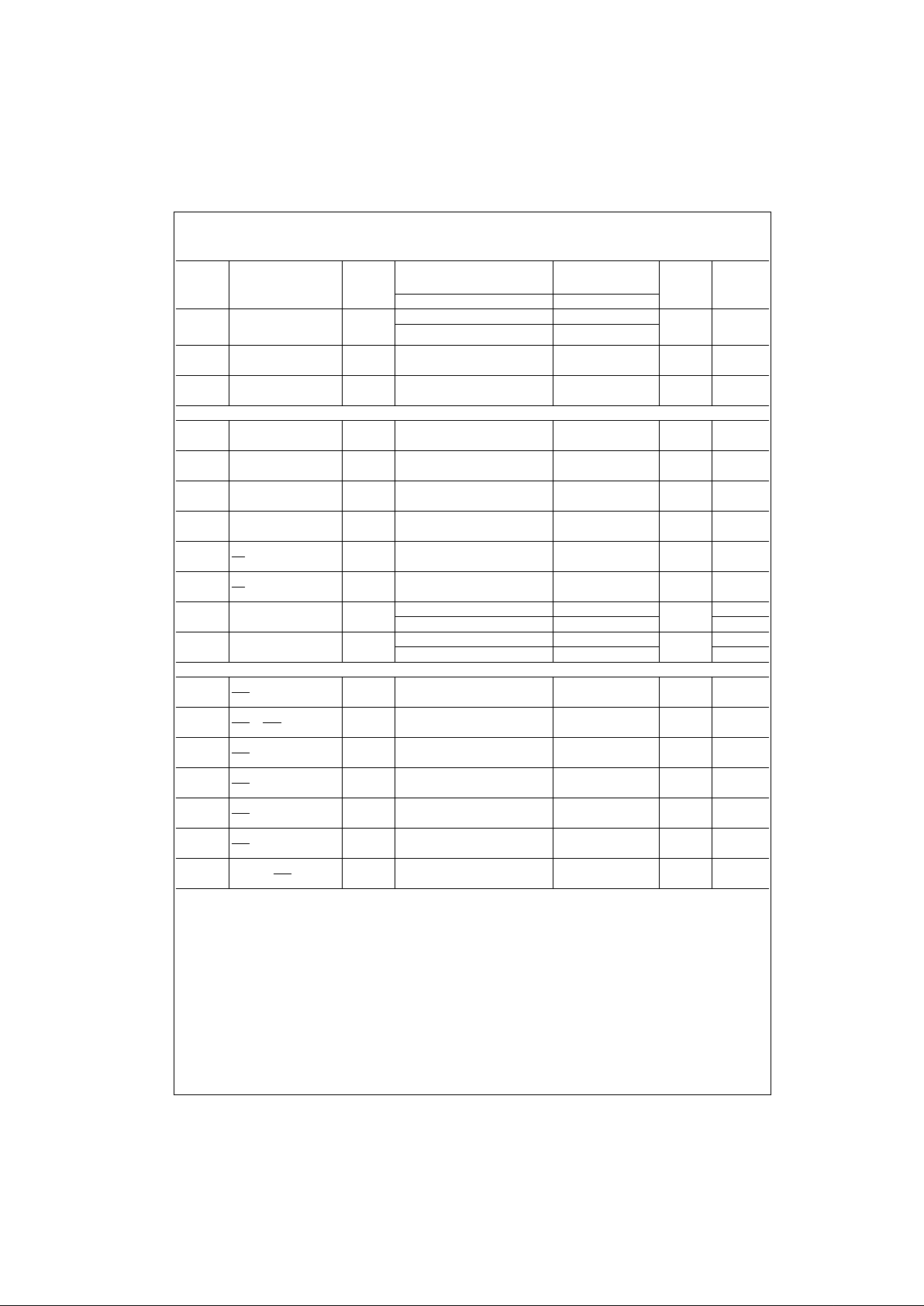
DC Electrical Characteristics (Continued)
Note 8: This parameter is not direct ly t es t able, but is derived for use in Total Power Supply calculations.
AC Electrical Characteristics/Operating Requirements
Symbol Parameter
V
CC
TA = +25°CTA = −40°C to +85°C
Units Conditions
(V) Typ Guaranteed Limits
I
CCMAX
Maximum Quiescent
5.5 768 840 µA TDI, OE
LOW
Supply Current
I
CCT
Maximum
5.5 0.6 1.50 mA
VIN = VCC − 2.1V
I
CC
/Input Float: TDI, OE
I
CCTR
Maximum VIN = VCC −2.1V
I
CC
/Input 5.5 0.65 1.65 mA TDI and OE Only
Float Untested Pin
I
CCD
Dynamic Power mA/ VIH = VCC, VIL = 0,
Supply Current 5.5 1.70 2.30 2.30 MHz V
CC
= Max, Outputs Open,
(Note 8) F
SCK
= 25 MHz
Symbol Parameter
V
CC
TA = +25°CT
A
= −40°C to +85°C
Units
Figure
(V)
CL = 50 pF CL = 50 pF
Number
(Note 9) Min Typ Max Min Max
PARALLEL PROCESSOR INTERFACE (PPI)
t
PD1
Prop Delay
5.0 5.0 14.0 19.5 5.0 24.0 ns
Figures 2, 3,
4
R/W
to RDY
t
PD2
Prop Delay
5.0 5.0 14.0 19.5 5.0 24.0 ns Figures 2, 3
A to RDY
t
PD3
Prop Delay
5.0 5.0 14.0 19.5 5.0 24.0 ns Figure 3
A to D
t
PD4
Prop Delay
5.0 8.0 14.5 19.0 8.0 20.5 ns
Figures 2, 3,
4, 6
STB to RDY
t
EN1
Enable Time
5.0 2.0 7.0 10.0 2.0 11.0 ns Figures 2, 3
CE
to RDY
t
DIS1
Disable Time
5.0 1.0 5.5 8.0 1.0 9.0 ns Figures 2, 3
CE to RDY
t
EN2
Enable Time
5.0 3.0 9.5 13.5 3.0 14.5 ns Figure 3
CE
to D
t
DIS2
Disable Time
5.0 2.5 7.5 11.0 2.5 12.0 ns Figure 3
CE
to D
t
EN3
Enable Time
5.0 3.0 10.0 14.0 3.0 15.0 ns Figure 3
R/W to D
t
DIS3
Disable Time
5.0 3.0 8.5 12.5 3.0 13.5 ns Figure 3
R/W to D
t
H1
Hold Time,
5.0 0.5 0.0 0.5 ns
Figures 2, 3,
4, 6
R/W to STB
t
S1
Setup Time
5.0 1.0 0.0 1.0 ns
Figures 2, 3,
4, 6
R/W to STB
t
H2
Hold Time,
5.0 4.0 2.5 4.0 ns Figures 2, 3
A to STB ↑
t
S2
Setup Time,
5.0 4.0 1.5 4.0 ns Figures 2, 3
A to STB ↑
t
H3
Hold Time,
5.0 4.0 2.5 4.0 ns Figure 2
D to STB ↑
t
S3
Setup Time,
5.0 0.0 −2.0 0.0 ns Figure 2
D to STB ↑
t
S4
Setup Time,
5.0 7.0 5.0 7.0 ns
Figures 4, 5,
6, 7
STB ↑ to SCK ↓
Page 20
www.fairchildsemi.com 20
SCANPSC100F
AC Electrical Characteristics/Operating Requirements (Continued)
Note 9: Voltage Range 5.0 is 5.0V ± 0.5V.
Note 10: SSC Mode
Symbol Parameter
V
CC
TA = +25°CT
A
= −40°C to +85°C
Units
Figure
(V)
CL = 50 pF CL = 50 pF
Number
(Note 9) Min Typ Max Min Max
t
W
Clock Pulse Width
SCK (L)
SCK (H)
5.0 19.5 12.0 19.5
ns Figures 4, 6
18.5 14.0 18.5
t
W1
Pulse Width
5.0 5.5 2.0 5.5 ns Figures 4, 6
STB (H or L)
f
MAX
Maximum
5.0 25 35 25 MHz
Frequency Clock
SERIAL SCAN INTERFACE (SSI)
t
PD5
Prop Delay
5.0 3.0 8.0 11.0 3.0 12.0 ns Figure 15
SCK to TCK
t
PD6
Prop Delay
5.0 5.5 12.0 16.0 5.5 17.5 ns Figure 15
SCK to TDO
t
PD7
Prop Delay
5.0 4.5 11.0 14.5 4.5 15.5 ns Figure 15
SCK to TMS
t
PD8
Prop Delay
5.0 3.0 8.0 10.5 3.0 11.5 ns Figure 15
FRZ to TCK
t
EN4
Enable Time
5.0 2.0 7.0 10.0 2.0 11.0 ns Figure 14
OE to JTAG
t
DIS4
Disable Time
5.0 1.0 6.0 9.0 1.0 10.0 ns Figure 14
OE
to JTAG
t
H5
Hold Time, H or L 5.0 0.5 −1.5 0.5
ns
Figure 15
TDI to SCK (Note 10) 0.0 −2.0 0.0 Figure 15
t
S5
Setup Time, H or L 5.0 5.0 3.0 5.0
ns
Figure 15
TDI to SCK (Note 10) 6.5 3.5 6.5 Figure 15
RST RELATED TIMING
t
PD
Prop Delay
5.0 8.0 17.5 24.0 8.0 25.5 ns
RST to D
t
PD
Prop Delay
5.0 8.0 19.5 25.5 8.0 28.0 ns
RST
to RDY
t
PHL
Prop Delay
5.0 7.0 16.5 24.5 7.0 24.5 ns
RST
to INT
t
PLH
Prop Delay
5.0 5.5 12.5 17.0 5.5 18.5 ns
RST to TDO
t
PLH
Prop Delay
5.0 5.5 12.0 16.0 5.5 17.5 ns
RST
to TMS
t
WR
Pulse Width
5.0 6.0 4.0 6.0 ns
RST (L)
t
REC
Recovery Time 5.0 1.0 −0.5 1.0 ns
SCK from RST
Page 21
21 www.fairchildsemi.com
SCANPSC100F Embedded Boundary Scan Controller (IEEE 1149.1 Support)
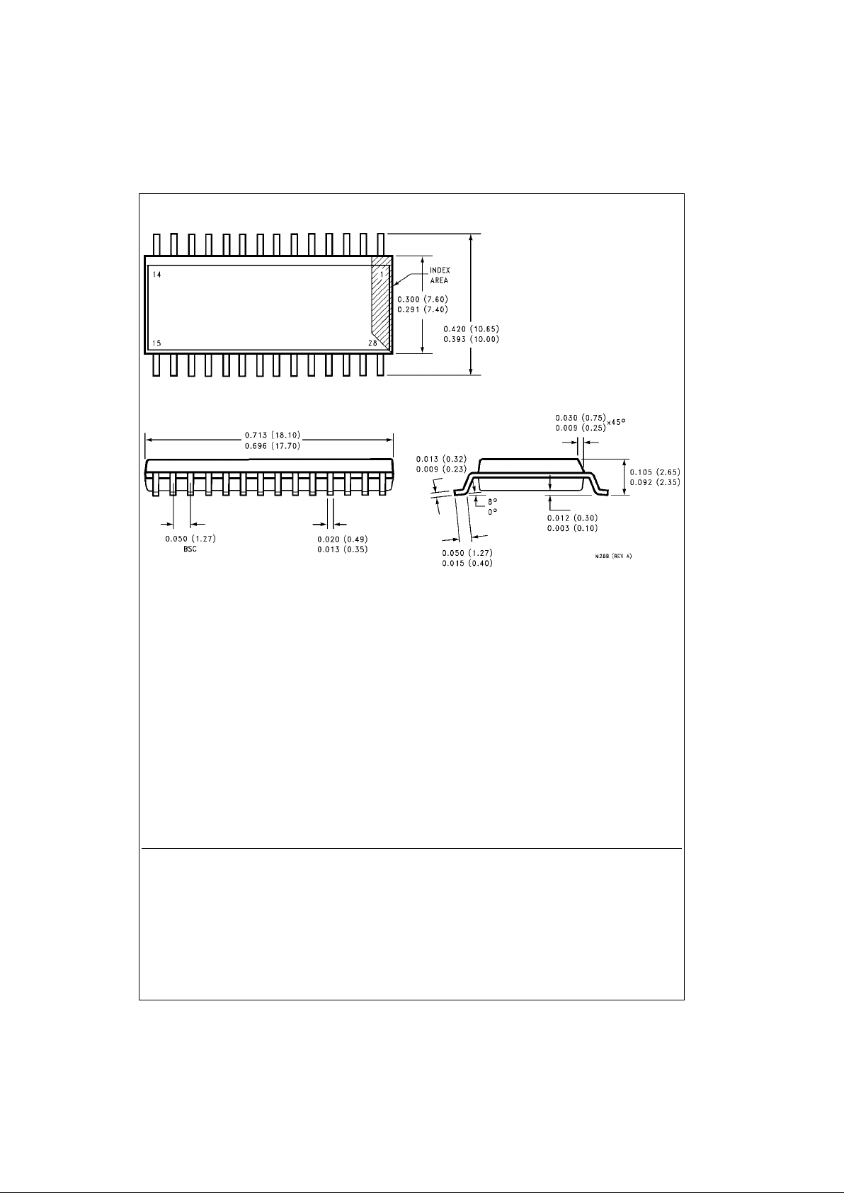
Physical Dimensions inches (millimeters) unless otherwise noted
28-Lead Small Outline Integrated Circuit (SOIC), JEDEC MS-013, 0.300 Wide
Package Number M28B
Fairchild does not assume any responsibility for use of any circuitry described , no circuit patent licenses are implied and
Fairchild reserves the right at any time without notice to change said circuitry and specifications.
LIFE SUPPORT POLICY
FAIRCHILD’S PRODUCTS ARE NOT AUTHORIZED FOR USE AS CRITICAL COMPONENTS IN LIFE SUPPORT
DEVICES OR SYSTEMS WITHOUT THE EXPRESS WRITTEN APPROVAL OF THE PRESIDENT OF FAIRCHILD
SEMICONDUCTOR CORPORATION. As used herein:
1. Life support devices or systems are dev ic es or syste ms
which, (a) are intended for surgical implant into the
body, or (b) support or sustain life, and (c) whose failure
to perform when properly used in accordance with
instructions for use provide d in the labe l ing, can be re asonably expected to result in a significant injury to the
user.
2. A critical compo nent in any com ponen t of a life s upp ort
device or system whose failure to perform can be reasonably expected to cause the failure of the l ife support
device or system, or to affect its safety or effectiveness.
www.fairchildsemi.com
 Loading...