

Page 1

March 1993
Revised August 2000
SCANPSC110F
SCAN Bridge Hierarchical and Multidrop Addressable
JTAG Port (IEEE1149. 1 System Test Support)
Support)
SCANPSC110F SCAN Bridge Hierarchical and Multidrop Addressable JTAG Port (IEEE1149.1 System Test
General Description
The SCANPSC110F Bridge extends the IEEE St d. 1149.1
test bus into a multidrop test bu s env ironme nt. The adva ntage of a hierarchical approa ch over a single serial scan
chain is improved test throughput and the ability to r emove
a board from the system and retain test access to the
remaining modules. Each SCANPSC110F Bridge supports
up to 3 local scan rings which can be accessed individually
or combined serially. Addressing is accomp lished by loading the instruction register with a value matching that of the
Slot inputs. Backplane and in ter-board testing can easily
be accomplished by par king the local TAP Controllers in
one of the stable TAP Controller state s via a Park instru ction. The 32-bit TC K coun ter en ables built in self te st o pe rations to be performed on one port while other scan chains
are simultaneously tested.
Features
■ True IEEE1149.1 hierarchical and multidrop addressable
capability
■ The 6 slot inputs support up to 59 unique addresses, a
Broadcast Address, and 4 Multi-cast Group Addresses
■ 3 IEEE 1149.1- compatible configurable local scan ports
■ Mode Register allows local TAPs to be bypassed,
selected for insertion into the scan chain in dividually, or
serially in groups of two or three
■ 32-bit TCK counter
■ 16-bit LFSR Signature Compactor
■ L4
■ local TAPs can be 3-stated via the OE
alternate test master to take control of the local TAPs
input to allow an
Ordering Code:
Order Number Package Number Package Description
SCANPSC110FSC M28B 28-Lead Small Outline Integrated Circuit (SOIC), JEDEC MS-013, 0.300 Wide
Devices also availab le in Tape and Reel. Specify by appending the suffix letter “X” to the o rdering code.
Connection Diagram Pin Descriptions
Names
TCK
TMS
TDI
TDO
TRST
S
(0,5)
OE
TCK
TMS
TDI
TDO
Pin
Backplane Test Clock Input
B
Backplane Test Mode Select Input
B
Backplane Test Data Input
B
Backplane Test Data Output
B
Asynchronous Test Reset Input (Active LOW)
Address Select Port
Local Scan Port Output Enable (Active LOW)
Local Port Test Clock Output
L(1–3)
Local Port Test Mode Select Output
L(1–3)
Local Port Test Data Input
L(1–3)
Local Port Test Data Output
L(1–3)
Description
© 2000 Fairchild Semiconductor Corporation DS011570 www.fairchildsemi.com
Page 2

TABLE 1. Glossary of Terms
LFSR Linear Feedback Shift Register. When enabled, will generate a 16-bit signature of sampled serial test
data.
LSP Local Scan Port. A four signal port that drives a “local” (i.e. non-backplane) scan chain.
(e.g., TCK
, TMSL1, TDOL1, TDIL1)
L1
Local Local is used to describe IEEE Std. 1149.1 compliant scan rings and the SCANPSC110F Bridge Test
SCANPSC110F
Access Port that drives them. The term “local” was adopted from the system test architecture that the
SCANPSC110F Bridge will most commonly be used in; namely, a system test backplane with a
SCANPSC110F Bridge on each card driving up to 3 “local” scan rings per card. (Each card can contain
multiple SCANPSC110Fs, with 3 local scan ports per SCANPSC110F.)
Park/Unpark Park, parked, unpark, and unparked, are used to describe the state of the LSP controller and the state
of the local TAP controllers (the “local TAP controllers” refers to the TAP controllers of the scan components that make up a local scan ring). Park is also used to describe the action of parking a LSP (transitioning into one of the Parked LSP controller states). It is important to understand that when a LSP
controller is in one of the parked states, TMS
TAP controllers in a given state.
is held constant, thereby holding or “parking” the local
L
TAP Test Access Port as defined by IEEE Std. 1149.1
Selected/Unselected Selected and Unselected refers to the state of the SCANPSC110F Bridge Selection Controller. A
selected SCANPSC110F has been properly addressed and is ready to receive Level 2 protocol. Unselected SCANPSC110Fs monitor the system test backplane, but do not accept Level 2 protocol (except
for the GOTOWAIT instruction). The data registers and LSPs of unselected SCANPSC110Fs are not
accessible from the system test master.
Active Scan Chain The Active Scan Chain refers to the scan chain configuration as seen by the test master at a given
moment. When a SCANPSC110F is selected with all of its LSPs parked, the active scan chain is the
current scan bridge register only. When a LSP is unparked, the active scan chain becomes: TDI
current SCANPSC1 10F registe r
for Unparked configurations of the LSP network.
→ the local s ca n r i ng re g ist e r s → a PAD bit → TDO
. Refer to Table 4
B
Level 1 Protocol Level 1 is the protocol used to address a SCANPSC110F.
Level 2 Protocol Level 2 is the protocol that is used once a SCANPSC110F is selected. Level 2 protocol is IEEE Std.
1149.1 compliant when an individual SCANPSC110F is selected.
PAD A one bit register that is placed at the end of each local scan port scan-chain. The PAD bit eliminates
the prop delay that would be added by the SCANPSC110F LSPN logic between TDI
or TDO
by buffering and synchronizing the TDIL inputs to the falling edge of TCKB, thus allowing data
B
to be scanned at higher frequencies without violating set-up and hold times.
and TDO
Ln
LSB Least Significant Bit, the right-most position in a register (bit 0)
MSB Most Significant Bit, the left-most position in a register
→ the
B
L(n+1)
www.fairchildsemi.com 2
Page 3

TABLE 2. Detailed Pin Description Table
Name I/O (Note 1)
TMS
TTL Input w/Pull-Up Resistor 10 BACKPLANE TEST MODE SELECT: Controls sequencing
B
Pin #
(SOIC & LCC)
through the TAP Controller of the SCANPSC110F Bridge. Also
controls sequencing of the TAPs which are on the three (3) local
scan chains.
TDI
TDO
TTL Input w/Pull-Up Resistor 12 BACKPLANE TEST DATA INPUT: All backplane scan data is
B
3-STATEable, 13 BACKPLANE TEST DATA OUTPUT: This output drives test data
B
32 mA/64 mA Drive,
Reduced-Swing,
supplied to the SCANPSC110F through this input pin.
from the SCANPSC110F and the local TAPs, back toward the scan
master controller.
Output
TCK
TTL Schmitt Trigger Input 11 TEST CLOCK INPUT FROM THE BACKPLANE: This is the mas-
B
ter clock signal that controls all scan operations of the
SCANPSC110F and of the three (3) local scan ports.
TRST
TTL Input w/Pull-Up Resistor 9 TEST RESET: An asynchronous reset signal (active LOW) which
initializes the SCANPSC110F logic.
S
OE
(0–5)
TTL Inputs 2, 3, 4, SLOT IDENTIFICATION: The configuration of these six (6) pins is
5, 6, 7
used to identify (assign a unique address to) each SCANPSC110F
on the system backplane.
TTL Input 1 OUTPUT ENABLE for the Local Sca n Ports, acti ve LOW. When
HIGH, this active-LOW control signal 3-STATEs all three local scan
ports on the SCANPSC110F, to enable an alternate resource to
access one or more of the three (3) local scan chains.
TDO
3-STATEable, 15,19, TEST DATA OUTPUTS: Individual output for each of the three (3)
L(1–3)
24 mA/24 mA 24
local scan ports.
Drive Outputs
TDI
TMS
TCK
V
CC
TTL Inputs w/Pull-Up 18, 23, TEST DATA INPUTS: Individual scan data input for each of the
L(1–3)
Resistors 27
3-STATE able, 16, 20, TEST MODE SELECT OUTPUT S: Individual output for each of the
L(1–3)
24 mA/24 mA 25
Drive Outputs
3-STATE able, 17, 22, LOCAL TEST CLOCK OUTPUTS: Individual output for each of
L(1–3)
24 mA/24 mA 26
Drive Output
three (3) local scan ports.
three (3) local scan ports. TMS
(which is assumed to be present on a connected TMS input, per
the IEEE 1149.1 requirement)
the three (3) local scan ports. These are buffered versions of
TCK
.
B
Power Supply Voltage 8, 28 Power supply pins, 5.0V ±10%.
GND Ground potential 14, 21 Power supply pins 0V.
Note 1: All pins are active HIGH unless otherwise note d.
Description
does not provide a pu ll- up re sis tor
L
SCANPSC110F
3 www.fairchildsemi.com
Page 4

Overview of SCANPSC110F Bridge Functions
SCANPSC110F
FIGURE 1. SCANPSC110F Bridge Architecture
SCANPSC110F BRIDGE ARCHITECTURE
Figure 1 shows the basic architecture of the
SCANPSC110F. The device’s major functional blocks are
illustrated here. The TAP Controller, a 16-state state
machine, is the central contro l for the device. Th e instruction register and various test data registers can be scanned
to exercise the various functions of the SCANPSC110F
(these registers behave as defined in IEEE Std. 1149.1).
The SCANPSC110F selection controller pr ovides th e functionality that allows the 1149.1 protocol to be used in a
multi-drop environm ent. It primarily com pares the address
input to the slot identification and enables the
SCANPSC110F for subsequent scan operations.
The Local Scan Port Network (LSPN) contains multiplexing
logic used to select different port configurations. The LSPN
control block contains the Local Scan Port Controllers
(LSPC) for each Local Scan Port (LSP
This control block receives i nput from the SCANPSC 110F
instruction register, mode register, and the TAP controller.
Each local port contain s all four ( 4) bounda ry scan signals
needed to interface with the local TAPs.
www.fairchildsemi.com 4
, LSP2, and LSP3).
1
SCANPSC110F BRIDGE STATE MACHINES
The SCANPSC110F is IEEE 1149.1-compatible, in that it
supports all required 1149.1 operations. In additi on, it supports a higher level of prot ocol, (Leve l 1), th at extends the
IEEE 1149.1 Std. to a multi-drop environment.
In multi-drop scan systems, a sca n tester can select individual SCANPSC110Fs for participation in upc oming scan
operations. SCANPSC110F “selection” is accomplished by
simultaneously scanning a d evice address out to multiple
SCANPSC110Fs. Through an on-chip address matching
process, only those SCANPSC110Fs whose staticallyassigned address matches the scanned-out address
become selected to receive further instructions from the
scan tester. SCANPSC110F selection is done using a
“Level-1” protocol, while follow-on instructions are sent to
selected SCANPSC110Fs by using a “Level-2” protocol.
Page 5

Overview of SCANPSC110F Bridge Functions (Continued)
FIGURE 2. SCANPSC110F Bridge State Machines
The SCANPSC110F contains three distinct but coupled
state-machines (see Figure 2). The first of these is the
TAP-control state-machine, which is used to drive the
SCANPSC110Fs scan ports in conformance with the
1149.1 Standard (see Figure 17 of appendix). The seco nd
is the SCANPSC110F-selection state -machine (Figure 3).
The third state-mach ine actual ly consist s of three identical
but independent sta te-machines (see Figure 4), o ne per
SCANPSC110F local scan port. Each of these scan portselection state-machin es allow s individ ual lo cal ports to be
inserted into and remov ed from th e SCANPSC 110Fs overall scan chain.
The SCANPSC110F selection state-machi ne performs the
address matching which gives the SCANPSC110F its
multi-drop capability. That logic supports singleSCANPSC110F access, multi-cast, and broadcast. The
SCANPSC110F-selection state-machine implements the
chip’s Level-1 protocol.
SCANPSC110F
KEY
+ = OR
& = AND
ADDR = 6-bit address in the Ins t ruc t ion Register
SLOT = Static addr es s in t he SCANPSC110F Selection Controller
FIGURE 3. State Machine for SCANPSC110F Bridge Selection Controller
5 www.fairchildsemi.com
Page 6

Overview of SCANPSC110F Bridge Functions (Continued)
SCANPSC110F
FIGURE 4. Local SCANPSC110F Bridge Port Configuration State Machine
The SCANPSC110F’s scan port-configuration statemachine is used to control the insertion o f local scan ports
into the overall scan chai n, or the isolation of local ports
from the chain. From th e pe rsp ective of a syste m’s (single )
scan controller, each SCANPSC110F presents only one
scan chain to the m ast er. The SCANPSC110F architectur e
allows one or more of th e SCANPSC110F’s local ports to
be included in the active scan chain.
Each local port can be “parked” in one of four stab le stat es
(Parked-TLR, Parked-RTI, Parked-Pause-DR or ParkedPause-IR), either individually or simultaneously with o ther
local ports. Parking a chain remove s that local chain from
the active scan chain. Conver sely, a parked chain can be
“unparked”, causing the corresponding local port to be
inserted into the active scan chain.
As shown in Figure 4, the SCANPSC110F's three scan
port-configuration state-machines allow each of the part's
local ports to occupy a different state at any given time. For
example, some ports m ay be parked, perhaps in differe nt
states, while other ports participate in scan operations. The
state-diagram shows that some state transitions depend on
the current state of the TAP-control state-ma chine. As an
example, a local port which is presently in the Parked-RTI
state does not beco me unpa rked (i.e., enter the Unparked
state) until the SCANPSC110F receives an UNPARK
instruction and the SCANPSC110F's TAP state-machine
enters the Run-Test/Idle state.
Similarly, certain transitions of the scan port-configuratio n
state-machine can force the SCANPSC110F's TAP-control
state-machine into sp ecific states. For example, when a
local port is in the Unparked state a nd the SCA NPSC 110F
receives a PARKRTI instruction, the Local Port controller
enters the Parked-RTI state in which TMS
LOW until the port is later unparked. While TMS
LOW, all devices on that local scan chain remain in thei r
current TAP State (the RTI TAP controller state in this
example).
The SCANPSC110F's scan port-configuration statemachine implemen ts part of the SC ANPSC110F's Level-2
protocol. In additio n, the SCANPSC110F provides a number of Level-2 instructions for functions other than local
scan port configuratio n. These in structions provide a ccess
to and control of various registers within the
SCANPSC110F. This set instructions includes:
BYPASS CNTRSEL
EXTEST LFSRON
SAMPLE/PRELOAD LFSROFF
IDCODE CNTRON
MODESEL CNTROFF
MCGRSEL GOTOWAIT
LFSRSEL
Figure 5 illustrates how the SCANPSC110F's statemachines interact. The SCANPSC110F-selection statemachine enables or d isables operation of th e chip's three
port-selection state-machines. In SCANPSC110Fs which
are selected via Level-1 protocol (either as individual
SCANPSC110Fs or as members of broadcast or multi- cast
groups), Level-2 proto col commands can be used to park
or unpark local scan ports. Note that most transitions of the
port-configuration state-machines are gated by particular
states of the SCANPS C110F's TAP-control state-machine,
as shown in Figures 4, 5.
will be held
Ln
is held
Ln
www.fairchildsemi.com 6
Page 7

Overview of SCANPSC110F Bridge Functions (Continued)
SCANPSC110F
FIGURE 5. Relationship Between SCANPSC110F Bridge State Machines
Following a hardware reset, the TAP controller statemachine is in the Test-Logic-Reset (TLR) state; the
SCANPSC110F-selection state-machine is in the Wait-For-
Address state; and each of the three por t-selection statemachines is in the Parked-TLR stat e. The SCAN PSC110F
is then ready to receive Level-1 protocol, followed by Level2 protocol.
Tester/SCANPSC110F
Bridge Interface
An IEEE 1149.1 system tester sends instructions to a
SCANPSC110F via that SCANPSC110F’s backplane scanport. Following test logic reset, the SCANPSC110F’s selec-
tion state-machine is in the Wait-For-Address state. When
the SCANPSC110F’s TAP controller is sequenced to the
Shift-IR state, data shifted in through the TDI
shifted into the SCANPSC110F’s instruction register. Note
that prior to successful se lectio n o f a S CAN PSC110F, data
is not shifted out of the instruction register and out through
the SCANPSC110F’s TDO
scan operations. Instead, as each new bit enters the
instruction register’s most-significant bit, data shifted out
from the least-significant bit is discarded.
output, as it is duri ng normal
B
input is
B
When the instruc tion register is u pdated with the address
data, the SCANPSC110F’s address-recognition logic co mpares the six least-sign i fican t bits of the instruction reg i ster
with the 6-bit assig ned address which is statically pre sent
on the S
address is compared with the reserved Broadcast and
Multi-cast addresses. If an ad dress match is detecte d, the
SCANPSC110F-selection state-machine ente rs one of the
two selected states. If the scanned address does not match
a valid single-slot address or one of the reserved broadcast/multi-cast addresses, the SCANPSC110F-selection
state-machine enters the Unselected state.
Note that the SLOT inputs sho ul d not be set to a value corresponding to a multi-cast group, or to the broadcast
address. Also note that the single-SCANPSC110F selection process must be performed for all SCANPSC110Fs
which are subsequently to be addressed in multi-cast
mode. This is requi red because each such device’s Multicast Group Register (MC GR) must be prog rammed with a
multi-cast group n umber, and the MCG R is n ot accessibl e
to the test controller until that SCANPSC110F has first
entered the Selected-Single-SCANPSC110F state.
Once a SCANPSC110F has been selected, L evel-2 pro tocol is used to issue commands an d to access the chip’s
various registers.
7 www.fairchildsemi.com
inputs. Simultaneously, the scanned-in
(0–5)
Page 8

Tester/SCANPSC110FBridge Interface (Continued)
Register Set
The SCANPSC110F Bridge includes a number of re gisters
which are used for SC ANPSC110F selection and configuration, scan data manipulation, and scan -support opera-
SCANPSC110F
tions. These registers can be grouped as shown in Table 3.
The specific fields and functio ns of each of these re gisters
are detailed in the section of this document titled “Data
Register Descriptions”.
TABLE 3. Registers
Register Name BSDL Name Description
Instruction Register INSTRUCTION SCANPSC110F addressing and instruction-decode
Boundary-Scan Register BOUNDARY IEEE Std. 1149.1 required register
Bypass Register BYPASS IEEE Std. 1149.1 required register
Device Identification Register IDCODE IEEE Std. 1149.1 optional register
Multi-Cast Group Register MCGR SCANPSC110F-group address assignment
Mode Register MODE SCANPSC110F local-port configuration and control bits
Linear-Feedback Shift Register LFSR SCANPSC110F scan-data compaction (signature gen er ation )
TCK Counter Register CNTR Local-port TCK clock-gating (for BIST)
Note that when any of these registe rs is sele cted for inse rtion into the SCANPSC110F's scan-chain, scan data
enters through t hat r egister's most- sign ificant b it. Similar ly,
data that is shifted out of the register is fed to the scan
input of the next-downstream device in the scan-chain.
IEEE Std. 1149.1 required register
Addressing Scheme
The SCANPSC110F Bridge architectur e extends the fun ctionality of the IEEE 1149.1 Standard by supplementing
that protocol w ith an addressing scheme whic h allows a
test controller to communicate with specific
SCANPSC110Fs within a network of SCANPSC110Fs.
That network can include both m ulti-drop an d hierarchical
connectivity. In effect, the SCANPSC110F architecture
allows a test controller to dynamically select sp ecific portions of such a network for participation in scan operations.
This allows a complex system to be partitioned into smaller
blocks for testing purposes.
The SCANPSC110F provides two levels of test-network
partitioning capability. First, a test controller can select
entire individual SCANPSC110Fs, specific sets of
SCANPSC110Fs (multi-cast groups), or all
SCANPSC110Fs (broadcast). This SCANPSC110F-selection process is supported by a “Level-1” communication
protocol. Second, within each selected SCANPSC110F, a
test controller can select one or more of the chip 's three
local scan-ports. That is, individual local ports can be
selected for inclusion in the (single) scan-chain which a
SCANPSC110F presents to t he te s t co nt r oll e r. This mechanism allows a controller to select specific terminal scanchains within the over all scan network. The por t-selection
process is supported by a “Level-2” protocol.
Hierarchical Test Support
Multiple SCANPSC110F Bridges can be used to assemble
a hierarchical boundary- scan tree. In su ch a configurat ion,
the system tester can co nfigure the local por ts of a set of
SCANPSC110Fs so as to connect a specific set of local
scan-chains to the active sca n chain. Using this cap ability,
the tester can selectively communicate with specific portions of a target system.
The tester's scan port is conn ected to the backp lane scan
port of a “root” layer of SCANPSC110Fs, each of which can
be selected using multi-drop addressing. A second tier of
SCANPSC110Fs can be connected to th is root layer, by
connecting a local port (LSP) of a root-layer
SCANPSC110F to the backplane port of a second-tier
SCANPSC110F. This process can be continued to construct a multi-level scan hierarchy.
SCANPSC110F local ports which are not cascaded into
higher-level SCAN PSC110Fs can be thou ght of a s the te rminal “leaves” of a scan “tree”. The test ma ster can select
one or more target l eaves by selecti ng a nd conf iguring the
local ports of an appropriate set of SCANPSC110Fs in the
test tree.
www.fairchildsemi.com 8
Page 9
Level 1 Protocol
ADDRESSING MODES
The SCANPSC110F Bridge supports “single” and “multi-
ple” modes of addressin g a SCANPSC110F. The “single”
mode will select one SCANPSC110 F and is called Direct
TABLE 4. SCANPSC110F Bridge Address Modes
Address Types
Hex Address
(Note 2)
Direct Address 00 to 3A XX000000 t o XX111010 Normal IEEE Std . 1149.1
Broadcast Address 3B XX111011 Always 3-STATED
Multi-Cast Group 0 3C XX111100 Always 3-STATED
Multi-Cast Group 1 3D XX111101 Always 3-STATED
Multi-Cast Group 2 3E XX111110 Always 3-STATED
Multi-Cast Group 3 3F XX111111 Always 3-STATED
Note 2: Hex address ’7X’, ’BX’, or ’FX’ may be used instead of ’3X’.
Note 3: Only the six (6) LSB’s of the address is compared to the S
(0–5)
DIRECT ADDRESSING
The SCANPSC110F enters the Wait-For-Address state
when:
1. its TAP Controller enters the Test-Logic-Reset state, or
2. its instruction reg ister is updated w ith the GOTOWAIT
instruction (while either selected or unselected).
Each SCANPSC110F within a scan network must be statically configured with a unique ad dress via i ts S
(0–5)
inputs.
While the SCANPSC110F controller is in the Wait-For-
Address state, data shifted into bits 5 through 0 of the
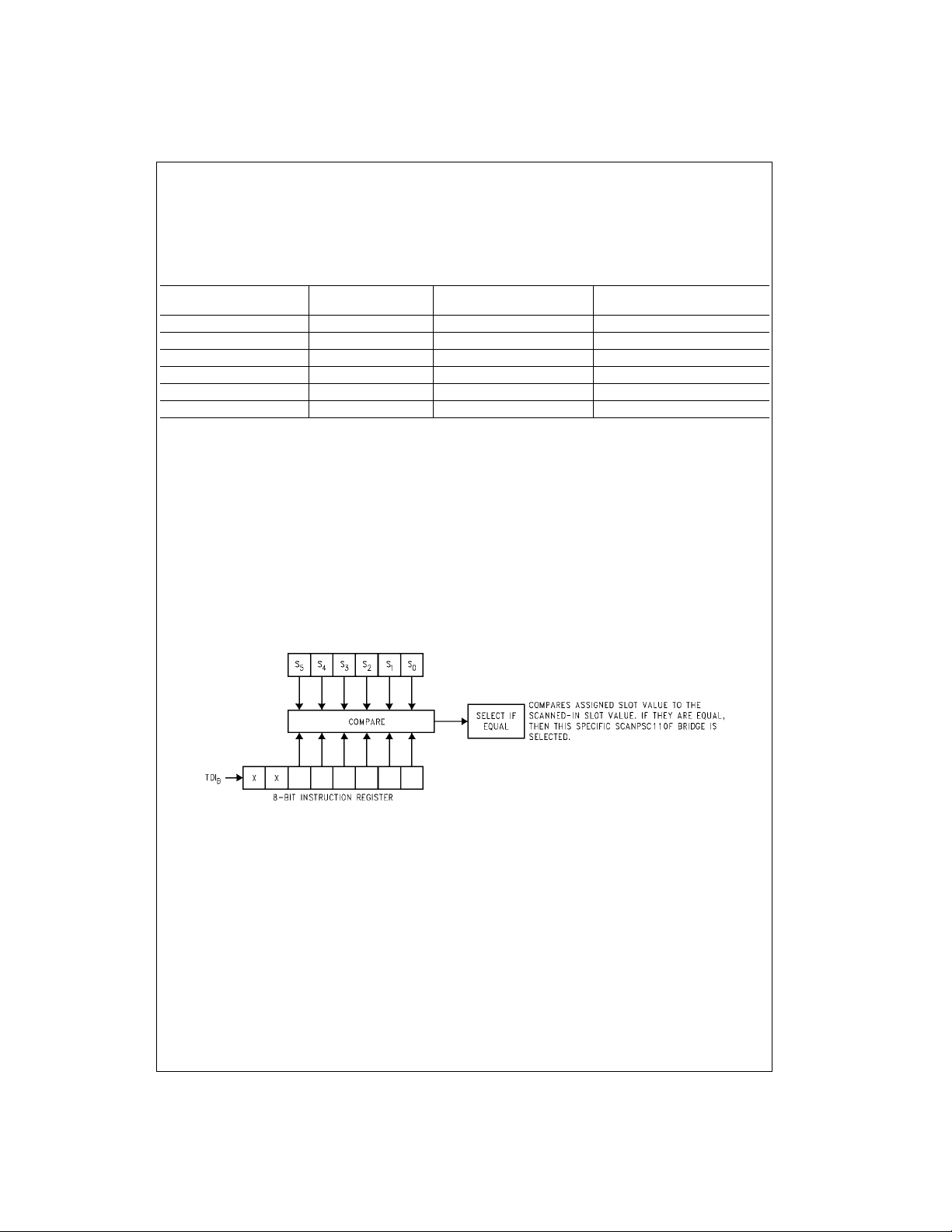
instruction register is compared with the add ress present
on the S
inputs in the Update-IR state. If the six (6)
(0–5)
Addressing. More than one SC ANPS C110F device can be
selected via the Broadcast and Multi-Cast Addressing
modes.
Binary Address
(Note 3)
inputs. The two (2) MSB's are “don't cares”.
TDO
LSBs of the instruction r egister match the address o n the
inputs, (see Figure 6) the SCANPSC110F becomes
S
(0–5)
selected, and is ready to recei ve Level 2 Pro tocol (i.e., further instructions). When the SCANPSC110F is selected, its
device identification register is inserted into the active scan
chain.
All SCANPSC110Fs whose S
address does not match
(0–5)
the instruction register address become unselected . They
will remain unselected until either their TAP Controller
enters the Test-Logic-Reset state, or thei r inst ruct i on r egister is updated with the GOTOWAIT instruction.
State
B
SCANPSC110F
FIGURE 6. Direct Addressing: Device Address Loaded into Instruction Register
BROADCAST ADDRESSING
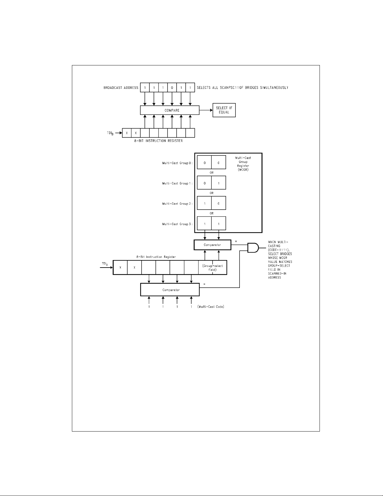
The Broadcast Address a llows a tester to simultaneously
select all SCANPSC110Fs in a test network. This mode is
useful in testing systems which contain multip le identical
boards. To avoid bus contention betwee n sc an- pat h o utp ut
drivers on different boards, each SCANPSC110F’s TDO
buffer is always 3-stated while in Broadcast mode. In this
configuration, the on-c hip Linear Feedback Shift R egister
(LFSR) can be used to ac cumulate a test resu lt signature
for each board that can be read back later by directaddressing each board’s SCANPSC110F.
MULTI-CAST ADDRESSING
As a way to make the broad cast mechanism more selective, the SCANPSC110F provides a “Multi-cast” addressing
mode. A SCANPSC110F's multi-cast group register
(MCGR) can be programmed to assign that
SCANPSC110F to one of four (4) Multi-Cast group s. When
B
SCANPSC110Fs in the W ait-For-Address state are
updated with a Multi-Cast address, all SCANPSC110Fs
whose MCGR matches the Multi-Cast group will become
selected. As in Broadcast m ode, TDO
while in Multi-cast mode.
is always 3-stated
B
9 www.fairchildsemi.com
Page 10
Level 1 Protocol (Continued)
SCANPSC110F
FIGURE 7. Broadcast Addressing: Address Loaded into Instruction Register
FIGURE 8. Multi-Cast Addressing: Address Loaded into Instruction Register
Level 2 Protocol
Once the SCANPSC110F Bridge has been successfully
addressed and selected, its internal registers may be
accessed via Level-2 P rotocol. Leve l-2 Protocol is compliant to IEEE Std. 1149.1 TAP protocol with one exception: if
the SCANPSC110F is selected via the Broadcast or Mu ltiCast address, TDO
buffer must be impl emented this way t o prevent bus contention.)
Upon being sele cted, (i.e., the SCANPSC110F Selection
controller transitions from the Wait-For-Address state to
one of the Selected states), each of the local scan ports
(LSP
, LSP2, LSP3) remains parked in one of the following
1
four TAP Controller states: Test-Logic-Reset, Run-Test/
Idle, Pause-DR, or Pause-IR and the active scan chain will
consist of: TDI
IDCODE register) and out through TDO
→Instruction Register→TDO
TDI
B
www.fairchildsemi.com 10
will always be 3-STATED. (The TDO
B
through the instruction register (or the
B
.
B
B
B
The UNPARK instruction (described later) is used to insert
one or more local scan ports int o the active scan chain.
Tab le 4 describes which local ports are inserted into the
chain, and in what order.
LEVEL 2 INSTRUCTION TYPES
There are two types of instructions (reference Table 5):
1. Instructions that insert a SCANPSC110F register into
the active scan cha in so that th e register can be captured or updated (BYPASS, SAMPLE/PRELOAD,
EXTEST, IDCODE, MODESEL, MCGRSEL, LFSRSEL, CNTRSEL).
2. Instructions that configure local ports or control the
operation of the linear feedback shift register and
counter registers (UNPARK, PARKTRL, PARKRTI,
PARKPAUSE, GOTOWAIT, SOFTRESET, LFSRON,
LFSROFF, CNTRON, CNTROFF). The se instructions,
Page 11
Level 2 Protocol (Continued)
along with any other yet undefined Op-Codes, will
cause the device identifi cation register to be inserted
into the active scan chain.
LEVEL 2 INSTRUCTION DESCRIPTIONS
BYPASS: The BYPASS instructio n sele cts the bypa ss reg-
ister for insertion into the active scan chain when the
SCANPSC110F is selected.
EXTEST: The EXTEST instruction selects the boundary-
scan register for insertion into th e active scan chain. The
boundary-scan register consists of seven “sample only”
shift cells connected t o the S
and OE inputs. On the
(0–5)
SCANPSC110F, the EXTEST instruction performs the
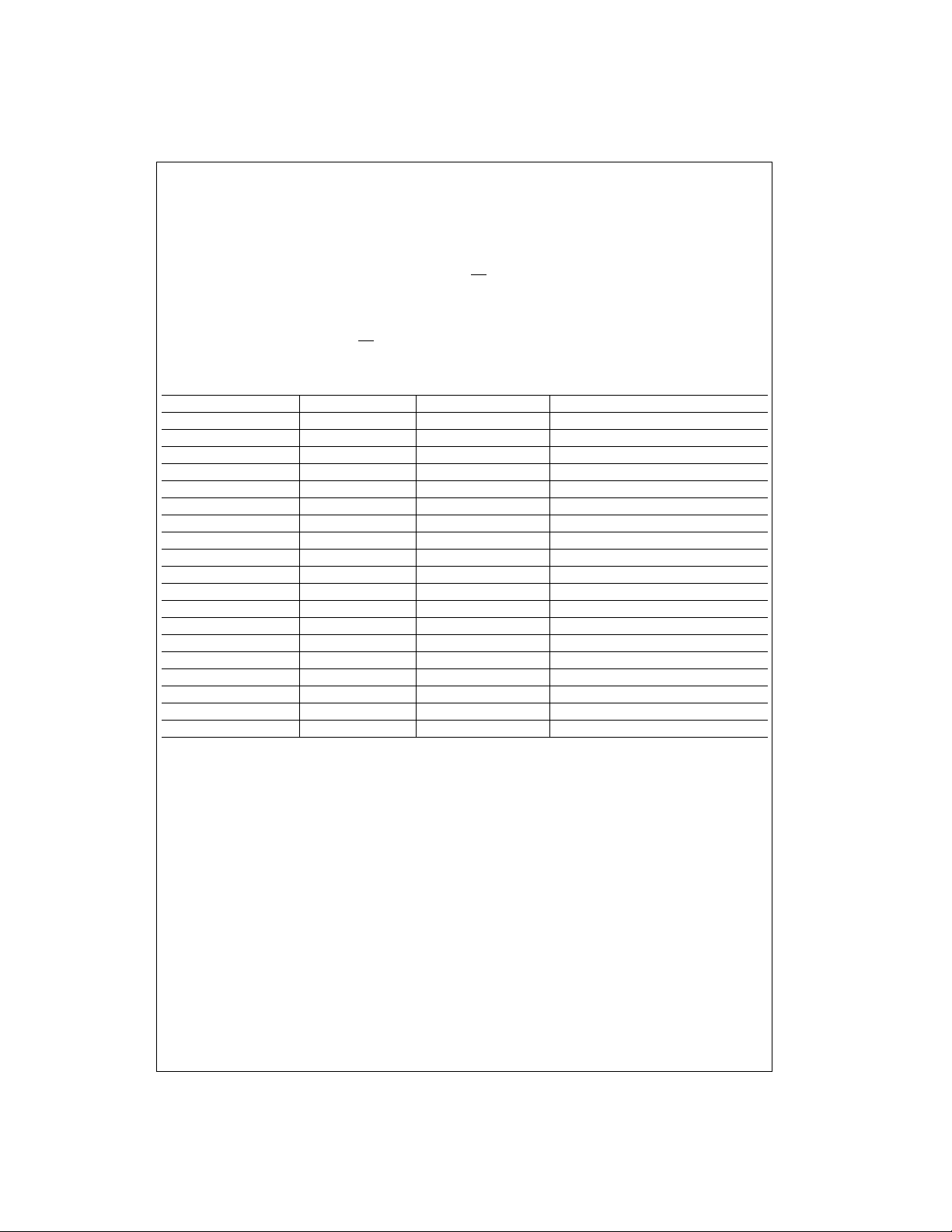
TABLE 5. Level 2 Protocol and Op-Codes
Instructions Hex Op-Code Binary Op-Code Data Register
BYPASS FF 11111111 Bypass Register
EXTEST 00 00000000 Boundary-Scan Register
SAMPLE/PRELOAD 81 10000001 Boundary-Scan Register
IDCODE AA 10101010 Device Identification Register
UNPARK E7 11100111 Device Identification Register
PARKTLR C5 11000101 Device Identification Register
PARKRTI 84 10000100 Device Identification Register
PARKPAUSE C6 11000110 Device Identification Register
GOTOWAIT* C3 11000011 Device Identification Register
MODESEL 8E 1000111 0 Mode Register
MCGRSEL 03 00000011 Multi-Cast Group Register
SOFTRESET 88 10001000 Device Identification Register
LFSRSEL C9 11001001 Linear Feedback Shift Register
LFSRON 0C 00001100 Device Identification Register
LFSROFF 8D 10001101 Device Identification Register
CNTRSEL CE 11001110 32-Bit TCK Counter Register
CNTRON 0F 00001111 Device Identification Register
CNTROFF 90 10010000 Device Identification Register
Other Undefined TBD TBD Device Identification Register
Note 4: All other instructions act on selected SCANPSC110Fs only.
UNPARK: This instruction unparks the Local Scan Port
Network and inserts it into the active scan chai n as conf igured by the Mode register (see Table 4). Unparked L SPs
are sequenced synchronously with the SCANPSC110F's
TA P controller.
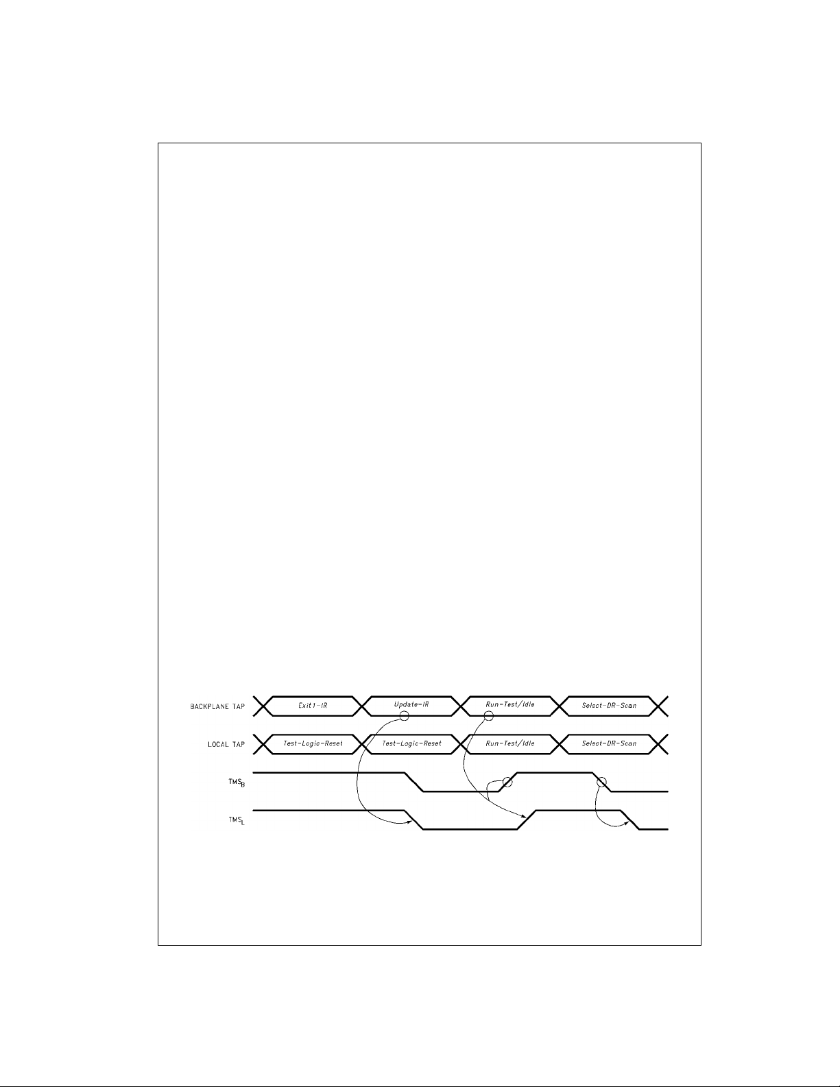
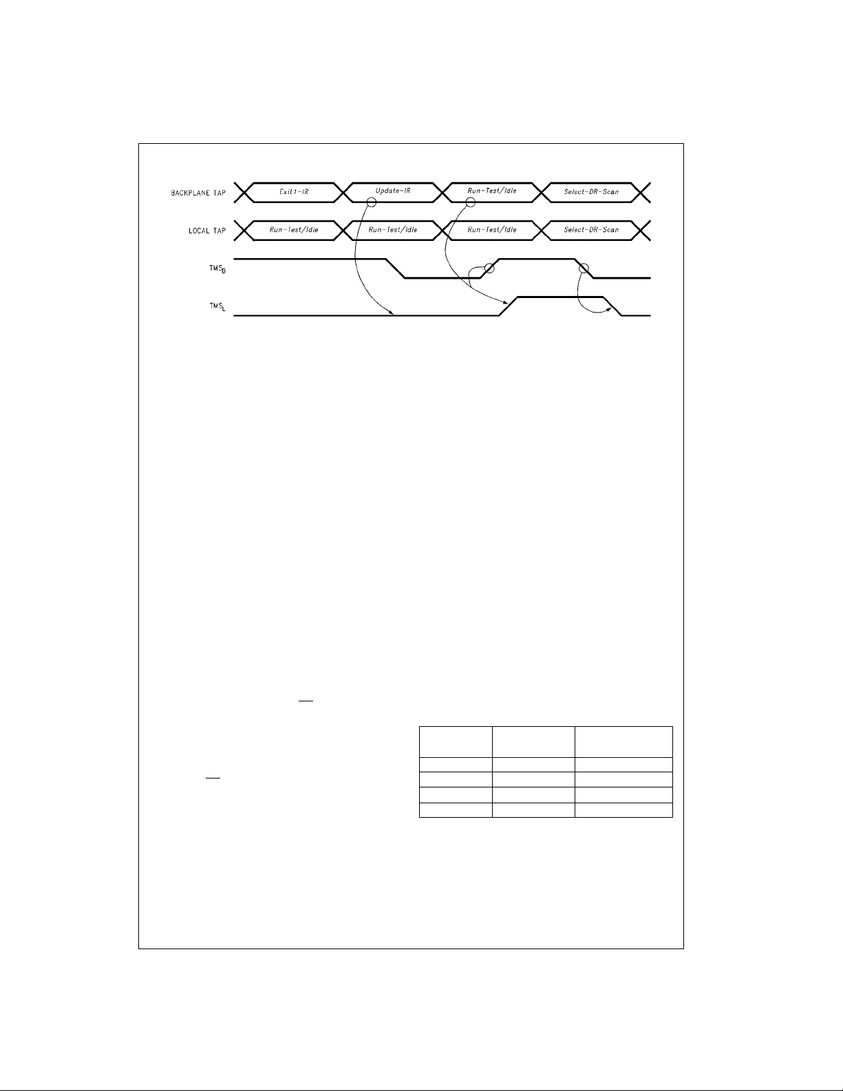
When a LSP has been parked i n the Test-Logic-Reset or
Run-Test/Idle state, it will not become unparked until the
SCANPSC110F's TAP Controller enters the Run-Test/Idle
state following the UNPARK instruction. If an LSP has been
parked in one of the stable pause states (Pause-DR or
Pause-IR), it will not become unparked until the
SCANPSC110F's TAP Controller enters the respective
pause state. (See Figures 9, 10, 11, 12).
PARKTLR: Thi s instruction causes all unparked LSPs to
be parked in the Test-Logic-Reset TAP controller state and
removes the LSP network from the active scan cha in. The
LSP controllers keep the LSPs parked in the Test-Logic-
Reset state by forcin g thei r respect ive TMS
output with a
L
constant logic “1” while the LSP controller is in the Parked-
TLR state (see Figure 4).
PARKRTI: This instruction causes al l unpa rke d LSPs to be
parked in the Run-Test/Idle state. When a LSP
is active
n
same function as the SAMPLE/PRELOAD instruction,
since there aren’t any scannable outputs on the device.
SAMPLE/PRELOAD: The SAMPLE/PRELOAD instruc-
tion selects the boundary-scan register for insertion into the
active scan chain. The b oundary-scan reg ister consists of
seven “sample only” shift c ells connected to the S
OE
inputs.
IDCODE: The IDCODE instructio n sele cts the de vice id en-
tification register for insertion into the active scan chain.
When IDCODE is the current a ctive instruction the device
identification “0FC0E01F” Hex is captured u pon ex i ting the
Capture-DR state.
(unparked), its T MS
signals follow TMSB and the LSP
L
controller state transitions are synchronized with the TAP
Controller state transitions of the SCANPSC110F. When
the instruction register is updated with the PARKRTI
instruction, TMS
will be forced to a constant logic “0”,
L
causing the unparked local TAP Controllers to be parked in
the Run-Test/Idle state. When an LSP
is parked, it is
n
removed from the active scan chain.
PARKPAUSE: The PARKPAUSE instruction has dual func-
tionality. It can be used to park unparked LSPs or to unpark
parked LSPs. The instruction places all unparked LSPs in
one of the TAP Controller pause states. A local port does
not become parked until the SCANPSC110F's TAP Controller is sequenced throu gh Exit1-DR/IR into the Update-
DR/IR state. When the SCANPSC110F TAP Controller is in
the Exit1-DR or Exit1-IR state and TMS
is HIGH, the LSP
B
controller forces a constant logic '0” onto TMS
parking the port in the Pause-DR or Pause-IR state respec-
tively (see Figure 4 ). Another instruction can then be
loaded to reconfigure the local ports or to deselect the
SCANPSC110 F (i.e., MODESEL, GOTOWAIT, etc.).
(0–5)
thereby
L
SCANPSC110F
and
n
11 www.fairchildsemi.com
Page 12
Level 2 Protocol (Continued)
If the PARKPAUSE instruction is given to a bridge whose
LSPs are parked in Pause-IR or Pause-DR, the parked
LSPs will become unparked when the SCANPSC110F’s
TAP controller is sequenced into the respective Pause
state.
The PARKPAUSE instruction was implemented with this
dual functionality to ena ble b ackp l ane te sti ng (inte rco nne ct
SCANPSC110F
testing between boards) with simultaneous Updates and
Captures.
Simultaneous Update an d Capture of several boards can
be performed by parking LSPs of the different boards in the
Pause-DR TAP controller state, after shifting the data to be
updated into the b oundary reg isters of the componen ts on
each board. The bro adcast address is used to select all
SCANPSC110Fs connected to the backplane. The PARK-
PAUSE instruction is scanned into the selected
SCANPSC110Fs and the SCANPSC110F TAP controllers
are sequenced to the Pause-DR state wher e the LSPs of
all SCANPSC110Fs become unparked. The local TAP controllers are then sequenced through the Update-DR,
Select-DR, Capture-DR, Exit1-DR, and parked in the
Pause-DR state, as the SCANPSC110F TAP controller is
sequenced into the Update-DR state. When a LSP is
parked, it is removed from the active scan chain.
GOTOWAIT: This instruction is used to return all
SCANPSC110Fs to the Wait-For-Address state. All
unparked LSPs will be parked in the Test-Logic-Reset TAP
controller state (see Figure 5).
MODESEL: The MODESEL instruction inserts the mode
register into the active scan chain. The mode register
determines the LSPN config uration . Bit 7 of the mode register is a read-only counter status flag.
MCGRSEL: This instruction inserts the multi-cast group
register (MCGR) in to the active scan c hain. The M CGR is
used to group SCANPSC110Fs into multi-cast groups for
parallel TAP sequencing (i.e., to simultaneously perform
identical scan operations).
SOFTRESET: This instruction causes all 3 Port configuration controllers (F igure 4) to enter the Parked-TLR state,
which forces TMS
Test-Logic-Reset state within 5 TCK
HIGH; this parks each local port in the
Ln
cycles.
B
LFSRSEL: This instruction inserts the linear feedback shift
register (LFSR) into the active scan chain, allowing a compacted signature to be shifted ou t of the LFS R during the
Shift-DR state. (The signature is assumed to have been
computed during earlier LFSRON shift operations.) This
instruction disables the L FSR register’s feedback circuitry,
turning the LFSR into a stan dard 16-bit shift reg ister. This
allows a signature to be shifted out of the register, or a
seed value to be shifted into it.
LFSRON: Once this instruction is executed, the linear
feedback shift register samples d ata from the active scan
path (including all unparked TDI
) during the Shift-DR
Ln
state. Data from the scan path is shifted into the linear
feedback shift register an d co mp acte d. Thi s all ows a serial
stream of data to be compressed into a 16-bit signature
that can subsequent ly be shifted out using t he LFSRSEL
instruction. The linear f eedback shift register is no t placed
in the scan chain during this mode. Inst ead, the register
samples the active scan-chain data as it flows from the
LSPN to TDO
.
B
LFSROFF: This instruction terminates linear feedback shift
register sampling. The L FSR retains its curren t state after
receiving this instruction.
CNTRSEL: This instruction inse rts the 32-bit TCK counter
shift register into the active scan chain. This allows the
user to program the numb er of “n” TCK cycles to send to
the parked local ports once the CNTRON instruction is
issued (e.g., for BIST operations). Note that to ensure completion of count-down, the SCANPSC110F should receive
at least “n” TCK
pulses.
B
CNTRON: This instru ction enables the TCK counter. The
counter begins counting down on the first rising edge of
TCK
following the Update-IRTAP controller state and is
B
decremented on each rising edge of TCK
thereafter.
B
When the TCK counter reaches terminal count, “00000000”
Hex, TCK
of all parked LSP's is held LOW. The
L
CNTROFF instru ction must be issued before unparking the LSPs of a SCANPSC110F whose counter has
reached terminal count. This function over-rides the
mode register TCK control bit (bit-3).
CNTROFF: This instruction disables the TCK counter, and
TCK
control is returned to the mode register (bit-3).
L
FIGURE 9. Local Scan Port Synchronization from Parked-TLR Instruction
www.fairchildsemi.com 12
Page 13
Level 2 Protocol (Continued)
FIGURE 10. Local Scan Port Synchronization from Parked-RTI State
Register Descriptions
Instruction Register
The instruction shift register is an 8-bit register tha t is in
series with the scan chain wheneve r the TAP Controller of
the SCANPSC110F Bridge is in the Shift-IR state. Upon
exiting the Capture-IR state, the value “XXXXXX01” is captured into the instruction regi ster, where “XXXXXX” represents the value on the S
When the SCANPSC110F controller is in the Wait-For-
Address state, the instruction register is used for
SCANPSC110F selection via address matching. In
addressing individual SCANPSC110Fs, the chip’s addressing logic performs a comparison betw een a statically-co nfigured (hard-wired) value on that SCANPSC110F’s slot
inputs, and an address which is scanned into the chip’s
instruction register. Binary address codes “000000”
through “111010” (“00” through “3A” Hex) are reserved f or
addressing individua l SCANPSC110Fs. Address “3B” Hex
is for Broadcast mode.
In doing multi-cast (group) addressing, a scanned-in
address is compared against the (previously scanned-in)
contents of a SCANP SC110F's Multi-Cast Group register.
Binary address codes “111110” through “111111” (“3A”
through “3F” Hex) are reserved fo r multi-cast addressing,
and should not be assign ed as SCANPSC110F slot-input
values.
Boundary-Scan Register
The boundary-scan register is a “sample only” shift register
containing cells from the S
allows testing of circui try ext ernal to the SC ANPSC 110F. It
permits the signals flowing between the syste m pins t o be
sampled and examined witho ut interfering with the oper ation of the on-chip system logic.
The scan chain is arranged as follows:
TDI
→OE →S5→S4→
B
S3 →S
2→S1→S0
Bypass Register
The bypass register is a 1-bit register that operates as
specified in IEEE Std. 1149.1 once the SCANPSC110F has
been selected. The register provides a minimum length
serial path for the movem ent of test data between TDI
and the LSPN. This path can be selected when no other
test data register need s to be accessed during a boardlevel test operation. Use of the bypass register shortens
the serial access-path to test data registers located in other
components on a board-level test data path.
inputs.
(0–5)
and OE inputs. The register
(0–5)
→LSPN→TDO
B
Multi-Cast Group Register
“Multi-cast” is a method of simultaneous ly communicating
with more than one selected SCANPSC110F.
The multi-cast group register (MCGR) is a 2-bit register
used to determine which multi-cast group a particular
SCANPSC110F is assigned to. Four addresses are
reserved for multi-cast addressing. When a
SCANPSC110F is in the Wait-For-Address state and
receives a multi-ca st a dd ress , an d if that SCANPSC110F's
MCGR contains a matching value for that multi-cast
address, the SCANPSC110F becomes selected and is
ready to receive Level 2 Protocol (i.e., further instructions).
The MCGR is initialized to “00” upon entering the Test-
Logic-Reset state.
The following actions are used to perform multi-cast
addressing:
1. Assign all target SCANP SC110Fs to a multi-cast gr oup
by writing each individual target SCANPSC110F's
MCGR with the same multi- cast gro up co de ( see Table
6). This configuration step must be done by individually
addressing each target SCANPSC110F, using that
chip's assigned slot value.
2. Scan out the multi-cast group address through the
TDI
input of all SCANPSC110Fs. Note that this occurs
B
in parallel, resulting in the selection of only those
SCANPSC110Fs whose MCGR was previously programmed with the matching multi-cast group code.
TABLE 6. Multi-Cast Group Register Addressing
MCGR Hex Address Binary Address
Bits 1, 0
00 3C XX111100
01 3D XX111101
10 3E XX111110
11 3F XX111111
B
SCANPSC110F
13 www.fairchildsemi.com
Page 14
Register Descriptions (Continued)
TABLE 7. Mode Register Co ntrol of LSPN
Mode Register Scan Chain Configuration (If unparked)
XXX0X000 TDI
XXX0X001 TDI
SCANPSC110F
XXX0X010 TDI
XXX0X011 TDI
XXX0X100 TDI
XXX0X101 TDI
XXX0X110 TDI
XXX0X111 TDI
XXX1XXXX TDI
X = don’t care
Register = SCANPSC110F instruction register or any of the SCANPSC110F test data registers
PAD = insertion of a 1-bit register for synchronization
→Register→TDO
B
→Register→LSP1→PAD→TDO
B
→Register→LSP2→PAD→TDO
B
→Register→LSP1→PAD→LSP2→PAD→TDO
B
→Register→LSP3→PAD→TDO
B
→Register→LSP1→PAD→LSP3→PAD→TDO
B
→Register→LSP2→PAD→LSP3→PAD→TDO
B
→Register→LSP1→PAD→LSP2→PAD→LSP3→PAD→TDO
B
→Register→TDO
B
B
(Loopback)
B
B
B
B
B
B
B
B
Mode Register
The mode regis te r is an 8- bit da t a r egi s ter us e d pr im ar i ly to
configure the Local Sca n Port Network. The mode registe r
is initialized to “00000001” binary upon en tering the Test-
Logic-Reset state.
Bits 0, 1, 2, an d 4 a re use d f or scan chain configu rat io n as
described in Table 7. When the UNPARK instruction is executed, the scan chain configuration will be as shown in
Table 7 above. When all LSPs are parked, the sca n chain
configuration will be
TDI
→SCANPSC110Fregister→TDO
B
TCK
configuration, see Table 8.
Ln
. Bit 3 is used for
B
TABLE 8. Test Clock Configuration
Bit 3 LSP
n
TCK
Ln
1 Parked Stop
0 Parked Run
1 Unparked Run
0 Unparked Run
Bit 3 is normally set to logic “0” so that TCK
is free-running
L
when the local scan ports are parked. When the local ports
are parked, bit 3 can be pro gra mm ed with logic “1”, forcing
all of the LSP TCK
's to stop. This featur e can be used in
L
power sensitive applications to reduce the power consumed by the test circuitry in parts o f the system that ar e
not under test. Bit 3 of the mode register must b e reset
to logic “0” before the UNPARK instruction is executed.
Bit 7 is a status bit for the TCK counter. When the counter
is on and has reached terminal count (Zero) Bit 7 of the
mode register will be high (logic “1”). Bit 7 is read-only and
will be LOW in all other conditions.
Bits 5 and 6 are reserved for future use.
Device Identification Register
The device identification register (IDREG) is a 3 2-bit register compliant with IEEE Std. 1149.1. When the IDCODE
instruction is active, the identification register is loaded with
the value “0FC0E01F” Hex upon leaving the Capture-DR
state (on the rising edge of the TCK
).
B
TABLE 9. Detailed Device Identification (Binary)
Bits Bits Bits Bit
31–28 27–12 11–1 0
Version Part Number Manufacturer 1
Identity
0000 1111 1100 0000 1110 0000 0001 111 1
Linear Feedback Shift Register
The SCANPSC110F contains a “signature compactor”
which supports test result ev aluation in a mult i-chain environment. The signat ure compactor consists of a 1 6-bit linear-feedback shift register (LFSR) which can monitor localport scan data as it is shifted “upstream” from the
SCANPSC110F's local-port network. Once the LFSR is
enabled, the LFSR's state ch anges in a reproducib le way
as each local-port data bit is shifted in from the local-port
network. When all local-port data has been scanned in, the
LFSR contains a 16-bit signatur e value which can be compared against a signature computed for the expected
results vector.
The LFSR uses the following feedback polynomial:
16
F (x)
= X
+ X12 + X3 + X + 1
This signature compac tor is used to compress seria l data
shifted in from the local scan chai n, into a 16- bit signatu re.
This signature can then b e shifted o ut for comp arison with
an expected value. This allows users to test long scan
chains in parallel, via Broadcast or Multi- Cast addressing
modes, and check only the 16-bit signatures from each
module.
The LFSR is initialized with a value of “0000” Hex upon
reset.
32-Bit TCK Counter Register:
The 32-bit TCK counter reg ister enables BIST testin g that
requires “n” TCK cycles, to be run on a parked LS P while
another SCANPSC110F port is bein g tested. The CNTR-
SEL instruction can be used to loa d a count-down value
into the counter registe r via the active scan chain. When
the counter is enabl ed (via the CNTRON instruction), and
the LSP is parked, the local TCKs will stop and be held
LOW when terminal count is reached.
The TCK counter is initialized with a value of “00000000”
Hex upon reset.
www.fairchildsemi.com 14
Page 15
Special Features
SCANPSC110F
BIST SUPPORT
The sequence of instructions to run BIST testing on a
parked SCAN PSC110F Bridge port is as follows:
1. Pre-load the Boundary register of the device under test
if needed.
2. Initialize the TCK counter to 000 00000 He x. Note that
the TCK counter is initialized to 00000000 Hex upon
Test-Logic-Reset, so this step may not be necessary.
3. Issue the CNTRON instruction to the SCANPSC110F,
to enable the TCK counter.
4. Shift the PARKRTI instruction into the SCANPSC110F
instruction register and BIST instruction into the
instruction register of the device under test.
5. Issue the CNTRSEL instruction to the SCANPSC110F.
6. Load the TCK counter (Shift the 32-bit value representing the number of TCK
cycles needed to execute t he
L
BIST operation into the TCK counter register).
7. Bit 7 of the Mode registe r ca n be scan ned to ch eck t he
status of the TCK counter, (MODESEL instr uction followed by a Shift-DR). Bit 7 logic “0” means the counter
has not reached termi nal count, logic “1” means th at
the counter has r eached terminal cou nt and the BIST
operation has completed.
8. Execute the CNTROFF instruction.
9. Unpark the LSP and scan out the result of t he BIST
operation (the CNTROFF instruction mu st be exe c ut ed
before unparking the LSP).
The Self test will begin on the rising edge of TCK
following
B
the Update-DRTAP con troller stat e.
RESET
Reset operations can be performed at three levels. The
highest level resets all SCANPSC110F registers and all of
the local scan chains of selected and unselected
SCANPSC110Fs. This “Level 1” reset is performed whenever the SCANPSC110F TAP Controller enters the Test-
Logic-Reset state. Test-Logic-Reset can be entered sy nchronously by forcing TMS
high for at least five (5) TCK
B
pulses, or asynchron ously by asserting the TRST pin . A
“Level 1” reset forces all SCANPSC110Fs into the WaitFor-Address state, parks all local sca n chains in the TestLogic-Reset state, and initializes all SCANPSC110F regis-
ters.
TABLE 10. Reset Configurations for Registers
Register Bit Width Initial Hex Value
MCGR 2 0
Instruction 8 AA (IDCODE Instruction)
Mode 8 01
LFSR 16 0000
32-Bit Counter 32 00000000
The SOFTRESET instruction is provided to perform a
“Level 2” reset of all LSP's of selected SCANPSC110Fs.
SOFTRESET forces all TMS
signals HIGH, placing the
L
corresponding local TAP Controllers in the Test-Logic-
Reset state within five (5) TCK
cycles.
B
The third level of reset is th e resetting of individual local
ports. An individual LSP can be reset by parking the port in
the Test-Logic-Reset state via the PARKTLR instruction. To
reset an individual LSP that is parked in one of the other
parked states, the LSP must first be unparked via the
UNPARK instruction.
PORT SYNCHRONIZATION
When a LSP is not being acces sed, it is placed in one of
the four TAP Controller states: Test-Logic-Reset, Run-Test/
Idle, Pause-DR, or Pause-IR. The SCANPSC110F is able
to park a local chain by controlling the local Test Mode
Select outputs (TMS
) (see Figure 4). TM SLn is forced
L(1–3)
high for parking in the Test-Logic-Reset state, and for ced
LOW for parking in Run-Test/Idle, Pause-IR, or Pause-DR
states. Local chain access is achieved by issuing the
UNPARK instruction . The LSPs do not become unparked
until the SCANPSC110F TAP Controller is sequenced
through a specified syn chronizati on state. Syn chronizati on
occurs in the Run-Test/Idle state for LS Ps parked in Test-
Logic-Reset or Run-Test/Idle; and in the Pause-DR or
Pause-IR state for ports p arked in Pause-DR or Pause-IR,
respectively.
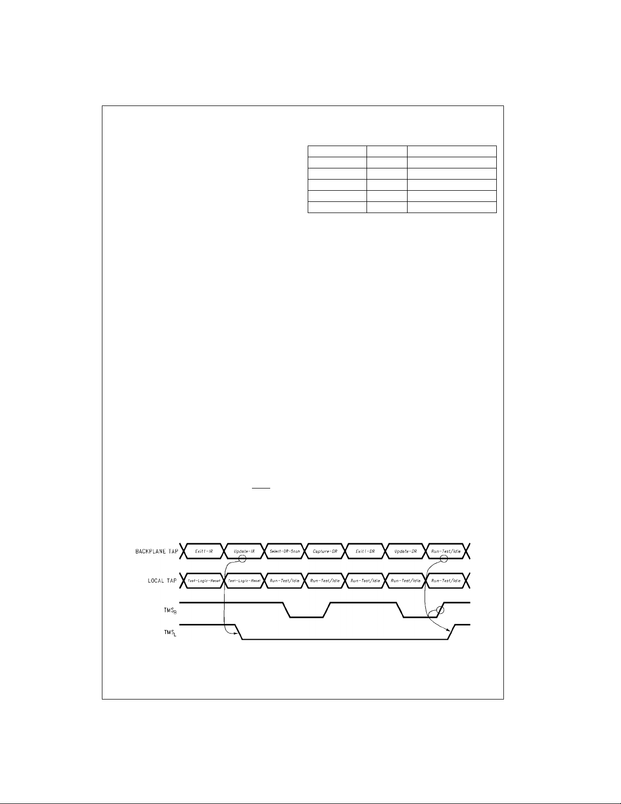
Figures 11, 12 show the waveforms fo r synchronizatio n of
a local chain that was parked in the Test-Logic-Reset state.
B
Once the UNPARK instruction is received in the instruction
register, the LSPC forces TMS
TCK
.
B
LOW on the falling edge of
L
FIGURE 11. Local Scan Port Synchronization on Second Pass
15 www.fairchildsemi.com
Page 16
Special Features (Continued)
This moves the local chain TAP Controllers to the synchronization state (Run-Test/Idle), where they stay until syn-
chronization occurs. If the next state of the SCANPSC110F
TAP Controller is Run-Test/Idle, TMS
TMS
and the local TAP Controllers are synchronized to
B
the SCANPSC110F TAP Controller as shown in Figure 12.
SCANPSC110F
If the next state after Update-IR were Select-DR, TMS
would remain LO W and synchronization would not occur
until the SCANPSC110F TAP Controller entered the Run-
Test/Idle state, as shown in Figure 11.
Each local port has its own Local Scan Port Controller. This
is necessary because th e LSPN can be configured in any
one of eight (8) possible combinations. Either one, some,
or all of the local por ts can be accessed simultaneously.
Configuring the LSPN is a ccomplish ed with t he mode register, in conjunction with the UNPARK instruction.
The LSPN can be unparked in one o f seven d ifferent configurations, as specifie d by bits 0-2 of the mode register.
is connected to
L
Using multiple ports presents not only the task of sy nchronizing the SCANPSC110F TAP Controller with the TAP
Controllers of an individual loca l port, but a lso of synchr onizing the individual local ports to one another.
When multiple local ports are selected for access, it is possible that two ports are parked in different states. This
could occur when p revious operations accessed t he two
L
ports separately and parked them in the two different
states. The LSP Controllers handle this situation gracefully.
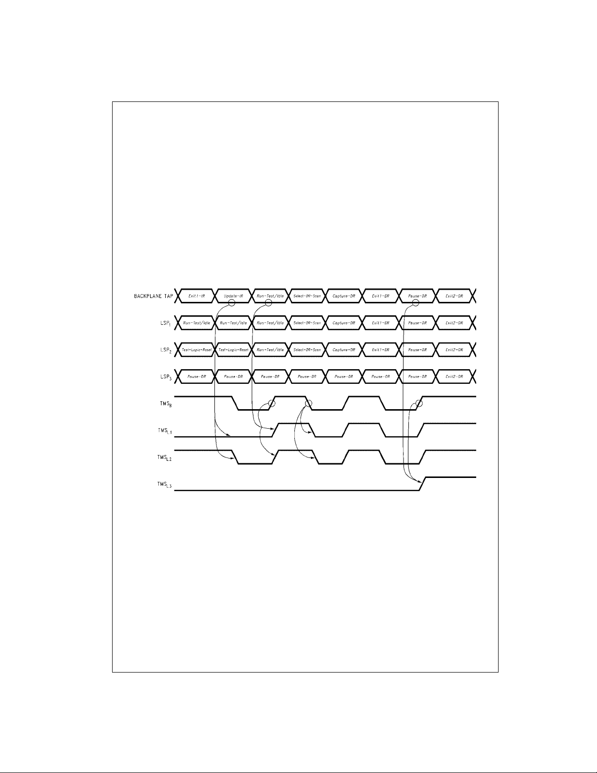
Figure 12 shows th e UNPARK instruction being used to
access LSP
, LSP2, and LSP3 in series (mode reg ister =
1
“XXX0X111” binary). L SP1 and LSP2 become active as the
SCANPSC110F controller is seque nced through the Run-
Test/Idle state. LSP
remains parked in the Pause-DR
3
state until the SCANPSC110F TAP Controller is sequenced
through the Pause-DR sta te. At that point, all three local
ports are synchronized for access via the active scan
chain.
FIGURE 12. Synchronization of the Three Local Scan Ports (LSP
www.fairchildsemi.com 16
, LSP2, and LSP3)
1
Page 17

Absolute Maximum Ratings(Note 5) Recommended Operating
Supply Voltage (VCC) −0.5V to +7.0V
DC Input Diode Current (I
V
= −0.5V −20 mA
I
= VCC +0.5V +20 mA
V
I
DC Input Voltage (V
DC Output Diode Current (I
= −0.5V −20 mA
V
O
V
= VCC +0.5V +20 mA
O
DC Output Voltage (V
DC Output Source/Sink Current (I
DC V
or Ground Current
CC
per Output Pin
DC Latchup Source or Sink Current
Junction Temperature
Storage Temperature
)
IL
) −0.5V to VCC +0.5V
I
)
OK
) −0.5V to VCC +0.5V
O
) ±50 mA
O
±50 mA
±300 mA
+140°C
−65°C to +150°C
ESD Last Pa ssing Voltage (Min) 4000V
Conditions
Supply Voltage (V
Input Voltage (V
Output Voltage (VO)0V to V
Operating Temperature (TA) −40°C to +85°C
Minimum Input Edge Rate
SCAN “F” Series Devices 125 mV/ns
from 0.8V to 2.0V
V
IN
V
@ 4.5V, 5.5V
CC
Note 5: Absolute max imum rating s are those values beyon d w hich damage
to the device may occu r. The databook spe cificatio ns shou ld be met, w ithout exception, to ensure that the system de sign is relia ble over its p ower
supply temperatu re, and ou tput/input loading v ariables. F airchild does not
recommended ope ratio n of SC AN outs ide of reco mme nde d oper atio n conditions.
) 4.5V to 5.5V
CC
)0V to V
I
∆V/∆t
DC Electrical Characteristics
V
TA = 25°CTA = −40°C to +85°C
Symbol Parameter
V
IH
V
IL
V
OH
(TCKLn, TMSLn, TDOLn) Output Voltage 5.5 5.49 5.4 5.4 VIN (TDIB, TMSB, TCKB) = V
V
OH
(TCKLn, TMSLn, TDOLn) Output Voltage 5.5 4.86 4.76 V VIN on S
V
OH
(TDO
) Output Voltage 5.5 4.15 4.15
B
V
OH
(TDOB) Output Voltage 5.5 2.4 2.4 All Outputs Loaded
V
OH
) Output Voltage 5.5 2.4 All Outputs Loaded
(TDO
B
V
OL
(TCKLn,TMSLn, TDOLn) Output Voltage 5.5 0.001 0.1 0.1 VIN (TDIB, TMSB, TCKB) = V
V
OL
(TCKLn,TMSLn, TDOLn) Output Voltage 5.5 0.36 0.44 V VIN on S
V
OL
(TDOB) Output Voltage 5.5 0.1 0.1
V
OL
(TDOB) Output Voltage 5.5 0.55 All Outputs Loaded
V
OL
(TDOB) Output Voltage 5.5 0.55 0.55 All Outputs Loaded
IIN (OE, Maximum Input
TCKB,S
I
IN, MAX
(TRST, TDILn, TDIB, TMSB) Leakage Current
I
IN, MAX
(TRST, TDILn, TDIB, TMSB) Leakage Current
) Leakage Current VIN = GND
(0–5)
Minimum HIGH 4.5 1.5 2.0 2.0
Input Voltage 5.5 1.5 2.0 2.0 VCC −0.1V
Maximum LOW 4.5 1.5 0.8 0.8
Input Voltage 5.5 1.5 0.8 0.8 VCC −0.1V
Minimum HIGH 4.5 4.49 4.4 4.4
Minimum HIGH 4.5 3.86 3.76 I
Minimum HIGH 4.5 3.15 3.15
Minimum HIGH 4.5 2.4 2.4
Minimum HIGH 4.5 2.4
Maximum LOW 4.5 0.001 0.1 0.1
Maximum LOW 4.5 0.36 0.44 I
Maximum LOW 4.5 0.1 0.1
Maximum LOW 4.5 0.55
Maximum LOW 4.5 0.55 0.55
Maximum Input
Maximum Input
CC
(V) Typ Guaranteed Limits
5.5 ±0.1 ±1.0 µA
5.5 2.8 3.6 µAVIN = V
5.5 −385 −385 µAVIN = GND
Units Conditions
V
= 0.1V or
OUT
V
V
= 0.1V or
OUT
V
I
= −50 µA
OUT
V
= −24 mA
OUT
All Outputs Loaded
VI
= −50 µA
OUT
I
= −32 mA
OUT
V
I
= −24 mA
OUT
V
I
= +50 µA
OUT
V
= +24 mA
OUT
All Outputs Loaded
VI
= +50 µA
OUT
I
= +48 mA
OUT
V
I
= +64 mA
OUT
V
VIN = VCC or
CC
(0-5)
(0–5)
and TDl
and TDI
(1–3)
(1–3)
= VIH, V
IH
IL
= VIH, V
SCANPSC110F
CC
CC
IL
IL
17 www.fairchildsemi.com
Page 18
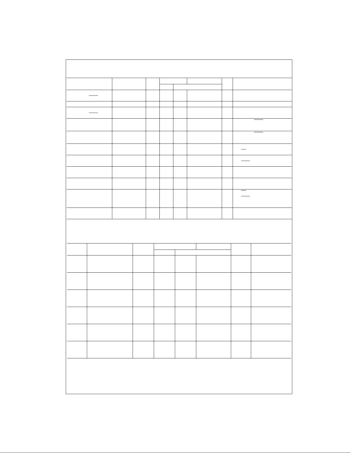
DC Electrical Characteristics (Continued)
V
TA = 25°CTA = −40°C to +85°C
Symbol Parameter
I
IN, MIN
, TMSB, TRST, TDILn) Leakage Current
(TDI
B
SCANPSC110F
I
CCT
I
CCT
, TMSB, TRST, TDIL) Test one at a time with others floating
(TDI
B
I
CC
Minimum Input
Maximum ICC/Input 5.5 0.6 1.5 mA VIN = VCC −2.1V
Maximum ICC/Input
Maximum Quiescent
Supply Current TDI
I
CC, MAX
Maximum Quiescent
Supply Current TDIL = GND
I
OLD
(TCK
, TMSLn, TDOLn) Output Current VIN (OE) = VIL (Note 6)
Ln
I
OLD
Minimum Dynamic
Minimum Dynamic
(TDOB) Output Current VIN (TRST) = VIH (Note 6)
I
OHD
Minimum Dynamic
(TCKLn, TMSLn, TDOLn) Output Current (Note 6)
I
OHD
(TDO
) Output Current (Note 6)
B
I
OZ
Minimum Dynamic
Maximum 3-STATE VIN (OE) = V
Leakage Current 5.5 ±0.5 ±5.0 µAVIN (TRST) = V
I
OS
Output Short
(TDOB) Circuit Current min (Note 7)
Note 6: Maximum test dura tio n of 2 m s . One output loaded at a tim e.
Note 7: Maximum test duration not to exceed 1 second.
CC
(V) Typ Guaranteed Limits
Units Conditions
5.5 −160 −160 µAVIN = GND
5.5 0.6 1.65 mA
5.5 16 88 µA
5.5 2.35 2.4 mA
5.5 75 mA
5.5 94 94 mA
5.5 −75 mA
5.5 −40 −40 mA
VIN = VCC −2.1V
TDIB, TMSB, TRST,
= V
L
TDIB, TMSB, TRST,
V
= 1.65V max
OLD
V
= 0.8V
OLD
V
= 3.85V max
OHD
V
= 2.0V max
OHD
VO = VCC, GND
5.5 −100 −100
mA VO = 0.0V
CC
IH
IL
Noise Specifications
V
Symbol Parameter
V
OLP
Quiet Output Figure 14
CC
(V) Type Guaranteed Limits
Maximum Dynamic 5.0 0.3 0.6 V (Note 8)
V
V
OLV
OL
Quiet Output Figure 14
Minimum Dynamic 5.0 0.3 −0.6 V (Note 8)
V
V
OHP
OL
Quiet Output Figure 14
Maximum Dynamic 5.0 VOH + 0.5 VOH + 1.0 V (Note 9)
V
V
OHV
OH
Quiet Output Figure 14
Minimum Dynamic 5.0 VOH − 0.7 VOH − 1.2 V (Note 9)
V
V
IHD
OH
Minimum HIGH
Dynamic Input 5.5 1.9 2.2 2.2 V (Note 10)
Voltage Level
V
ILD
Maximum LOW
Dynamic Input 5.5 1.4 0.8 0.8 V (Note 10)
Voltage Level
Note 8: Maximum number of outputs that can switch simultaneously is n. (n−1) outputs are swit ch ed LOW and one output held LOW.
Note 9: Maximum number of outputs that can switch simultaneously is n. (n−1) outputs are swit ch ed HIGH and one output held HIGH.
Note 10: Maximum number of data inputs (n) switching. (n−1) input switchin g 0V to 3V. Input under test switching 3V to threshold (V
www.fairchildsemi.com 18
TA = +25°CT
= −40°C to +85°C
A
Units Conditions
).
ILD
Page 19
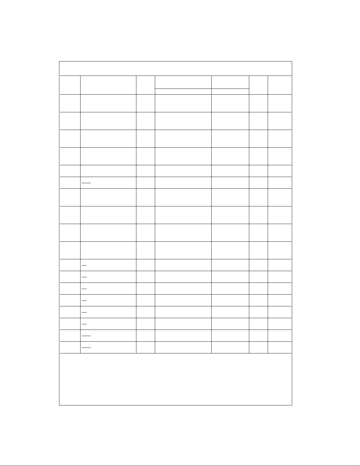
AC Electrical Characteristics
= +25°CT
T
V
Symbol Parameter
t
, Propagation Delay
t
t
t
t
t
t
t
t
t
t
t
t
t
t
t
t
t
t
t
t
t
t
t
t
t
t
t
t
t
t
t
t
t
t
PHL
PLH
PHL
PLH
PHL
PLH
PHL
PLH
PHL
PLH
PLH
PZL
PZH
PLZ
PHZ
PZL
PZH
PLZ
PHZ
PZL
PZH
PLZ
PHZ
PZL
PZH
PLZ
PHZ
PZL
PZH
PLZ
PHZ
PLZ
PHZ
PLZ
PHZ
TCKB↓ to TCK
TCKB↑ to TCK
Ln
Ln
, Propagation Delay
TCKB↓ to TDO
TCKB↓ to TDO
Ln
Ln
, Propagation Delay
TCKB↓ to TMS
TCKB↓ to TMS
Ln
Ln
, Propagation Delay
TCKB↓ to TDO
TCKB↓ to TDO
B
B
, Propagation Delay 5.0 2.5 8.0 12.0 2.5 13.0
TMSB to TMS
Ln
Propagation Delay
TRST
to TMS
Ln
, Enable Time
TCKB↓ to TDO
TCK
↓ to TDO
B
Ln
Ln
, Disable Time
TCKB↓ to TDO
TCK
↓ to TDO
B
Ln
Ln
, Enable Time
TCKB↓ to TDO
TCK
↓ to TDO
B
B
B
, Disable Time
TCKB↓ to TDO
TCK
↓ to TDO
B
B
B
, Enable Time 5.0 3.0 10.0 15.0 3.0 17.5
OE to TDO
Ln
, Disable Time
OE to TDO
Ln
, Enable Time
OE to TMS
Ln
, Disable Time
OE to TMS
Ln
, Enable Time
OE to TCK
Ln
, Disable Time
OE to TCK
Ln
, Disable Time
TRST to TDO
B
, Disable Time
TRST to TDO
Ln
CC
(V)
5.0 3.0 8.5 12.5 3.0 13.5 ns Figure 13
5.0 3.0 10.0 14.0 3.0 15.0 ns Figure 13
5.0 3.5 15.0 23.0 3.5 25.0 ns Figure 13
5.0 3.0 9.5 14.5 3.0 15.5 ns Figure 13
5.0 4.5 19.0 26.5 4.5 28.5 ns Figure 15
5.0 4.0 12.5 18.5 4.0 20.5 ns
5.0 1.5 7.5 12.0 1.5 13.5 ns
5.0 4.0 12.0 17.0 4.0 18.5 ns
5.0 2.0 9.0 13.0 2.0 14.5 ns
5.0
5.0
5.0
5.0
5.0
5.0
5.0
A
C
= 50 pF CL = 50 pF
L
Min Typ Max Min Max
2.5 8.5 12.5 2.5 13.5
3.0 10.0 14.5 3.0 15.5
4.5 14.5 21.5 4.5 23.0
2.5 9.0 13.5 2.5 15.0
1.5 7.5 12.0 1.5 13.0
3.0 11.0 15.5 3.0 17.0
2.0 8.5 14.0 2.0 15.0
2.5 9.0 13.5 2.5 14.5
2.0 9.5 14.0 2.0 15.5
3.0 10.0 14.0 3.0 15.0
1.0 7.0 11.0 1.0 12.0
1.0 8.0 13.0 1.0 13.5
2.0 8.0 11.5 2.0 12.5
1.5 6.5 10.0 1.5 11.0
1.0 5.0 9.0 1.0 10.0
1.0 6.0 10.0 1.0 10.5
2.0 8.0 11.5 2.0 12.5
1.5 6.5 10.0 1.5 11.0
1.0 5.0 9.0 1.0 10.0
1.0 6.0 10.0 1.0 10.5
2.5 11.0 16.5 2.5 18.0
3.0 12.0 16.5 3.0 18.0
2.5 11.5 17.5 2.5 19.0
1.5 11.5 17.5 1.5 19.0
= −40°C to +85°C
A
Units
Figure
Number
ns Figure 13
ns Figure 16
ns Figure 16
ns Figure 16
ns Figure 16
ns Figure 16
ns Figure 16
ns Figure 15
ns Figure 15
SCANPSC110F
19 www.fairchildsemi.com
Page 20
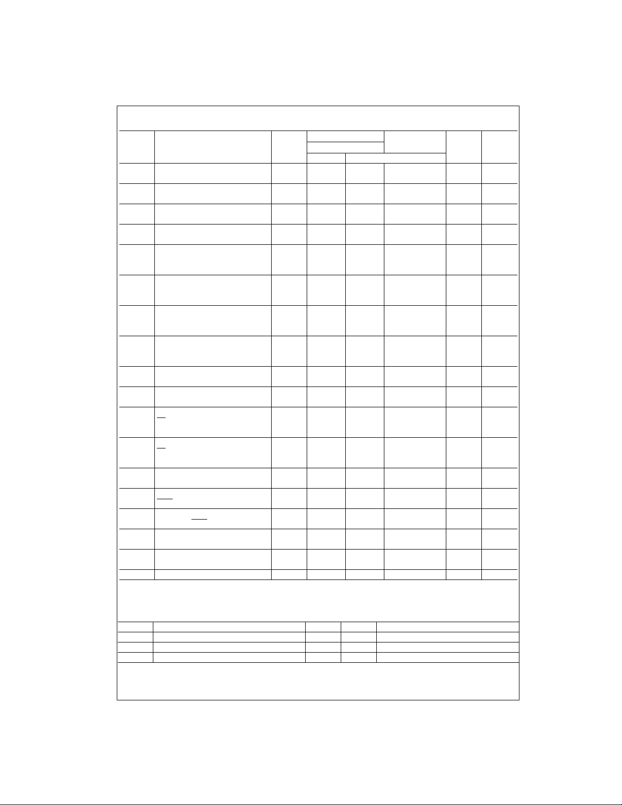
AC Electrical Characteristics
= +25°CT
T
Symbol Parameter
t
S
SCANPSC110F
t
H
t
S
Setup Time
to TCKB↑
TMS
B
Hold Time
TMS
to TCKB↑
B
Setup Time
TDIB to TCKB↑
t
H
t
S
Hold Time
to TCKB↑
TdI
B
Setup Time
S
to TCKB↓ 5.0 7.5 12.5 12.5 ns
n
V
CC
(V)
5.0 3.5 8.0 8.0
5.0 −0.5 4.0 4.0 ns Figure 13
5.0 1.5 6.0 6.0 ns Figure 13
5.0 1.0 4.0 4.0 ns Figure 13
A
C
= 50 pF CL = 50 pF
L
Typ Guaranteed Minimum
(in Update-DR state)
t
H
Hold Time
S
to TCKB↓ 5.0 −3.0 0.0 0.0 ns
n
(in Update-DR state)
t
S
Setup Time
S
to TCKB↑ 5.0 0.0 4.0 4.0 ns
n
(in Capture-DR or Capture-IR state)
t
H
Hold Time
S
to TCKB↑ 5.0 1.5 6.0 6.0 ns
n
(in Capture-DR or Capture-IR state)
t
S
t
H
t
S
Setup Time
TDI
to TCKB↑
Ln
Hold Time
TDILn to TCKB↑
5.0 −1.5 2.0 2.0 ns Figure 13
5.0 2.0 6.0 6.0 ns Figure 13
Setup Time
to TCKB↑ 5.0 0.0 4.0 4.0 ns
OE
(in Capture-DR state)
t
H
Hold Time
to TCKB↑ 5.0 0.0 4.0 4.0 ns
OE
(in Capture-DR State)
t
W
t
WL
t
REC
t
OSHL
t
OSLH
t
OSHL
t
OSLH
f
MAX
Note 11: Skew is defined as the abs olute valu e of th e differenc e betw een the actual p ropag ation de lays for any two separate output s of the same dev ice.
The specification applies to any outputs s w it ch ing HIGH-to-LOW (t
Clock Pulse Width
(H or L)
TCK
B
Clock Pulse Width
TRST
(L)
Recover Time
TCKB↑ from TRST
, Output-to-Output Skew
TCK
Ln
, Output-to-Output Skew
TMSLn (unparked)
5.0 16.0 20.0 24.0 ns Figure 13
5.0 6.0 10.0 10.0 ns Figure 15
5.0 −2.0 2.0 2.0 ns Figure 15
5.0 1.0 1.0 ns (Note 11)
5.0 2.0 2.0 ns (Note 11)
Maximum Clock Frequency 5.0 25 MHz
), or LOW-to-HIGH (t
OSHL
). The specification is guaranteed but not tested.
OSLH
= −40°C to +85°C
A
Units
Figure
Number
Capacitance
Symbol Parameter Typ Units Conditions
C
IN
C
OUT
C
PD
www.fairchildsemi.com 20
Input Pin Capacitance 5.0 pF VCC is Open
Output Pin Capacitance 6.5 pF VCC is Open
Power Dissipation Capacitance 50 pF VCC = 5.0V
Page 21
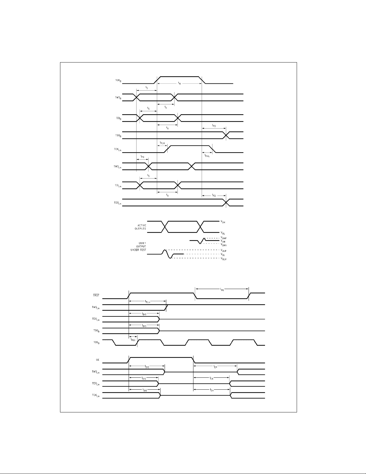
AC Waveforms
FIGURE 13. Waveforms for an Unparked SCANPSC110F Bridge in the SHIFT-DR (IR) TAP Controller State
SCANPSC110F
Note A: V
Note B: Input pulses have the following characteristics: f = 1 MHz, t
OHV
and V
are measured with respect to ground reference.
OLP
FIGURE 14. Quiet Output Noise Voltage Waveform
FIGURE 15. Reset Waveforms
FIGURE 16. Output Enable Waveforms
= 3 ns, tf = 3 ns, skew ≤ 150 ps.
r
21 www.fairchildsemi.com
Page 22
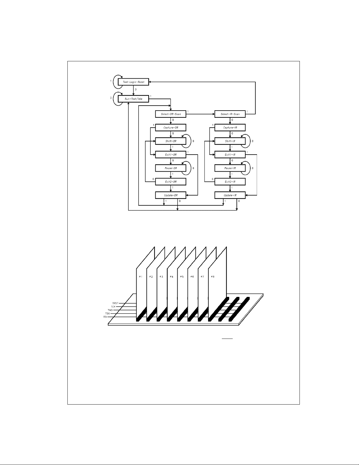
Appendix
SCANPSC110F
Note: The value of the TMS during the rising edge of TCK is located next to ea c h t ransition.
FIGURE 17. IEEE 1149.1 TAP Controller State Diagram
Applications Example
FIGURE 18. Boundary Scan Backplane with 10 Card Slots, 8 Slots Are Filled with Boards
The following sequence gives an example of how one
might use the SC ANPSC110F Bridge to perform 1149.1
operations via a multi- drop scan backplane. The system
involved has 10 card slots, 8 of wh ich are filled with modules, and 2 slots are empty. (See Figure 18).
More Inform ation can be found in Application Notes:
AN-1023 Structural System Test via IEEE Std. 1149.1
with SCANPSC110F Hierarchical and Multidrop Addressable JTAG Port
AN-1022 Boundary Scan, An Ena bling Technolo gy for
System Level Embedded Test
www.fairchildsemi.com 22
1. After the system is powered u p a level-1 reset is performed via the TRST
SCANPSC110F and local) are asynchronou sly forced
into the Test-Logic-Reset state. All LSP Controllers are
in the parked Test-Logic-Reset state; this forces the
TMS
outputs of each port to a logic “1”, keeping all
L
board TAPs in the Test-Logic-Reset state.
2. The first task of the tester is to find out which slots are
occupied on the backplane. T his is accomplished by
performing a serial poll of e ach slot a ddr ess in the system, as assigned by the S
SCANPSC110F in the system.
input. All TAP Controllers (both
value of each
0–5
Page 23

Each target slot address is addressed by first sequencing all SCANPSC110Fs on the backplane to the Shift-
IR state, and then by shiftin g in the addr ess of the ta rget slot. The SCANPSC110F TAP controller is then
sequenced through the Update-IR state. If a
SCANPSC110F with the matching slot identification is
present, it is selected. Al l other SCANPSC110Fs are
unselected. To determine whether that slot contain s a
selected SCANPSC110F, the tester must read back the
SCANPSC110Fs S
value (if present).
0–5
The tester moves the selected SCANPSC110F from
the Update-IR st ate back to the Shift-IR state, and the
instruction register is then scanned while loading the
next instruction (GOTOWAIT). During the Capture-IR
state of the TAP Controller, a “01” pattern is loaded into
the two least significant b its of the SCANPSC110F's
instruction register, and the most significant six bits
capture the value on the S
pins. The captured data
0–5
is shifted out while the GOTOWAIT command is shifted
in. If an “all ones” pattern is returned, a boa rd do es n ot
exist at that location. (The “all ones” pattern is caused
by the pull-up resistor on the TDI input of the c ontroller,
as required for 1149.1 compliance.)
At the end of instruction register sca n, the GOTOWAIT
command is issued and all SCANPSC110F selection
controllers enter the Wait-For-Address state. This
allows the next SCANPSC110F in the polling sequence
to be addressed. The polling process i s repeated for
every possible board address in the system. In this
example, the tester finds that boards #1 through #8 are
present, and boards #9 and #10 are missing. Therefore, it will report back its findings and will not at tempt
to test the missing boards.
3. Infrastructure testing of the populated boa rds may now
proceed. The tester addr esses the SCANPS C110F on
Board #1 for test operations. SCANPSC110F #1 is now
selected, while all others are unselected.
Board #1 is wired such that all LSP
's are connected to
n
individual scan chains. The fi rst objective is to tes t the
scan chain integrity of the board. For this task, it is
more efficient to configure the LSPN such that all thr ee
chains are placed in series. To accomplish this, the
MODESEL instruction is issued to p lac e the mo de re gister into the active scan cha in, and the binary value
“00000111” is shifted into the mode register. The
UNPARK instruction is then issued to access all three
local chains.
Once the UNPARK instru ction has been updated a nd
the SCANPSC1 10F TAP controller is synchronized with
the local TAP's, the scan chain integrity test can be performed on the lo cal scan chains. This test is done by
performing a Capture-IR and then shifting the scan
chain checking the 2 lea st significant bits of e ach com ponents instruction re giste r f or “01”. If the LSB's of any
component in the scan chain are not “01”, the test fails.
Diagnostic software can be used to narrow down the
cause of the failure. Ne xt the device identification of
each component in the scan cha in is checked. This is
done by issuing the IDCODE inst ruction to each com ponent in the scan chain. Components that do not support IDCODE will insert their bypass register into the
active scan chain.
After the IDCODE register scan, the GOTOWAIT
instruction is issued to reset the local s can ports and
return the SCANPSC110F Selection controller to the
Wait-For-Address state. A sequence similar to step 3 is
repeated for each board in the system.
4. Next, the tester addr esses Board #1 to perform int erconnect testing. For this ta sk, it is e fficient to config ure
the LSPN such that all three chains are placed in
series. Therefore, the Mode register should be programmed with the binary value “00000111” (this was
done in step 3 above an d need not be repeat ed u nless
a Test-Logic-Reset was performed since then). The
UNPARK instruction is issued to access all three local
chains.
Once the UNPARK instruction has been loaded and
the SCANPSC110F is synchronized with the local
TAPs, normal 1149.1 scan operations may com me nce .
To test the interconnect on Board #1, an instruction
register scan sequence is performed and the SAMPLE/
PRELOAD instruction is loaded into the instruction register of all target devices. The BYPASS instruction is
loaded into the instruction register of SCANPSC11 0F
#1. A data register sc an is now performed to preload
the first test vector to be applied to the interconnect.
5. After the preloa d operation is perfo rm ed , a n in stru cti on
register scan is used t o load the EXTEST instruction
into all TAPs (BYPASS loaded into SCANPSC110F
#1). The appropria te sequencing is now perfo rmed to
apply patterns in order to test the interconnect on
Board #1.
6. Upon completion o f the in terconnect test on Board #1 ,
the local chains must be p arked. The PARKTLR com-
mand is loaded into the instruction register, and the
TMS
outputs of the three local chains are forced
Ln
HIGH, sending the three local TAPs into the Test-Logic-
Reset state.
7. Now that the Bo ard #1 interconnect ha s been tested,
the interconnect on the other boards in the system
must be checked. All SCA NPSC110F are returned to
the Wait-For-Address state by issuin g the GOTOWAlT
instruction. Board #2 is addressed next, followed by the
rest of the boards in the system. A seque nce similar to
steps 4 through 6 is used for each board.
8. Assume that boards #6, #7 and #8 are identical, so that
it is possible to test them simultaneously. The tester
first addresses Board #6. Next the MCGRSEL instruction is issued to place the Multi-Cast Group register into
the active scan chain, and the binary value “01” is
shifted into the MCGR. The GOTOWAIT instruction is
then issued returning a ll SCANPSC 110F's to the Wait-
For-Address state. The MCGR for SCANPSC 110F #7
and SCANPSC110F #8 are programm ed the same as
Board #6. Next the Mu lti-Cast address “00111101” is
issued by the tester, which causes the SCANPSC110F
Selection controller of SCANPSC110F #6–#8 to enter
the Selected-Multi-Cast state. The LFSRON instruction
is then issued to enable the signature com paction circuitry on the selected SCANP SC110Fs. The SAMPLE/
PRELOAD and EXTEST instructions are then used to
test the interconnects, simi lar to steps 4 and 5 above.
When the test sequence is comp lete, the GOTOWAIT
instruction is issued returning all SCANPSC110Fs to
the Wait-For-Address state . SCANPSC110Fs #6, #7,
and #8 are then add ressed one at a time to r ead bac k
the test signature from the LFSR (the LFS R is read by
selecting it with the LFSRSEL instruction, then scanning out its contents.
SCANPSC110F
23 www.fairchildsemi.com
Page 24
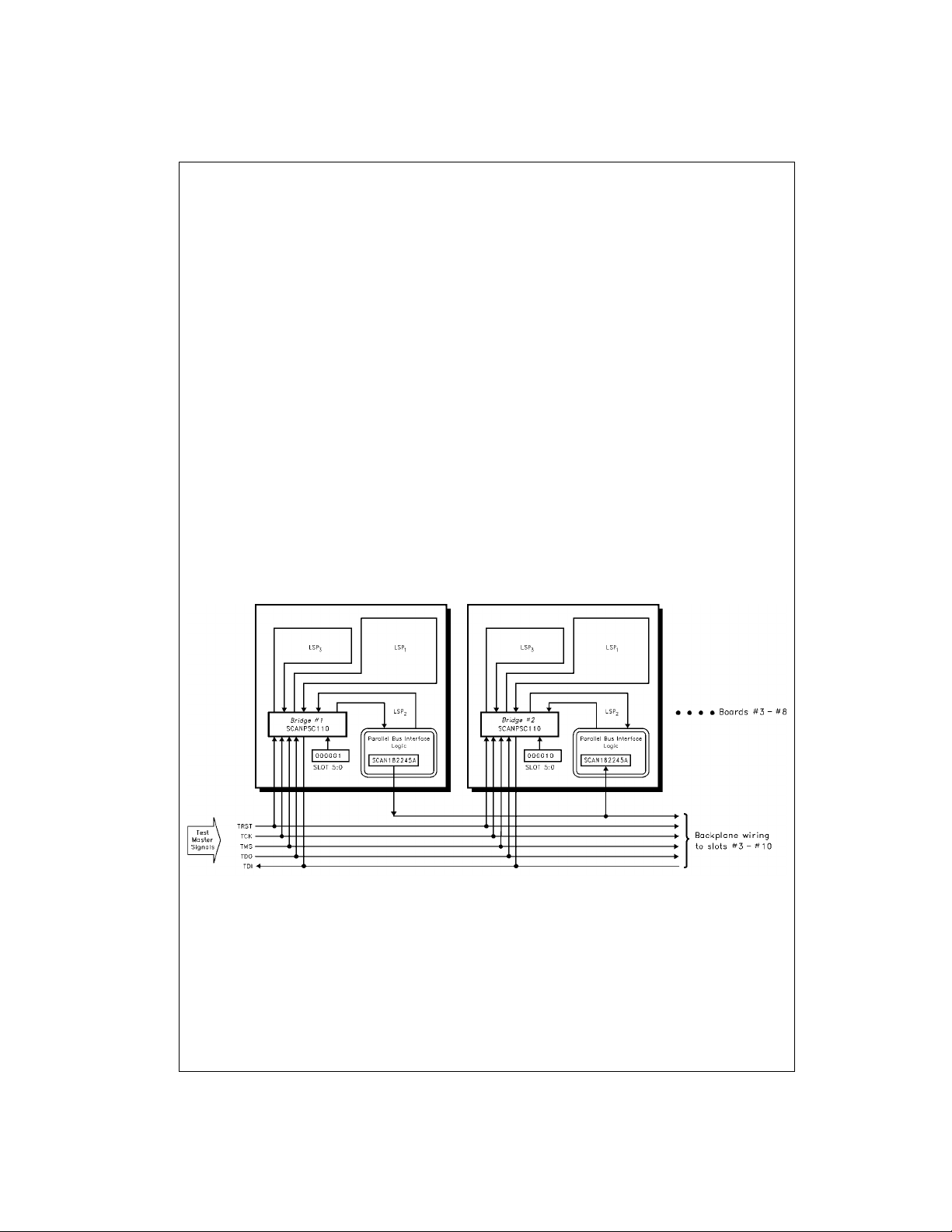
9. After testing t he interconnec t on the indi vidual boards ,
the next step is to test the backplane interconnect. This
is a pair-wise t est between Board #1 and each of the
other boards. Board #1 drives test patterns onto the
backplane wiring, and the currently addressed slave
board senses the w ritten data via its backp lane scan
interface. In this example, the interconnect between
Board #1 and Bo ar d # 2 is teste d first. To test this inter-
SCANPSC110F
connect, the 1149.1-compliant b ackplane tr ansceiver s,
SCAN182245A, SCAN ABT Test Access Logic, on
each board must be accessed for scan operations (see
Figure 19 ). For more informat ion on SCAN ABT live
insertion capabilities, refer to the SCAN182245A
datasheet.
First, the system master ( Board #1) is addressed and
selected. The 1149.1-compl iant SCAN ABT tra nsceivers reside on the chain connected to LS P
2
#1. The mode register is re-configured so that only port
LSP
is in the chain, and the UNPARK instruction is
2
then used to access this chain. The appropriate
instruction register an d data register scan se quencing
is then performed to apply a pattern to the backplane
using the SCAN ABT bus transceiver.
10. To test the ba ckplane interconne ct, LSP
of Board #1
2
must be parked in the Run-Test/Idle TAP controller
state, so that the EXTEST command will stay active
when Board #1 is d e-selected (the PARKRTI instruction is issued). The GOTOWAIT instruction is then
issued to return all boards to the Wait-For-Address
state. Each one of the slave boar ds is th en ad dr esse d,
on Board
one at a time, to sample the backplane signals being
driven by Board #1. For example, Board #2 is
addressed. The mode register is reconfigured, (if
needed), to select the scan cha in (LSP
) that includes
2
the SCAN ABT backpl ane transceivers for Board #2.
The UNPARK instruction is issued to unpark LSP
n
and
insert it into the active scan ch ain. T he SAMPLE/PRE-
LOAD instruction is issued to the SCAN ABT backplane transceivers, (BYPASS to oth er components in
the scan chain). The backplane is sampled by
sequencing the TAP controller through the Capture-DR
state and the data is shifte d out and checked by the
tester. The PARKRTI instruction is then given to park
LSP
of Board #2 in the Run-Test/Idle state, and the
n
GOTOWAIT instruction is issued to return all
SCANPSC110Fs to the Wait-For-Address state so that
the next board, (Board #3), c an be s ampled. This pr ocedure is repeated for boar ds #3–#8, then Board #1 is
selected again, a new p attern is shifte d out and dr iven
by the EXTEST command, and the slave b oards are
again sampled.
11. Step 10 is repeated until the ba ckplane interconnect
has been sufficiently tested.
12. When testing is complete, the c ontroller sends out the
SOFTRESET instruction to all SCANPSC110Fs. This is
accomplished by first using the broadcast address,
“3B” Hex, to select all SCANPSC110Fs. The SOFTRESET comm and is then loaded, causing TMS
L(1–3)
sig-
nals to go HIGH; this drives all local TAPs into the Test-
Logic-Reset state within five TCK cycles.
FIGURE 19. Testing the Backplane Interconnections
www.fairchildsemi.com 24
Page 25
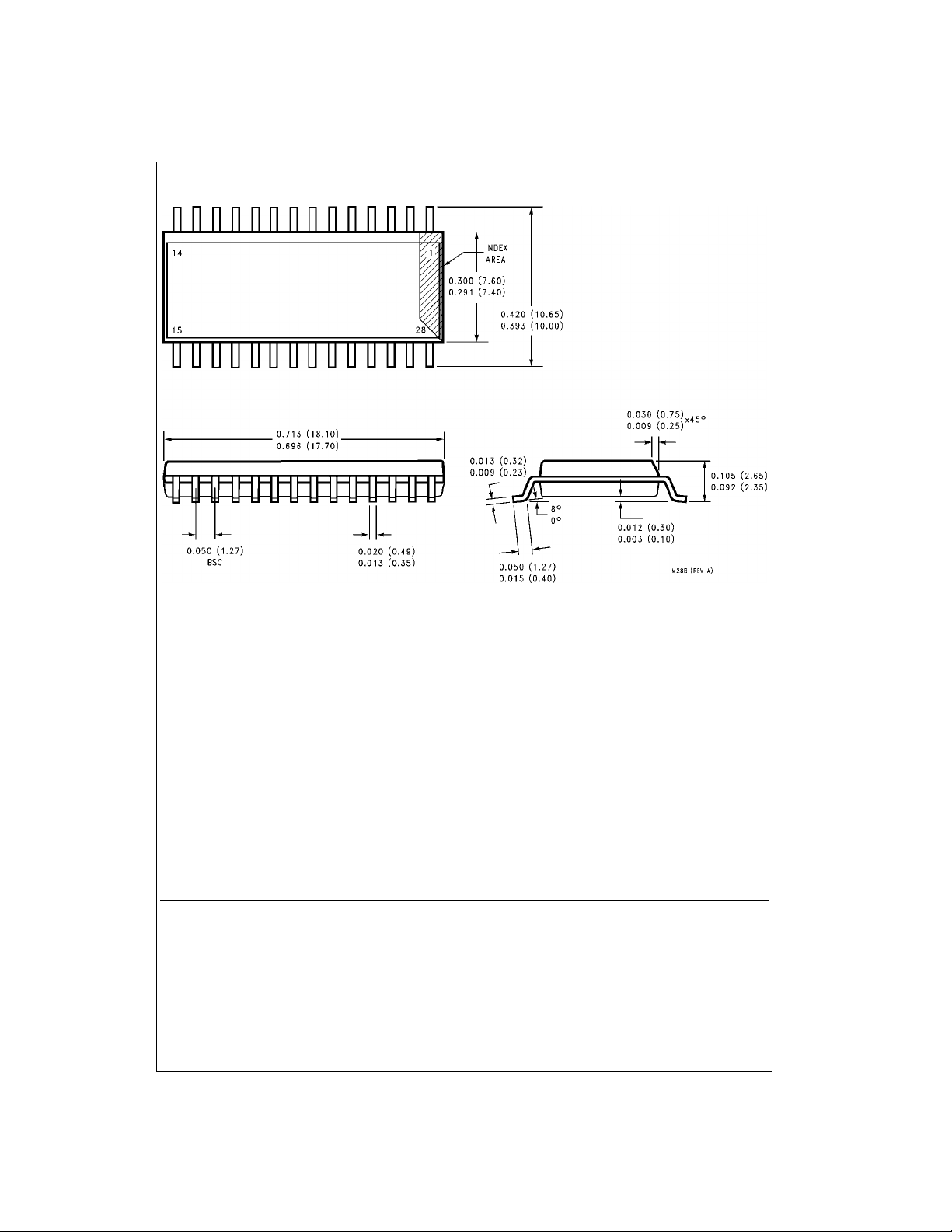
Physical Dimensions inches (millimeters) unless otherwise noted
Support)
SCANPSC110F SCAN Bridge Hierarchical and Multidrop Addressable JTAG Port (IEEE1149.1 System Test
28-Lead Small Outline Integrated Circuit (SOIC), JEDEC MS-013, 0.300 Wide)
Fairchild does not assume any responsibility for use of any circuitry described , no circuit patent licenses are implied and
Fairchild reserves the right at any time without notice to change said circuitry and specifications.
LIFE SUPPORT POLICY
FAIRCHILD’S PRODUCTS ARE NOT AUTHORIZED FOR USE AS CRITICAL COMPONENTS IN LIFE SUPPORT
DEVICES OR SYSTEMS WITHOUT THE EXPRESS WRITTEN APPROVAL OF THE PRESIDENT OF FAIRCHILD
SEMICONDUCTOR CORPORATION. As used herein:
1. Life support devices or systems are dev ic es or syste ms
which, (a) are intended for surgical implant into the
body, or (b) support or sustain life, and (c) whose failure
to perform when properly used in accordance with
instructions for use provide d in the l abe ling, can be reasonably expected to result in a significant injury to the
user.
Package Number M28B
2. A critical compo nent in any com ponen t of a life s upp ort
device or system whose failure to perform can be reasonably expected to cause the failure of the l ife support
device or system, or to affect its safety or effectiveness.
www.fairchildsemi.com
25 www.fairchildsemi.com
 Loading...