

Page 1
SCAN182373A
SCAN182373A Transparent Latch with 25
January 1993
Revised August 2000
Transparent Latch with 25
General Description
The SCAN182373A i s a high performa nce BiCMOS transparent latch featur ing separate dat a inputs organized in to
dual 9-bit bytes wit h byte-or iented latch enable and output
enable control signals. This devi ce is compliant with IEEE
1149.1 Standard Test Access Port and Boundary-Scan
Architecture with the incorporation of the defined boundaryscan test logic and test access por t con sistin g of Test Data
Input (TDI), Test Data Out (TDO), Test Mode Select (TMS),
and Test Clock (TCK).
Ω Series Resistor Outp u t s
Features
■ IEEE 1149.1 (JTAG) Compliant
■ High performance BiCMOS technology
■ 25
Ω series resistor outputs elim inate need for external
terminating resistors
■ Buffered active-low latch enable
■ 3-STATE outputs for bus-oriented applications
■ 25 mil pitch SSOP (Shrink Small Outline Package)
■ Includes CLAMP, IDCODE and HIGHZ instructions
■ Additional instructions SAMPLE-IN, SAMPLE-OUT and
EXTEST-OUT
■ Power up 3-STATE for hot insert
■ Member of Fairchild’s SCAN Products
Ordering Code:
Order Number
SCAN182373ASSC MS56A 56-Lead Shrink Small Outline Package (SSOP), JEDEC MO-118, 0.300 Wide
Devices also availab l e in Tape and Reel. Specify by appending th e s uffix let t er “X” to the ordering code.
Package
Number
Package Description
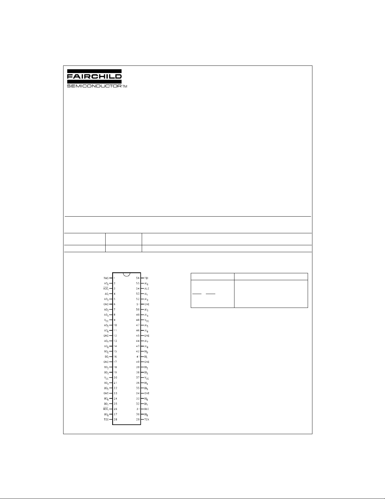
Connection Diagram Pin Descriptions
Pin Names Description
AI
, BI
(0–8)
1
(0–8)
, BOE
, BO
(0–8)
1
(0–8)
ALE, BLE Latch Enable Inputs
AOE
AO
Data Inputs
3-STATE Output Enable Inputs
3-STATE Latch Outputs
Ω
Series Resistor Outputs
© 2000 Fairchild Semiconductor Corporation DS011544 www.fairchildsemi.com
Page 2
Truth Tables
Inputs
ALE
†AOE
AI (0–8)
1
XHXZ
HLLL
SCAN182373A
HLHH
LLXAO
H = HIGH Voltage Level
L = LOW Voltage Level
X = Immaterial
Z = High Impedance
Functional Description
The SCAN182373A consists of two sets of nine D-type
latches with 3-STATE standard outputs. When the Latch
Enable (ALE or BLE) input is HIGH, data on the inputs
(AI
(0–8)
or BI
) enters the latches. In this condition the
(0–8)
latches are transparent, i.e., a latch output will change
state each time its inp ut changes. When Latch Enable is
LOW, the latches store the information that was presen t on
Logic Diagram
AO (0–8)
0
BLE
Inputs
†BOE
BI (0–8)
1
BO (0–8)
XHXZ
HLLL
HLHH
LLXBO
AO0 = Previous AO before H-to-L transition of ALE
BO
= Previous BO before H-to-L transition of BLE
0
† = Inactive-to-ac ti ve tr ans ition must occur to enable outputs upon
power-up.
0
the inputs a set-up t ime prec eding the HIGH-to- LOW transition of the Latch E nable. The 3 -STATE standard outputs
are controlled by the Outpu t En able (A OE
or BOE1) input.
1
When Output Enabl e is LOW, the standard outp uts are in
the 2-state mode. When Output E nable is HIGH, the standard outputs are in the high impedance mode, but this
does not interfere with entering new data into the latches.
Please note that this diagram is provided only for the understanding of logic operations and should not be used to estimate propagation delays.
www.fairchildsemi.com 2
Page 3
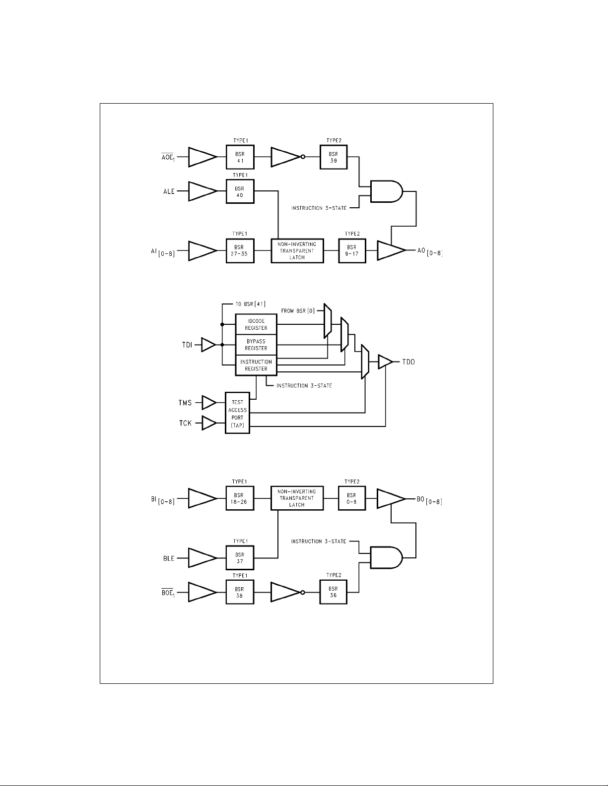
Block Diagrams
SCAN182373A
Byte-A
Tap Controller
Note: BSR stands for Boundary Sc an Register.
Byte-B
3 www.fairchildsemi.com
Page 4
Description of BOUNDARY-SCAN Circuitry
The scan cells used in the BOUNDARY- SCAN register are
one of the foll owing two types depending upon their location. Scan cell TYPE1 is intended to solely observe system
data, while TYPE2 has the additional ability to control system data.
Scan cell TYPE 1 is located on each system input pin while
SCAN182373A
scan cell TYPE2 is located at each system output pin as
well as at each of the two internal active-high output enable
signals. AOE controls the activity of the A-outputs while
BOE controls the activity of the B-outputs. Each will activate their respective outputs by loading a logic high.
The BYPASS register is a single bit shift register stage
identical to scan cell TYPE1. It captures a fixed logic low.
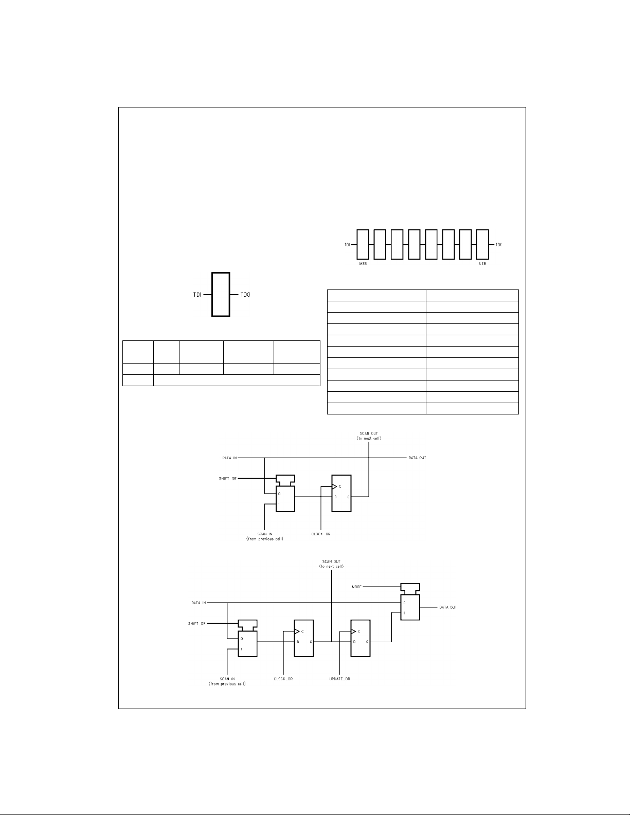
Bypass Register Scan Chain Definition
SCAN182373A Product IDCODE
(32-Bit Code per IEEE 1149.1)
Version Entity Part Manufacturer Required by
0000 111111 0000001000 00000001111 1
MSB LSB
Logic 0
Number ID 1149.1
The INSTRUCTION register is an 8-bit register which captures the default val ue of 10 000001 (SA MPLE/PR ELOAD)
during the CAPTURE-IR instr uctio n command . The ben efit
of capturing SAMPL E/PRELOAD a s the defau lt instru ction
during CAPTURE-IR is that the user is n o longer re quired
to shift in the 8-bit instruction fo r SAMP LE/PRELOA D. The
sequence of: CAPTURE-IR
will update the SAMPLE/PRELOAD instruction. For more
information refer to the section on instruction definitions.
Instruction Register Scan Chain Definition
MSB → LSB
Instruction Code Instruction
00000000 EXTEST
10000001 SAMPLE/PRELOAD
10000010 CLAMP
00000011 HIGH-Z
01000001 SAMPLE-IN
01000010 SAMPLE-OUT
00100010 EXTEST-OUT
10101010 IDCODE
11111111 BYPASS
All Others BYPASS
→ EXIT1-IR → UPDATE-IR
Scan Cell TYPE1
Scan Cell TYPE2
www.fairchildsemi.com 4
Page 5

BOUNDARY-SCAN Register
Scan Chain De finition (42 Bits in Length)
SCAN182373A
5 www.fairchildsemi.com
Page 6

SCAN182373A
Input BOUNDARY-SCAN Register
Scan Chain Definition (22 Bits in Length)
When Sample In is Active
www.fairchildsemi.com 6
Page 7

Output BOUNDARY-SCAN Register
Scan Chain De finition (20 Bits in Length)
When Sample Out and Extent Out are Active
SCAN182373A
7 www.fairchildsemi.com
Page 8

SCAN182373A
BOUNDARY-SCAN Register Definition Index
Bit No. Pin Name Pin No. Pin Type Scan Cell Type
41 AOE
1
3 Input TYPE1
40 ALE 54 Input TYPE1
39 AOE Internal TYPE2
38 BOE
1
26 Input TYPE1
Control
Signals
37 BLE 31 Input TYPE1
36 BOE Internal TYPE2
35 AI
34 AI
33 AI
32 AI
31 AI
30 AI
29 AI
28 AI
27 AI
26 BI
25 BI
24 BI
23 BI
22 BI
21 BI
20 BI
19 BI
18 BI
17 AO
16 AO
15 AO
14 AO
13 AO
12 AO
11 AO
10 AO
9AO
8BO
7BO
6BO
5BO
4BO
3BO
2BO
1BO
0BO
0
1
2
3
4
5
6
7
8
0
1
2
3
4
5
6
7
8
0
1
2
3
4
5
6
7
8
0
1
2
3
4
5
6
7
8
55 Input TYPE1
53 Input TYPE1
52 Input TYPE1
50 Input TYPE1
49 Input TYPE1
47 Input TYPE1
46 Input TYPE1
44 Input TYPE1
43 Input TYPE1
42 Input TYPE1
41 Input TYPE1
39 Input TYPE1
38 Input TYPE1
36 Input TYPE1
35 Input TYPE1
33 Input TYPE1
32 Input TYPE1
30 Input TYPE1
2 Output TYPE2
4 Output TYPE2
5 Output TYPE2
7 Output TYPE2
8 Output TYPE2
10 Output TYPE2
11 Output TYPE2
13 Output TYPE2
14 Output TYPE2
15 Output TYPE2
16 Output TYPE2
18 Output TYPE2
19 Output TYPE2
21 Output TYPE2
22 Output TYPE2
24 Output TYPE2
25 Output TYPE2
27 Output TYPE2
A-in
B-in
A-out
B-out
www.fairchildsemi.com 8
Page 9

Absolute Maximum Ratings(Note 1) Recommended Operating
Storage Temperature −65°C to +150°C
Ambient Temperature under Bias
Junction Temperature under Bias
Pin Potential to Ground Pin −0.5V to +7.0V
V
CC
Input Voltage (Note 2)
Input Current (Note 2)
−55°C to +125°C
−55°C to +150°C
−0.5V to +7.0V
−30 mA to +5.0 mA
Voltage Applied to Any Output
in Disabled or Power-Off State
in the HIGH State
−0.5V to +5.5V
−0.5V to V
Current Applied to Output
in LOW State (Max) Twice the Rated I
DC Latchup Source Current
OL
−500 mA
Over Voltage Latchup (I/O) 10V
ESD (HBM) Min 2000V
Conditions
Free Air Ambient Temperature
Supply Voltage
Minimum Input Edge Rate (
Data Input 50 mV/ns
Enable Input 20 mV/ns
CC
(mA)
Note 1: Absolute maximum ratings are values beyond which the device
may be damaged or have its useful life impaired . Functional operation
under these conditions is not implied.
Note 2: Either voltage lim it of cu rrent limit is sufficient to pr ot ec t inputs.
DC Electrical Characteristics
Symbol Parameter
V
IH
V
IL
V
CD
V
OH
V
OL
I
IH
I
BVI
I
BVIT
I
IL
V
ID
I
IH
IIL + L
I
OZH
I
OZL
I
OS
I
CEX
I
ZZ
I
CCH
I
CCL
I
CCZ
I
CCT
I
CCD
Note 3: Guaranteed not tested.
Input HIGH Voltage 2.0 V Recognized HIGH Signal
Input LOW Voltage 0.8 V Recognized LOW Signal
Input Clamp Diode Voltage Output Min −1.2 V IIN = −18 mA
HIGH Voltage Min 2.5 V IOH = −3 mA
Output LOW Voltage Min 0.8 V IOL = 15 mA
Input HIGH Current All Others Max 5 µAVIN = 2.7V (Note 3)
Input HIGH Current Breakdown Test Max 7 µAVIN = 7.0V
Input HIGH Current Breakdown Test (I/O) Max 100 µAVIN = 5.5V
Input LOW Current All Others Max −5 µAVIN = 0.5V (Note 3)
Input Leakage T est 0.0 4.75 V IID = 1.9 µA
+ I
Output Leakage Current Max 50 µAV
OZH
Output Leakage Current Max −50 V
OZL
Output Leakage Current Max 50 µAV
Output Leakage Current Max −50 µAV
Output Short-Circuit Current Max −100 −275 mA V
Output HIGH Leakage Current Max 50 µAV
Bus Drainage Test 0.0 100 µAV
Power Supply Current Max 250 µAV
Power Supply Current Max 65 mA V
Power Supply Current Max 250 µA TDI, TMS = V
Additional ICC/Input All Other Inputs Max 2.9 mA VIN = VCC −2.1V
Dynamic I
CC
TMS, TDI Max 5 µAVIN = V
TMS, TDI Max −385 µAVIN = 0.0V
TDI, TMS Inputs Max 3 mA VIN = VCC −2.1V
No Load Max 0.2 mA/ Outputs Open
V
Min Typ Max Units Conditions
CC
Min 2.0 V IOH = −32 mA
Max 5 µAVIN = V
Max −5 µAV
= 0.0V
IN
CC
CC
All Other Pins Grounded
= 2.7V
OUT
= 0.5V
OUT
= 2.7V
OUT
= 0.5V
OUT
= 0.0V
OUT
= VCC
OUT
= 5.5V
OUT
All Others Grounded
= VCC; TDI, TMS = V
Max 1.0 mA V
Max 65.8 m A V
OUT
= VCC; TDI, TMS = GND
OUT
= LOW; TDI, TMS = V
OUT
= LOW; TDI, TMS = GND
OUT
Max 1.0 mA TDI, TMS = GND
MHz One Bit Toggling, 50% Duty Cycle
SCAN182373A
−40°C to +85°C
+4.5V to +5.5V
∆V/∆t)
CC
CC
CC
9 www.fairchildsemi.com
Page 10

AC Electrical Characteristics
Normal Operation:
Symbol Parameter
t
PLH
SCAN182373A
t
PHL
t
PLH
t
PHL
t
PLZ
t
PHZ
t
PZL
t
PZH
Note 4: Voltage Range 5.0V ± 0.5V
Propagation Delay 5.0 1.2 3.7 6.5
D to Q 2.0 4.5 7.4
Propagation Delay 5.0 1.3 4.1 7.4
LE to Q 1.8 4.5 7.3
Disable Time 5.0 1.6 4.9 9.0
Enable Time 5.0 1.6 6.0 9.5
AC Operating Requirements
Normal Operation:
Symbol Parameter
t
S
Setup Time, H or L 5.0 1.7 ns
Data to LE
t
H
Hold Time, H or L 5.0 1.6 ns
LE to Data
t
W
Note 5: Voltage Range 5.0V ±0.5V
LE Pulse Width 5.0 2.3 ns
AC Electrical Characteristics
Scan Test Operation:
Symbol Parameter
t
PLH
t
PHL
t
PLZ
t
PHZ
t
PZL
t
PZH
t
PLH
t
PHL
t
PLH
t
PHL
t
PLH
t
PHL
t
PLZ
t
PHZ
t
PLZ
t
PHZ
t
PLZ
t
PHZ
t
PZL
t
PZH
t
PZL
t
PZH
t
PZL
t
PZH
Note 6: Voltage Range 5.0V ± 0.5V
Propagation Delay 5.0 3.6 5.8 8.6
TCK to TDO 4.8 7.4 10.6
Disable Time 5.0 2.7 5.6 9.0
TCK to TDO 4.0 7.1 10.9
Enable Time 5.0 5.2 8.6 12.5
TCK to TDO 3.6 6.6 10.1
Propagation Delay 3.9 6.4 9.5
TCK to Data Out during Update-DR State 5.0 5.1 8.0 11.6
Propagation Delay 4.7 7.7 11.3
TCK to Data Out during Update-IR State 5.0 5.7 9.1 13.1
Propagation Delay 5.0 5.5 9.2 13.6
TCK to Data Out during Test Logic Reset State 6.7 10.7 15.6
Disable Time 4.1 7.7 12.1
TCK to Data Out during Update-DR State 5.0 4.7 8.4 12.7
Disable Time 4.2 8.3 13.5
TCK to Data Out during Update-IR State 5.0 4.7 9.0 14.0
Disable Time 5.0 5.5 10.1 15.6
TCK to Data Out during Test Logic Reset State 6.3 10.8 16.2
Enable Time 5.8 9.6 14.2
TCK to Data Out during Update-DR State 5.0 4.3 7.7 11.7
Enable Time 6.1 11.0 16.0
TCK to Data Out during Update-IR State 5.0 4.7 9.0 13.7
Enable Time 5.0 7.3 12.5 18.3
TCK to Data Out during Test Logic Reset State 5.8 10.5 15.8
V
CC
(V)
TA = −40°C to +85°C
CL = 50 pF
(Note 4) Min Typ Max
1.8 6.0 10.7
1.0 5.0 9.3
V
CC
(V)
TA = −40°C to +85°C
= 50 pF
C
L
(Note 5) Guaranteed Minimum
V
CC
(V)
TA = −40°C to +85°C
CL = 50 pF
(Note 6) Min Typ Max
Units
ns
ns
ns
ns
Units
Units
ns
ns
ns
ns
ns
ns
ns
ns
ns
ns
ns
ns
www.fairchildsemi.com 10
Page 11

AC Operating Requirements
Scan Test Operation:
Symbol Parameter
t
S
Setup Time,
Data to TCK (Note 8)
t
H
Hold Time,
Data to TCK (Note 8)
t
S
t
H
Setup Time, H or L
AOE
1, BOE 1 to TCK (Note 9)
Hold Time, H or L
TCK to AOE 1, BOE 1 (Note 9)
t
S
Setup Time, H or L
Internal AOE, BOE, to TCK (Note 10)
t
H
Hold Time, H or L
TCK to Internal 5.0 1.8 ns
AOE, BOE (Note 10)
t
S
Setup Time
ALE, BLE (Note 11) to TCK
t
H
Hold Time
TCK to ALE, BLE (Note 11)
t
S
Setup Time, H or L
TMS to TCK
t
H
Hold Time, H or L
TCK to TMS
t
S
Setup Time, H or L
TDI to TCK
t
H
Hold Time, H or L
TCK to TDI
t
W
f
MAX
t
PU
t
DN
Note 7: Voltage Range 5.0V ± 0.5V.
Note 8: This delay represents the t iming relationship between the data input and TCK at the associat ed scan cells number ed 0-8, 9-17, 18-26 an d 27-35.
Note 9: Timing pertains to BSR 38 and 41 only.
Note 10: This delay r epresents the timing relationship betwee n AOE/BOE and TCK for scan cells 36 and 39 only.
Note 11: Timing pertains to BSR 37 and 40 only.
Note: All Input Timing Delays involving TCK are measured from the rising edge of TCK.
Pulse Width TCK H 5.0 10.3
Maximum TCK Clock Frequency 5.0 50 MHz
Wait Time, Power Up to TCK 5.0 100 ns
Power Down Delay 0.0 100 ms
VCC T
(V)
= −40°C to +85°C
A
CL = 50 pF
Units
(Note 7) Guaranteed Minimum
5.0 2.7 ns
5.0 2.4 ns
5.0 5.1 ns
5.0 1.8 ns
5.0 3.5 ns
5.0 5.1 ns
5.0 1.8 ns
5.0 7.9 ns
5.0 1.8 ns
5.0 6.0 ns
5.0 3.0 ns
L10.3
SCAN182373A
ns
Capacitance
Symbol Parameter Typ Units Conditions, T
C
IN
C
OUT
Note 12: C
Input Capacitance 5.8 pF VCC = 0.0V
Output Capacitance (Note 12) 13.8 pF VCC = 5.0V
is measured at frequency f = 1 MHz, per MIL -STD-883B, Method 3012
OUT
11 www.fairchildsemi.com
= 25°C
A
Page 12

Physical Dimensions inches (millimeters) unless otherwise noted
Series Resistor Outputs
Ω
56-Lead Shrink Small Outline Package (SSOP), JEDEC MO-118, 0.300 Wide
Package Number MS56A
SCAN182373A Transparent Latch with 25
Fairchild does not assume any responsibility for use of any circuitr y described, no circuit patent licenses are implied a nd
Fairchild reserves the right at any time without notice to change said circuitry and specifications.
LIFE SUPPORT POLICY
FAIRCHILD’S PRODUCTS ARE NOT AUTHORIZED FOR USE AS CRITICAL COMPONENTS IN LIFE SUPPORT
DEVICES OR SYSTEMS WITHOUT THE EXPRESS WRITTEN APPROVAL OF THE PRESIDENT OF FAIRCHILD
SEMICONDUCTOR CORPORATION. As used herein:
1. Life support devices or systems are device s or syste ms
which, (a) are intended for surgical implant into the
body, or (b) support or sustain life, and (c) whose failure
to perform when properly used in accordance with
instructions for use provided in the labeling, can be reasonably expected to result in a significant inju ry to the
user.
2. A critical component in any compon ent of a l ife supp ort
device or system whose failu re to perform can be reasonably expected to cause the failure of the life support
device or system, or to affect its safety or effectiveness.
www.fairchildsemi.com
www.fairchildsemi.com 12
 Loading...