

Page 1

SCAN182245A
Non-Inverting Transceiver
with 25
Ω Series Resistor Outputs
SCAN182245A Non-Inverting Transceiver with 25
December 1993
Revised August 2000
General Description
The SCAN182245 A is a high perf ormance BiCMOS b idirectional line driver featuring separate data inputs organized into dual 9-b it b y te s wit h b yte -or iented output ena ble
and direction control signals. This device is compliant with
IEEE 1149.1 Standard Test Access Port and Boundary
Scan Architecture with the incorporation of the defined
boundary-scan test logi c an d t est acce ss po rt cons i sting of
Test Data Input (TDI), Test Data Out (TDO), Test Mode
Select (TMS), and Test Clock (TCK).
Features
■ High performance BiCMOS technology
Ω series resistors in outputs eliminate the need for
■ 25
external terminating resistors
■ Dual output enable control signals
■ 3-STATE outputs for bus-oriented applications
■ 25 mil pitch SSOP (Shrink Small Outline Package)
■ IEEE 1149.1 (JTAG) Compliant
■ Includes CLAMP, IDCODE and HIGHZ instructions
■ Additional instructions SAMPL E-IN, SAM P LE -O UT and
EXTEST-OUT
■ Power Up 3-STATE for hot insert
■ Member of Fairchild’s SCAN Products
Ordering Code:
Order Number Package Number Package Description
SCAN182245ASSC MS56A 56-Lead Shrink Small Outline Package (SSOP), JEDEC MO-118, 0.300 Wide
Devices also availab l e in Tape and Reel. Specify by appending th e s uffix let t er “X” to the ordering code.
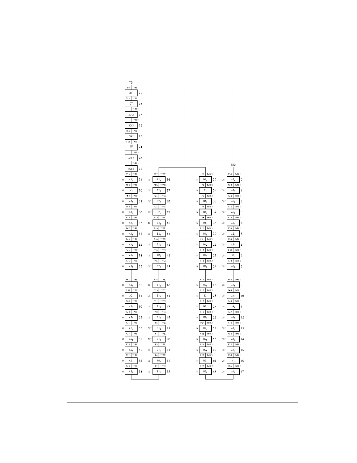
Connection Diagram Pin Descriptions
Pin Names Description
A1
(0–8)
B1
(0–8)
A2
(0–8)
B2
(0–8)
G1
, G2 Output Enable Pins (Active LOW)
DIR1, DIR2 Direction of Data Flow Pins
Side A1 Inputs or 3-STATE Outputs
Side B1 Inputs or 3-STATE Outputs
Side A2 Inputs or 3-STATE Outputs
Side B2 Inputs or 3-STATE Outputs
Ω
Series Resistor Outputs
© 2000 Fairchild Semiconductor Corporation DS011657 www.fairchildsemi.com
Page 2

Truth Tables
Inputs
G1
DIR1
A1
(0–8)
B1
(0–8)
(Note 1)
SCAN182245A
LLH
LLL
LHH
LHL
← H
← L
→ H
→ L
HXZZ
H = HIGH Voltage Level
L = LOW Voltage Level
Note 1: Inactive-to-Active transition must occur to enable outputs upon power-up.
Functional Description
The SCAN182245A consists of two sets of nine non-inverting bidirectional buffers with 3-STATE outputs and is
intended for bus-oriented applications. Direction pins (DIR1
and DIR2) LOW enables data from B Ports to A Ports,
Block Diagrams
A1, B1, G1 and DIR1
Inputs
G2
DIR2
A2
(0–8)
B2
(0–8)
(Note 1)
LLH
LLL
LHH
LHL
← H
← L
→ H
→ L
HXZZ
X = Immaterial
Z = High Impedance
when HIGH enables data from A Ports to B Ports. The Output Enable pins (G1
and G2) when HIGH disab les both A
and B Ports by placing them in a high impedance condition.
A2, B2, G2 and DIR2
Note: BSR stands for Boun dary Scan Register.
Tap Controller
www.fairchildsemi.com 2
Note: BSR stands for Bounda ry Sc an Register.
Page 3

Description of BOUNDARY-SCAN Circuitry
The scan cells used in the BOUNDARY-SCAN register are
one of the followin g two types de pending upon t heir location. Scan cell TYPE1 is intended to solely observe system
data, while TYPE2 has the additional ability to control system data.
Scan cell TYPE1 is located on each system input pin while
scan cell TYPE2 is locate d at each system output pi n as
well as at each of the two internal active-high output enable
signals. AOE controls the activity of the A-outputs while
BOE controls the activity of the B-outputs. Each will activate their respective outputs by loading a logic high.
The BYPASS register is a single bit shift register stage
identical to scan cell TYPE1. It captures a fixed logic low.
Bypass Register Scan Chain Definition
SCAN182245A Product IDCODE
(32-Bit Code per IEEE 1149.1)
Versio
Entity
n
0000 111111 000000000000000001111 1
MSB MSB
Logic 0
Part ManufacturerRequired
Number ID by 1149.1
Scan Cell TYPE1
The INSTRUCTION r egist er is a n 8-b it r egister whic h captures the default val ue of 10 000001 (SA MPLE/PRE LOAD)
during the CAPTURE-IR inst ruct ion comm and. Th e benef it
of capturing SAMPLE/PRELOAD as the default instruction
during CAPTURE-IR is that the user is no longer required
to shift in the 8-bit instruction for SAMPLE/P RELOAD . The
sequence of: CAPTURE-IR
will update the SAMPLE/PRELOAD instruction. For more
information refer to the section on instruction definitions.
→ EXIT1-IR → UPDATE-IR
Instruction Register Scan Chain Definition
MSB
→ LSB
Instruction Code Instruction
00000000 EXTEST
10000001 SAMPLE/PRELOAD
10000010 CLAMP
00000011 HIGH-Z
01000001 SAMPLE-IN
01000010 SAMPLE-OUT
00100010 EXTEST-OUT
10101010 IDCODE
11111111 BYPASS
All Others BYPASS
SCAN182245A
Scan Cell TYPE2
3 www.fairchildsemi.com
Page 4
Description of BOUNDARY-SCAN Circuitry (Continued)
BOUNDARY-SCAN Register
Scan Chain Definition (80 Bits in Length)
SCAN182245A
www.fairchildsemi.com 4
Page 5

Description of BOUNDARY-SCAN Circuitry (Continued)
Input BOUNDARY-SCAN Register
Scan Chain De finition (40 Bits in Length)
When Sample In is Active
SCAN182245A
5 www.fairchildsemi.com
Page 6

Description of BOUNDARY-SCAN Circuitry (Continued)
Output BOUNDARY-SCAN Register
Scan Chain Definition (40 Bits in Length)
When Sample Out and EXTEST-Out are Active
SCAN182245A
www.fairchildsemi.com 6
Page 7

Description of BOUNDARY-SCAN Circuitry (Continued)
BOUNDARY-SCAN Register Definition Index
Bit No. Pin Name Pin No. Pin Type Scan Cell Type Bit No. Pin Name Pin No. Pin Type Scan Cell Type
79 DIR1 3 Input TYPE1
78 G1
77 AOE
76 BOE
75 DIR2 26 Input TYPE1 31 B1
74 G2
73 AOE
72 BOE
71 A1
0
70 A1
1
69 A1
2
68 A1
3
67 A1
4
66 A1
5
65 A1
6
64 A1
7
63 A1
8
62 A2
0
61 A2
1
60 A2
2
59 A2
3
58 A2
4
57 A2
5
56 A2
6
55 A2
7
54 A2
8
53 B1
0
52 B1
1
51 B1
2
50 B1
3
49 B1
4
48 B1
5
47 B1
6
46 B1
7
45 B1
8
44 B2
0
43 B2
1
42 B2
2
41 B2
3
40 B2
4
39 B2
5
38 B2
6
37 B2
7
36 B2
8
54 Input TYPE1 34 B1
1
1
Internal TYPE2 33 B1
Internal TYPE2 32 B1
Control
Signals
31 Input TYPE1 30 B1
2
2
Internal TYPE2 29 B1
Internal TYPE2 28 B1
55 Input TYPE1
53 Input TYPE1 26 B2
52 Input TYPE1 25 B2
50 Input TYPE1 24 B2
49 Input TYPE1 23 B2
A1–in
47 Input TYPE1 22 B2
46 Input TYPE1 21 B2
44 Input TYPE1 20 B2
43 Input TYPE1 19 B2
42 Input TYPE1
41 Input TYPE1 17 A1
39 Input TYPE1 16 A1
38 Input TYPE1 15 A1
36 Input TYPE1 14 A1
A2–in
35 Input TYPE1 13 A1
33 Input TYPE1 12 A1
32 Input TYPE1 11 A1
30 Input TYPE1 10 A1
2 Output TYPE2
4 Output TYPE2 8 A2
5 Output TYPE2 7 A2
7 Output TYPE2 6 A2
8 Output TYPE2 5 A2
B1–out
10 Output TYPE2 4 A2
11 Output TYPE2 3 A2
13 Output TYPE2 2 A2
14 Output TYPE2 1 A2
15 Output TYPE2
16 Output TYPE2
18 Output TYPE2
19 Output TYPE2
21 Output TYPE2
B2–out
22 Output TYPE2
24 Output TYPE2
25 Output TYPE2
27 Output TYPE2
35 B1
27 B1
18 B2
9A1
0A2
0
1
2
3
4
5
6
7
8
0
1
2
3
4
5
6
7
8
0
1
2
3
4
5
6
7
8
0
1
2
3
4
5
6
7
8
2 Input TYPE1
4 Input TYPE1
5 Input TYPE1
7 Input TYPE1
8 Input TYPE1
10 Input TYPE1
11 Input TYPE1
13 Input TYPE1
14 Input TYPE1
15 Input TYPE1
16 Input TYPE1
18 Input TYPE1
19 Input TYPE1
21 Input TYPE1
22 Input TYPE1
24 Input TYPE1
25 Input TYPE1
27 Input TYPE1
55 Output TYPE2
53 Output TYPE2
52 Output TYPE2
50 Output TYPE2
49 Output TYPE2
47 Output TYPE2
46 Output TYPE2
44 Output TYPE2
43 Output TYPE2
42 Output TYPE2
41 Output TYPE2
39 Output TYPE2
38 Output TYPE2
36 Output TYPE2
35 Output TYPE2
33 Output TYPE2
32 Output TYPE2
30 Output TYPE2
B1–in
B2–in
A1–out
A2–out
SCAN182245A
7 www.fairchildsemi.com
Page 8

SCAN ABT Live Insertion and Power Cycling Characteristics
SCAN ABT is intended to serve in Live Insertion backplane
applications. It provides 2nd Level Isolation
1
which indicates that while external circuitry to control the output
enable pin is unnecessary, there may be a need to implement differential length backplane connector pins for V
and GND. As well, pre-bias circuitry for backplane pins
SCAN182245A
may be necessary to a void capacitive loadi ng effects during live insertion.
SCAN ABT provides control of output enable pins during
power cycling via the circuit in Figure 1. It essentially controls the G
During power-up, when V
pin until VCC reaches a known level.
n
ramps through the 0.0V to
CC
0.7V range, all interna l device circuitry is inactive, leaving
output and I/O pin s of th e device in high imp edance . From
approximately 0.8V to 1.8V V
, the Power-On-Res et cir-
CC
cuitry, (POR), in Figure 1 becomes act ive and maintains
device high impedance mode. The POR does this by providing a low from its output that resets the flip-flop The output, Q
, of the flip-flop then goes high and disables the NOR
gate from an incident al low in put on the G
, the POR circuitry becomes inactive and ceases to
V
CC
pin. After 1.8V
n
control the flip-flop. To bring the device out of high impedance, the G
input mus t r ec e i ve an i n act i ve -t o -a c ti ve t r an s i-
n
tion, a high-to-low tra nsition on G
the state of the flip-flop. With a low on the Q
flip-flop, the NOR g ate is free to allow pr opagat ion of a G
CC
signal.
During power-down, the Power-On-Reset circuitry will
become active and reset the flip-fl op at ap pro xima tel y 1.8 V
V
. Again, the Q output of the flip-flop returns to a high
CC
and disables the NOR gate fr om inputs from the G
The device will then remain in high impedance for the
remaining ramp down from 1.8V to 0.0V V
Some suggestions to help the de signer with live insertion
issues:
• The G
pin can float during power-up until the Power-
n
On-Reset circuitry becomes inactive.
• The G
pin can float on power-down only after the
n
Power-On-Reset has become active.
The description of the functionality of the Power-On-Reset
circuitry can best be described in the diagram of Figure 2.
in this case to change
n
output of the
pin.
n
.
CC
n
FIGURE 1.
1
Section 7, “Design C ons ideration for Fault Tolerant Backplanes”, Application Note AN-881.
SCAN ABT includ es additional power-o n reset circuitry not otherwise included in ABT devices.
FIGURE 2.
www.fairchildsemi.com 8
Page 9

Absolute Maximum Ratings(Note 2) Recommended Operating
Storage Temperature −65°C to +150°C
Ambient Temperature under Bias
Junction Temperature under Bias
Pin Potential to Ground Pin −0.5V to +7.0V
V
CC
Input Voltage (Note 3)
Input Current (Note 3)
−55°C to +125°C
−55°C to +150°C
−0.5V to +7.0V
−30 mA to +5.0 mA
Voltage Applied to Any Output
in the Disabled or
Power-Off State
in the HIGH State
−0.5V to +5.5V
−0.5V to V
Current Applied to Output
in LOW State (Max) Twice the Rated I
DC Latchup Source Current
OL
−500 mA
Over Voltage Latchup (I/O) 10V
ESD (HBM) Min. 2000V
Conditions
Free Air Ambient Temperature
Supply Voltage
Minimum Input Edge Rate (
Data Input 50 mV/ns
Enable Input 20 mV/ns
CC
Note 2: Absolute maximum ratings are values beyond which the device
may be damaged or have its useful life impaired . Functional operation
(mA)
under these conditions is not implied.
Note 3: Either voltage lim it or c urrent limit is sufficient to protect inputs.
DC Electrical Characteristics
Symbol Parameter
V
IH
V
IL
V
CD
V
OH
V
OL
I
IH
I
BVI
I
BVIT
I
IL
V
ID
I
IH
I
IL
I
OZH
I
OZL
I
OS
I
CEX
I
ZZ
I
CCH
I
CCL
I
CCZ
I
CCT
I
CCD
Note 4: Guaranteed not tested.
Input HIGH Voltage 2.0 V Recognized HIGH Signal
Input LOW Voltage 0.8 V Recognized LOW Signal
Input Clamp Diode Voltage Min −1.2 V IIN = −18 mA
Output HIGH Voltage Min 2.5 V IOH = −3 mA
Output LOW Voltage Min 0.8 V IOL = 15 mA
Input HIGH Current All Others Max 5 µAVIN = 2.7V (Note 4)
Input HIGH Current Breakdown Test Max 7 µAVIN = 7.0V
Input HIGH Current Breakdown Test (I/O) Max 100 µAVIN = 5.5V
Input LOW Current All Others Max −5 µAVIN = 0.5V (Note 4)
Input Leakage T est 0.0 4.75 V IID = 1.9 µA
+ I
Output Leakage Current Max 50 µAV
OZH
+ I
Output Leakage Current Max −50 µAV
OZL
Output Leakage Current Max 50 µAV
Output Leakage Current Max −50 µAV
Output Short-Circuit Current Max −100 −275 mA V
Output HIGH Leakage Current Max 50 µAV
Bus Drainage Test 0.0 100 µAV
Power Supply Current Max 250 µAV
Power Supply Current Max mA V
Power Supply Current Max 250 µA TDI, TMS = V
Additional ICC/Input
Dynamic I
CC
TMS, TDI Max 5 µAVIN = V
TMS, TDI Max −385 µAV
All Other Inputs Max 2.9 mA VIN = VCC − 2.1V
TDI, TMS inputs Max 3 mA VIN = VCC − 2.1V
No Load Max 0.2 mA/ Outputs Open
V
Min Typ Max Units Conditions
CC
Min 2.0 V IOH = −32 mA
Max 5 µAVIN = V
CC
CC
Max −5 µAVIN = 0.0V
= 0.0V
IN
All Other Pins Grounded
= 2.7V
OUT
= 0.5V
OUT
= 2.7V
OUT
= 0.5V
OUT
= 0.0V
OUT
= V
OUT
= 5.5V, All Others GND
OUT
= VCC; TDI, TMS = V
Max 1.0 mA V
Max 65.8 mA V
OUT
= VCC; TDI, TMS = GND
OUT
= LOW; TDI, TMS = V
OUT
= LOW; TDI, TMS = GND
OUT
Max 1.0 mA TDI, TMS = GND
MHz One Bit Toggling, 50% Duty Cycle
SCAN182245A
−40°C to +85°C
+4.5V to +5.5V
∆V/∆t)
CC
CC
CC
CC
9 www.fairchildsemi.com
Page 10

AC Electrical Characteristics
Normal Operation:
Symbol Parameter
t
PLH
t
PHL
SCAN182245A
t
PLZ
t
PHZ
t
PZL
t
PZH
Note 5: Voltage Range 5.0V ± 0.5V
Propagation Delay
A to B, B to A 1.5 4.4 6.5
Disable Time
Enable Time
AC Electrical Characteristics
Scan Test Operation
Symbol Parameter
t
PLH
t
PHL
t
PLZ
t
PHZ
t
PZL
t
PZH
t
PLH
t
PHL
t
PLH
t
PHL
t
PLH
t
PHL
t
PLZ
t
PHZ
t
PLZ
t
PHZ
t
PLZ
t
PHZ
t
PZL
t
PZH
t
PZL
t
PZH
t
PZL
t
PZH
Note 6: Voltage Range 5.0V ± 0.5V
Note: All Propagation Delay s involving TCK are measured from the fallin g edge of TCK.
Propagation Delay
TCK to TDO 4.2 7.7 12.1
Disable Time
TCK to TDO 3.3 7.4 12.5
Enable Time
TCK to TDO 2.8 6.8 11.5
Propagation Delay 5.0 2.8 6.3 10.7
TCK to Data Out during Update-DR State 4.5 8.2 13.0
Propagation Delay
TCK to Data Out during Update-IR State 5.0 9.3 14.8
Propagation Delay
TCK to Data Out during Test Logic Reset State 5.7 10.8 17.2
Disable Time
TCK to Data Out during Update-DR State 3.5 8.4 14.5
Disable Time
TCK to Data Out during Update-IR State 3.8 9.2 15.9
Disable Time
TCK to Data Out during Test Logic Reset State 4.2 9.9 16.6
Enable Time
TCK to Data Out during Update-DR State 3.0 7.5 13.3
Enable Time
TCK to Data Out during Update-IR State 3.9 9.0 15.4
Enable Time
TCK to Data Out during Test Logic Reset State 3.0 10.2 17.6
V
CC
(V)
TA = −40°C to +85°C
CL = 50 pF
(Note 5) Min Typ Max
5.0
5.0
5.0
V
CC
(V)
1.0 3.1 5.2
1.5 4.8 8.6
1.5 5.2 8.9
1.5 5.5 9.1
1.5 4.6 8.2
TA = −40°C to +85°C
C
= 50 pF
L
(Note 6) Min Typ Max
5.0
5.0
5.0
5.0
5.0
5.0
5.0
5.0
5.0
5.0
5.0
2.9 6.1 10.2
2.1 5.9 10.7
4.6 8.7 13.7
3.3 7.2 12.2
3.7 8.4 14.0
2.8 7.6 13.9
3.6 8.7 15.1
4.0 9.8 17.1
4.4 9.3 15.5
5.2 10.7 17.4
5.7 12.0 19.8
Units
ns
ns
ns
Units
ns
ns
ns
ns
ns
ns
ns
ns
ns
ns
ns
ns
www.fairchildsemi.com 10
Page 11

AC Operating Requirements
Scan Test Operation
Symbol Parameter
t
S
Setup Time
Data to TCK (Note 8)
t
H
Hold Time
Data to TCK (Note 8)
t
S
t
H
Setup Time, H or L
G1
, G2 to TCK (Note 9)
Hold Time, H or L
TCK to G1, G2 (Note 9)
t
S
Setup Time, H or L
DIR1, DIR2 to TCK (Note 10)
t
H
Hold Time, H or L
TCK to DIR1, DIR2 (Note 10)
t
S
Setup Time
Internal OE to TCK (Note 11)
t
H
Hold Time, H or L
TCK to Internal OE (Note 10)
t
S
Setup Time, H or L
TMS to TCK
t
H
Hold Time, H or L
TCK to TMS
t
S
Setup Time, H or L
TDI to TCK
t
H
Hold Time, H or L
TCK to TDI
t
W
Pulse Width TCK: H
L8.5
f
MAX
Maximum TCK
Clock Frequency
t
PU
Wait Time,
Power Up to TCK
t
DN
Note 7: Voltage Range 5.0V ± 0.5V
Note 8: Timing pertains to the TYPE1 BSR and TYPE2 BSR after the buffer (BSR 0–8, 9–17, 18–26, 27 –35, 36–44, 45–53, 54–62, 63–71).
Note 9: Timing pertains to BSR 74 and 78 only.
Note 10: Timing pertains to BSR 75 and 79 only.
Note 11: Timing pertains to BSR 72, 73, 76 and 77 only.
Note: All Input Timing Delays involving TCK are measured from the rising edge of TCK.
Power Down Delay 0.0 100 ms
V
CC
(V)
TA = −40°C to +85°C
CL = 50 pF
(Note 7) Guaranteed Minimum
5.0 4.8 ns
5.0 2.5 ns
5.0 4.1 ns
5.0 1.7 ns
5.0 4.2 ns
5.0 2.3 ns
5.0 3.8 ns
5.0 2.3 ns
5.0 8.7 ns
5.0 1.5 ns
5.0 6.7 ns
5.0 5.0 ns
5.0
10.2
5.0 50 MHz
5.0 100 ns
SCAN182245A
Units
ns
Capacitance
Symbol Parameter Typ Units
C
IN
C
(Note 12) Output Capacitance 13.7 pF VCC = 5.0V (An, Bn)
I/O
Note 12: C
Input Capacitance 5.9 pF VCC = 0.0V (Gn, DIRn)
is measured at frequency f = 1 MHz, per MIL-STD-883B, Method 3012.
I/O
11 www.fairchildsemi.com
Conditions, TA = 25°C
Page 12

Physical Dimensions inches (millimeters) unless otherwise noted
Series Resistor Outputs
Ω
56-Lead Shrink Small Outline Package (SSOP), JEDEC MO-118, 0.300 Wide
Package Number MS56A
SCAN182245A Non-Inverting Transceiver with 25
Fairchild does not assume any responsibility for use of any circuitr y described, no circuit patent licenses are implied a nd
Fairchild reserves the right at any time without notice to change said circuitry and specifications.
LIFE SUPPORT POLICY
FAIRCHILD’S PRODUCTS ARE NOT AUTHORIZED FOR USE AS CRITICAL COMPONENTS IN LIFE SUPPORT
DEVICES OR SYSTEMS WITHOUT THE EXPRESS WRITTEN APPROVAL OF THE PRESIDENT OF FAIRCHILD
SEMICONDUCTOR CORPORATION. As used herein:
1. Life support devices or systems are devices or syste ms
which, (a) are intended for surgical implant into the
body, or (b) support or sustain life, and (c) whose failure
to perform when properly used in accordance with
instructions for use provided in the labeling, can be reasonably expected to result in a significant inju ry to the
user.
2. A critic al com ponent in any compon ent of a life supp ort
device or system whose failu re to perform can be reasonably expected to cause the failure of the life support
device or system, or to affect its safety or effectiveness.
www.fairchildsemi.com
www.fairchildsemi.com 12
 Loading...