

Page 1

INTEGRATED CIRCUITS
DATA SH EET
SAA5355
Single-chip colour CRT controller
(FTFROM)
Product specification
File under Integrated Circuits, IC02
March 1986
Page 2

Philips Semiconductors Product specification
Single-chip colour CRT controller
SAA5355
(FTFROM)
GENERAL DESCRIPTION
The SAA5355 FTFROM (Five-Two-Five-ROM) is a single-chip VLSI NMOS crt controller capable of handling the display
functions required for a 525-line, level-3 videotex decoder. Only minimal hardware is required to produce a videotex
terminal using FTFROM the simplest configuration needs just a microcontroller and 4 Kbytes of display memory.
Features
• Minimal additional hardware required
• Screen formats of 40/80 character by 1-to-25 row display
• 512 alphanumeric or graphical characters on-chip or extendable off-chip
• Serial attribute storage (STACK) and parallel attribute storage
• Dynamically redefinable character (DRCS) capability over full field
• Interfaces with 8/16-bit microprocessors with optional direct memory access
• On-chip scroll map minimizes data to be transferred when scrolling
• 32 on-screen colours redefinable from a palette of 4096
• Three on-chip digital-to-analogue converters which compensate for crt non-linearity
• Memory interface capable of supporting multi-page terminals. FTFROM can access up to 128 Kbytes of display
memory
• Programmable cursor
• Programmable local status row
• Three synchronization modes:
stand-alone built-in oscillator operating with an external 6,041957 MHz crystal
simple slave directly synchronized from the source of text composite sync
phase-locked slave indirect synchronization allows picture-in-text displays (e.g. VCR/VLP video with text overlay)
• On-chip timing with composite sync output
• Zoom feature which allows the height of any group of rows to be increased to enhance legibility
PACKAGE OUTLINE
40-lead DIL; plastic (SOT129); SOT 129-1; 1996 November 18.
March 1986 2
Page 3

Philips Semiconductors Product specification
Single-chip colour CRT controller
(FTFROM)
SAA5355
March 1986 3
Fig.1 Block diagram.
Page 4

Philips Semiconductors Product specification
Single-chip colour CRT controller
SAA5355
(FTFROM)
PINNING
1V
2
3
4 to 19 A16 to A1/
20 V
21 REF Analogue reference input.
22 B
24 R
25
26
27 CLKO 12 MHz clock output for hard-copy dot synchronization (referenced to output
28 SAND Sandcastle feedback output for SAA5230 teletext video processor or other circuit.
29 F1/F6 1,00699 MHz or 6,041957 MHz output.
30 F6 6,041957 MHz clock input (e.g. from SAA5230). Internal a.c. coupling is provided.
31 VCS/OSCO Video composite sync input (e.g. from SAA5230) for phase reference of vertical
32
33
34
35
36
37
38
39 R/
40 V
SS(1)
BUFEN Buffer enable input to the 8-bit link-through buffer.
RE Register enable input. This enables A1 to A6 and UDS as inputs,
D15 to D0
SS(2)
VDS Switching output for dot, screen (row), box and window video data; for use when
OD Output disable causing R, G, B and VDS outputs to go to high-impedance state.
TCS Text composite sync input/output depending on master/slave status.
FS/DDA Field sync pulse output or defined-display-area flag output (both referenced to
UDS Upper data strobe input/output.
LDS Lower data strobe output.
DTACK Data transfer acknowledge (open drain output).
BR Bus request to microprocessor (open drain output).
AS Address strobe output to external address latches.
W(S/R) Read/write input/output. Also serves as send/receive for the link-through buffer.
DD
Ground (0 V).
and D8 to D15 as input/outputs.
Multiplexed address and data bus input/outputs. These pins also function as the
8-bit link-through buffer.
Ground (0 V).
Analogue outputs (signals are gamma-corrected).23 G
video signal is present (e.g. from tv , VLP, alpha + photographic layer). This output
is LOW for tv display and HIGH for text and will interface directly with a number of
colour decoder ICs (e.g. TDA3563, TDA3562A).
Can be used at dot-rate.
dots).
Used when the display must be locked to the video source (e.g. VLP).
The phase-lock part of the sandcastle waveform can be disabled to allow
free-running of the SAA5230 phase-locked loop.
display timing when locking to a video source (e.g. VLP) or, in stand-alone sync
mode, output from internal oscillator circuit (fixed frequency).
output dots).
Positive supply voltage (+ 5 V).
March 1986 4
Page 5

Philips Semiconductors Product specification
Single-chip colour CRT controller
(FTFROM)
SAA5355
Fig.2 Pinning diagram.
RATINGS
Limiting values in accordance with the Absolute Maximum System (IEC 134)
Supply voltage range (pin 40) V
Maximum input voltage (except F6,
Maximum input voltage (F6,
TCS) V
TCS, REF) V
Maximum input voltage (REF) V
Maximum output voltage V
Maximum output current I
Operating ambient temperature range T
Storage temperature range T
Outputs other than CLKO, OSCO, R, G, B, and
VDS are short-circuit protected.
March 1986 5
DD
Imax
lmax
REF
Omax
Omax
amb
stg
−0,3 to + 7,5 V
−0,3 to + 7,5 V
−0,3 to + 10,0 V
−0,3 to + 3,0 V
−0,3 to + 7,5 V
10 mA
−20 to + 70 °C
−55 to + 125 °C
Page 6

Philips Semiconductors Product specification
Single-chip colour CRT controller
SAA5355
(FTFROM)
CHARACTERISTICS
= 5 V ± 5%; VSS = 0 V; T
V
DD
PARAMETER SYMBOL MIN. TYP. MAX. UNIT
SUPPLY
Supply voltage (pin 40) V
Supply current (pin 40) I
INPUTS
F6 (note 1)
Slave modes
(Fig.3)
Input voltage (peak-to-peak value) V
Input peaks relative to
50% duty factor ±V
Input leakage current at
V
= 0 to 10 V; T
I
= 25 °CI
amb
Input capacitance C
Stand-alone mode
(Fig.4)
Series capacitance of crystal C
Parallel capacitance of crystal C
Resonance resistance of crystal R
Gain of circuit G −−note 2 V/V
= −20 to + 70 °C; unless otherwise specified.
amb
DD
DD
I (p-p)
P
LI
I
1
0
r
4,75 5,0 5,25 V
−−350 mA
1,0 − 7,0 V
0,2 − 3,5 V
−−20 µA
−−12 pF
− 28 − fF
− 7,1 − pF
−−60 Ω
BUFEN, RE, OD
Input voltage LOW V
Input voltage HIGH V
IL
IH
0 − 0,8 V
2,0 − 6,5 V
Input current at
V
= 0 to VDD+ 0,3 V; T
I
Input capacitance C
= 25 °CI
amb
I
I
−10 −+10 µA
−−7pF
REF (Fig.5)
Input voltage V
REF
0 1 to 2 2,7 V
Resistance (pin 21 to pin 20) with
REF supply and R, G, B outputs OFF R
REF
− 125 −Ω
OUTPUTS
SAND
Output voltage high level at
= 0 to −10 µAV
I
O
OH
4,2 − V
Output voltage intermediate level at
I
= −10 to +10 µAV
O
OI
1,3 2,0 2,7 V
Output voltage low level at
IOH = 0,2 mA V
Load capacitance C
OL
L
0 − 0,2 V
−−130 pF
DD
V
March 1986 6
Page 7

Philips Semiconductors Product specification
Single-chip colour CRT controller
SAA5355
(FTFROM)
PARAMETER SYMBOL MIN. TYP. MAX. UNIT
F1/F6, CLKO, DDA/FS
Output voltage HIGH at
IOH = −200 µAV
Output voltage LOW at I
= 3,2 mA V
OL
Load capacitance C
OH
OL
L
LDS, AS
Output voltage HIGH at
IOH= −200 µAV
Output voltage LOW at I
= 3,2 mA V
OL
Load capacitance C
OH
OL
L
DTACK, BR (open drain outputs)
Output voltage LOW at I
Load capacitance C
Capacitance (OFF state) C
= 3,2 mA V
OL
OL
L
OFF
R, G, B (note 3)
Output voltage HIGH (note 4) at
= −100 µA; V
I
OH
Output voltage LOW at I
Output resistance during line blanking R
Output capacitance (OFF state) C
= 2,7 V V
REF
= 2 mA V
OL
OH
OL
OBL
OFF
Output leakage current (OFF state)
at VI = 0 to VDD+ 0,3 V;
T
= 25 °CI
amb
OFF
VDS
Output voltage HIGH at I
Output voltage LOW at I
Output voltage LOW at I
= −250 µAV
OH
= 2 mA V
OL
= 1 mA V
OL
OH
OL
OL
Output leakage current (OFF state)
at V
= 0 to VDD+ 0,3 V;
I
= 25 °CI
T
amb
OFF
INPUT/OUTPUTS
2,4 − V
DD
0 − 0,4 V
−−50 pF
2,4 − V
DD
0 − 0,4 V
−−200 pF
0 − 0,4 V
−−150 pF
−−7pF
2,4 −−V
−−0,4 V
−−150 Ω
−−12 pF
−10 −+10 µA
2,4 − V
DD
0 − 0,4 V
0 − 0,2 V
−10 −+10 µA
V
V
V
VCS/OSCO
Input voltage HIGH V
Input voltage LOW V
Input current (output OFF) at
VI = 0 to VDD+ 0,3 V;
= 25 °CI
T
amb
Input capacitance C
Load capacitance C
March 1986 7
IH
IL
I
I
L
2,0 − 6,0 V
0 − 0,8 V
−10 −+10 µA
−−10 pF
−−50 pF
Page 8

Philips Semiconductors Product specification
Single-chip colour CRT controller
(FTFROM)
PARAMETER SYMBOL MIN. TYP. MAX. UNIT
TCS
Input voltage HIGH V
Input voltage LOW V
IH
IL
Input current at
V
= 0 to VDD+ 0,3 V;
I
=25°CI
T
amb
Input capacitance C
I
I
Output voltage HIGH at
I
= −200 to 100 µAV
OH
Output voltage LOW at V
= 3,2 mA V
OL
Load capacitance C
A1/D0 to A16/D15,
UDS, R/W
Input voltage LOW V
Input voltage HIGH V
OH
OL
L
IL
IH
Input current at
V
= 0 to VDD+ 0,3 V;
I
T
=25°CI
amb
Input capacitance C
Output voltage HIGH at I
Output voltage LOW at I
= −200 µAV
OH
= 3,2 mA V
OL
Load capacitance C
I
I
OH
OL
L
TIMING (note 5)
3,5 − 10,0 V
0 − 1,5 V
−10 −+10 µA
−−10 pF
2,4 − 6,0 V
0 − 0,4 V
−−50 pF
0 − 0,8 V
2,0 − 6,0 V
−10 −+10 µA
−−10 pF
2,4 − V
0 − 0,4 V
−−200 pF
SAA5355
DD
V
F6 (Fig.3)
Rise and fall times t
Frequency f
March 1986 8
r
F6
, t
f
10 − 80 ns
5,9 − 6,1 MHz
Page 9

Philips Semiconductors Product specification
Single-chip colour CRT controller
(FTFROM)
PARAMETER SYMBOL MIN. TYP. MAX. UNIT
CLKO, F1/F6, R, G, B, VDS
FS/DDA, OD (notes 6, 7 and Fig.6)
CLKO HIGH time t
CLKO LOW time t
CLKO rise and fall times t
CLKO HIGH to R, G, B,
R, G, B,
VDS valid to CLKO rise t
CLKO HIGH to R, G, B,
CLKO HIGH to R, G, B,
after
OD fall t
Skew between outputs R, G, B,
R, G, B,
VDS rise and fall times tVr, t
CLKO HIGH to R, G, B,
after
OD rise t
CLKO HIGH to
FS/DDA change t
FS/DDA valid to CLKO rise t
F1 HIGH time (note 8) t
F1 LOW time (note 8) t
F6 HIGH time t
F6 LOW time t
OD to CLKO rise set-up t
OD to CLKO HIGH hold t
MEMORY ACCESS TIMING
(notes 9, 10 and Fig.7)
VDS change t
VDS valid t
VDS floating
VDS t
VDS active
CLKH
CLKL
CLKr
t
CLKf
VCH
VOC
COV
FOD
VS
UOD
DCH
DOC
F1H
F1L
F6H
F6L
ODS
ODH
SAA5355
25 −−ns
15 −−ns
−−10 ns
10 −−ns
10 −−ns
−−60 ns
0 − 30 ns
−−20 ns
Vf
−−30 ns
0 − 60 ns
10 − 60 ns
5 −−ns
− 500 − ns
− 500 − ns
− 83 − ns
− 83 − ns
−−45 ns
−−0ns
UDS, LDS, AS
Cycle time t
UDS HIGH to bus-active for address output t
Address valid set-up to
Address valid hold from
Address float to
UDS fall t
AS fall t
AS LOW t
AS LOW to UDS fall delay t
UDS, LDS HIGH time t
UDS, LDS LOW time t
AS HIGH time t
AS LOW time t
March 1986 9
cyc
SAA
ASU
ASH
AFS
ATD
HDS
LDS
HAS
LAS
− 500 − ns
75 −−ns
20 −−ns
20 −−ns
0 −−ns
50 −−ns
220 −−ns
200 −−ns
125 −−ns
320 −−ns
Page 10

Philips Semiconductors Product specification
Single-chip colour CRT controller
(FTFROM)
PARAMETER SYMBOL MIN. TYP. MAX. UNIT
AS LOW to UDS HIGH t
Data valid set-up to
Data valid hold from
UDS HIGH to AS rise delay t
AS LOW to data valid t
Link-through buffers
(notes 9, 10 and Fig.8)
BUFEN LOW to output valid t
Link-through delay time t
Input data float prior to direction change t
Output float after direction change t
Output float after
Microprocessor READ from FTFROM
(Fig.9)
R/
W HIGH set-up to UDS fall t
UDS LOW to returned-data access time t
RE LOW to returned data access time t
Data valid to
DTACK LOW to UDS rise t
UDS HIGH to DTACK rise t
UDS HIGH to address hold t
UDS HIGH to data hold t
UDS HIGH to RE rise t
UDS HIGH to R/W fall t
UDS LOW to DTACK LOW t
Address valid to
UDS rise t
UDS HIGH t
BUFEN HIGH t
DTACK LOW delay t
UDS fall t
AUH
DSU
DSH
UAS
AFA
BEA
LTD
IFR
OFR
BED
RUD
UDA
REA
DTL
DLU
DTR
DSA
DSH
SRE
UDR
DSD
AUL
SAA5355
305 −−ns
30 −−ns
0 −−ns
0 − 15 ns
−−275 ns
−−100 ns
−−85 ns
0 −−ns
−−60 ns
−−60 ns
0 −−ns
−−210 ns
−−210 ns
40 −−ns
0 −−ns
0 − 75 ns
10 −−ns
10 −−ns
10 −−ns
0 −−ns
250 − 350 ns
0 −−ns
March 1986 10
Page 11

Philips Semiconductors Product specification
Single-chip colour CRT controller
(FTFROM)
PARAMETER SYMBOL MIN. TYP. MAX. UNIT
Microprocessor WRITE to FTFROM (Fig.10)
Write cycle time (note 11) t
R/
W LOW set-up to UDS fall t
RE LOW to UDS fall t
Address valid to
UDS LOW time t
Data valid to
UDS LOW to DTACK LOW t
UDS HIGH to DTACK rise t
UDS HIGH to data hold t
UDS HIGH to address hold t
UDS HIGH to RE rise t
UDS HIGH to R/W rise t
F1/F6 to memory access cycle (Fig.11)
UDS HIGH to F6 (component of F1/F6) rise t
F6 (component of F1/F6) HIGH to
SYNCHRONIZATION and BLANKING
UDS fall t
UDS rise t
UDS rise t
WCY
WUD
RES
ASS
LUS
DSS
DTA
DTR
DSH
DSA
SRE
UDW
UF6
F6U
SAA5355
500 −−ns
0 −−ns
30 −−ns
30 −−ns
100 −−ns
80 −−ns
0 − 60 ns
0 − 75 ns
10 −−ns
10 −−ns
10 −−ns
0 −−ns
20 −−ns
40 −−ns
TCS, SAND, FS/DDA
See Fig.12 for timing relationships
and Fig.13 for vertical sync and
blanking waveforms.
Notes to the characteristics
1. Pin 30 must be biased externally.
2. Value under investigation
3. 16-level analogue voltage outputs.
4. Output voltage guaranteed when programmed for top level.
5. All timings are related to a 6,00 MHz clock.
6. CLKO, R, G, B, F1/F6, VDS: CL= 25 pF.
FS/DDA: CL = 50 pF
7. CLKO, F1/F6, VDS, FS/DDA: reference levels = 0,8 to 2,0 V
R, G, B: reference levels = 0,8 to 2,0 V with V
REF
= 2,7 V
8. These times may momentarily be reduced to a nominal 83 ns in slave-sync mode at the moment of
re-synchronization.
9. CL = 150 pF.
10. Reference levels = 0,8 to 2,0 V.
11. Microprocessor write cycle times of less than 500 ns are permitted but often result in Wait States being generated,
the precise timing of DTACK will then depend on the internal synchronization time.
March 1986 11
Page 12

Philips Semiconductors Product specification
Single-chip colour CRT controller
(FTFROM)
Fig.3 F6 input waveform.
SAA5355
(1) for 525-line operation, frequency = 6,041957 MHz.
Fig.4 (a) Oscillator circuit for SAA5355 stand-alone sync mode and (b) equivalent circuit of crystal at resonance
(see characteristics for values).
Fig.5 Circuit arrangement giving one-of-sixteen reference voltage levels for the R, G or B analogue outputs.
March 1986 12
Page 13

Philips Semiconductors Product specification
Single-chip colour CRT controller
(FTFROM)
SAA5355
Fig.6 Video timing.
Fig.7 Memory access timing.
March 1986 13
Page 14

Philips Semiconductors Product specification
Single-chip colour CRT controller
(FTFROM)
SAA5355
Fig.8 Timing of link-through buffers.
Fig.9 Timing of microprocessor read from FTFROM.
March 1986 14
Page 15

Philips Semiconductors Product specification
Single-chip colour CRT controller
(FTFROM)
SAA5355
Fig.10 Timing of microprocessor write to FTFROM.
Fig.11 Timing of F1/F6 to memory access cycle.
March 1986 15
Page 16

March 1986 16
Philips Semiconductors Product specification
Single-chip colour CRT controller
(FTFROM)
Fig.12 Timing of synchronization and blanking outputs; all timings are nominal and assume fF6 = 6,041957 MHz.
SAA5355
Page 17
March 1986 17
Philips Semiconductors Product specification
Single-chip colour CRT controller
(FTFROM)
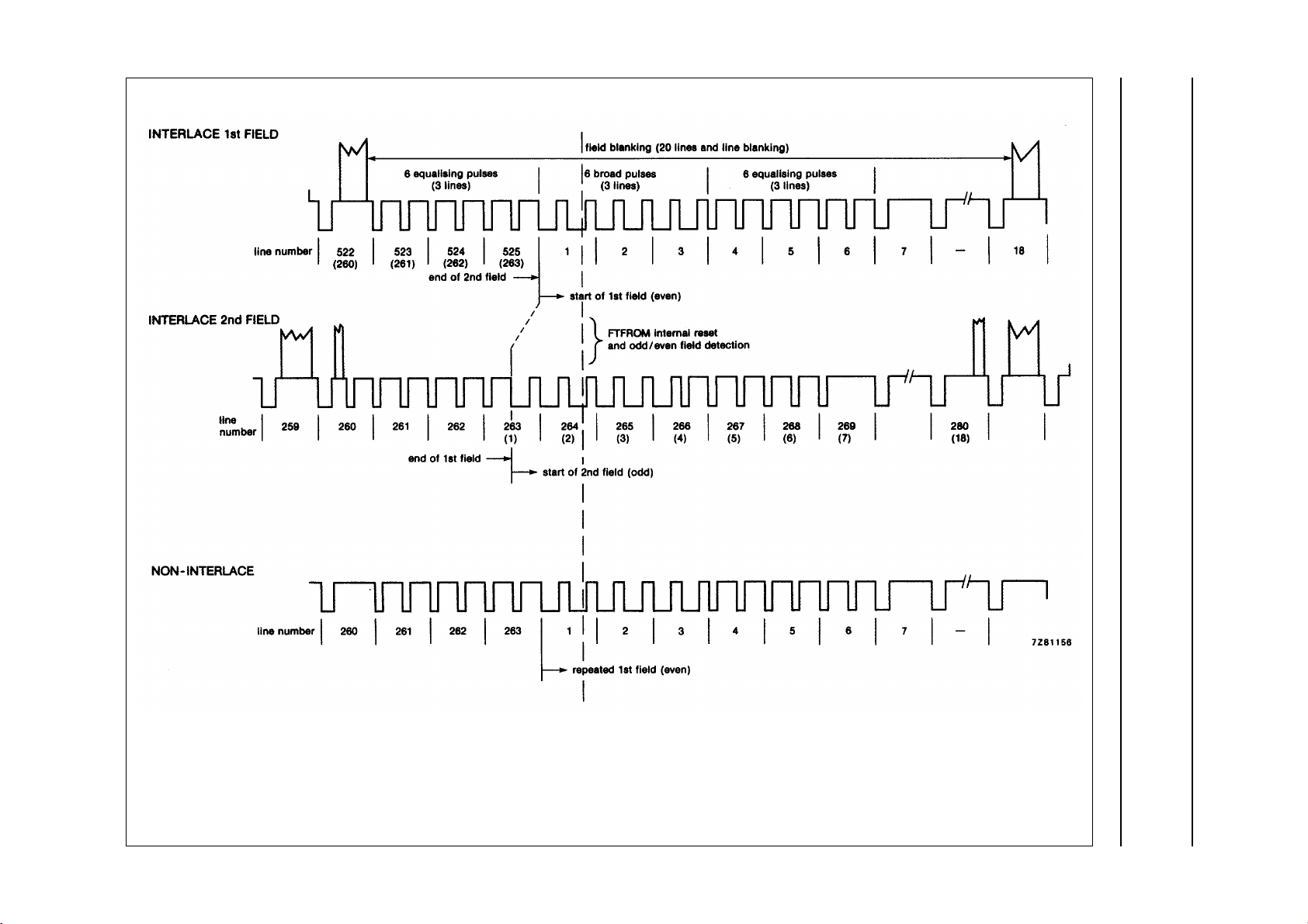
Fig.13 Vertical synchronization and blanking waveforms; separation of broad pulses = 4,717 µs; equalizing pulse widths = 2,23 µs.
SAA5355
Page 18

Philips Semiconductors Product specification
Single-chip colour CRT controller
SAA5355
(FTFROM)
APPLICATION INFORMATION
More detailed application information is available on request
BASIC VIDEOTEX DECODER CONFIGURATION
A basic, practical decoder configuration is shown in Fig.14, reference should also be made to the block diagram Fig.1.
Fig.14 Basic videotex decoder configuration.
Character and attribute data is fetched from the external memory, processed by the row buffer fill logic according to the
stack coding scheme (in stack mode) and then fed into one half of the dual display row buffer. The data fetch process
takes place during one line-flyback period (per row) and, since time is required to complete the fill, the other half of the
dual row buffer is used for display. The row buffers exchange functions on alternate rows each holds the 40 columns
of 32 bits required to define explicitly every character in a row.
The addresser is used for row buffer filling and for fetching screen colours, and during the display time it is also used for
addressing DRCS characters.
Timing
The timing chain operates from an external 6,041957 MHz clock or an on-chip fixed-frequency crystal oscillator.
The basic video format is 40 characters per row, 20/21 rows per page and 10 video lines per row. FTFROM will also
operate with 25 rows per page and 9 video lines per row.
The display is generated to the normal 525-line/59,94 Hz scanning standard (interlaced or non-interlaced). In addition to
composite sync (pin 32) for conventional timebases, a clock output at approximately 1 MHz or 6 MHz (pin 29) is
available for driving other devices, and a clock output (pin 27) is available for hard-copy dot synchronization.
A defined-display-area timing signal (pin 33) simplifies the application of external peripherals such as a light pen;
this signal is nominally coincident with the character dot information.
March 1986 18
Page 19

Philips Semiconductors Product specification
Single-chip colour CRT controller
SAA5355
(FTFROM)
Character generation
FTFROM supports eight character tables, each of (nominally) 128 characters. Four tables are in on-chip ROM and
contain fixed characters and four are stored in an external RAM. The fixed character tables (Tables 0 to 3), shown in Figs
15 and 16, are applicable to 10-lines-per-row applications. For 9 lines per row applications, the characters will be as
shown but with the last line removed from alpha characters and line 5 (labelling 0 to 9) removed from mosaic and line
drawing characters.
(a) (b)
Fig.15 On-chip characters: (a) Table 0; (b) Table 1.
March 1986 19
Page 20

Philips Semiconductors Product specification
Single-chip colour CRT controller
(FTFROM)
SAA5355
(a) (b)
Fig.16 On-chip characters: (a) Table 2; (b) Table 3.
The 128 most commonly used characters are contained in Table 0, these are the standard upper and lower-case letters
of the Roman alphabet, numerals, punctuation and the more common accented characters. In normal text transmission,
Table 0 is used most of the time. Table 1 contains other accented characters. Miscellaneous characters, mathematical
symbols, the line drawing character set and accents without associated symbols are contained in Table 2.
Table 3 contains the block mosaics for the basic alpha-mosaic service and also the new smooth mosaics.
The four tables stored in the external RAM (Tables 4 to 7) are used for DRCS.
March 1986 20
Page 21

Philips Semiconductors Product specification
Single-chip colour CRT controller
SAA5355
(FTFROM)
Scroll map
The scroll map uses a 26-byte area of on-chip RAM and functions in association with the timing chain. It maps the scan
row on to the fetched memory row so allowing the stored page to be displayed in any row order. For each row, a 1-byte
pointer to the display memory row is stored in the scroll map. This allows scrolling without the need for data transfer to,
or from, side storage.
Additional control bits are stored, allowing 1 to 25 rows to be displayed at any location on the screen.
Colour map and digital-to-analogue converters
The colour map RAM contains thirty-two 12-bit words that are loaded by the microprocessor and read out in three 4-bit
groups at pixel rate. Each group is fed to a non-linear (gamma-corrected) D-A converter. The resulting R, G and B outputs
are low-impedance with peak-to-peak amplitudes controlled by the reference voltage applied at pin 21.
Cursor
The cursor is available in the stack mode. Its position, character code, character table, foreground colour, background
colour, lining and flash attributes are all software programmable via internal register bits.
NON-VIDEOTEX APPLICATIONS
For non-Videotex applications, the device will also support the following operating modes:
Explicit fill mode. An alternative 40 character/rows mode which does not use the memory compression technique of
stack coding. More display memory is required but there are no limitations on the number of display attribute changes
per row.
80 characters/rows mode. When operating with 80 characters per row, the available display attributes are eight
foreground colours, eight (potentially different) background colours (including transparent) as well as underline and blink.
Full field DRCS mode. This mode is not mutually exclusive to the explicit fill and 80 characters/rows modes but rather
the available DRCS memory is expanded so that the whole screen can be covered, thus enabling a ‘bit map’. All
ROM-based characters and all display attributes remain available.
MICROPROCESSOR and RAM BUS INTERFACE
Three types of data transfer take place at the bus interface:
• FTFROM fetches data from the display memory
• The microprocessor reads from, or writes to, FTFROM’s internal register map
• The microprocessor accesses the display memory
FTFROM access to display memory (Figs 17 and 18)
FTFROM accesses the external display memory via a 16-bit multiplexed address and data bus with a cycle time of
496,5 ns (F6 = 6,041957 MHz). The address strobe (
into octal latches (74LS373). The display data is stored in bytes of upper (most-significant) and lower (least-significant)
display information and is always fetched in pairs of bytes (upper + lower = 16 bits). The upper and lower display RAM
sections are enabled simultaneously by the upper and lower data strobes (respectively UDS andLDS) which are always
asserted together to fetch a 16-bit word. The read/write control R/W is included although FTFROM only reads from the
display memory.
AS) signal from FTFROM flags the bus cycle and writes the address
March 1986 21
Page 22

Philips Semiconductors Product specification
Single-chip colour CRT controller
(FTFROM)
(1) 74LS373 octal transparent latch (3-state)
SAA5355
Fig.17 Simply RAM interface circuit for display memory access.
Fig.18 Bus timing for display memory access.
March 1986 22
Page 23

Philips Semiconductors Product specification
Single-chip colour CRT controller
SAA5355
(FTFROM)
The display memory organization uses the word/byte addressing convention adopted for the SCN68000 microprocessor
series. Data fetched on the 16-bit bus is considered in terms of bytes where the even numbered bytes use the upper
(most-significant) part of the bus as shown in Fig.19. The word addresses are numerically the same as the upper byte
that they contain - there are no odd-numbered word addresses.
Fig.19 Display memory word/byte organization.
Warning time
As FTFROM is a real-time display device, it must have direct access to the display memory with priority over the
microprocessor and other peripheral devices. This is achieved by FTFROM issuing a bus request (
duration of the memory access plus a programmable advance warning time which allows the microprocessor to complete
its current bus cycle.
In systems where the buses of the microprocessor and FTFROM are intimately connected (connected systems),BR may
be used to suspend all microprocessor activity so that FTFROM can act as a dedicated DMA controller. In systems where
the two buses are separated by buffers (disconnected systems), BR may be used either to generate an interrupt or as a
direct signal. To these ends, the warning time between the assertion of BR and the beginning of FTFROM’s bus activity
is programmable to be between 0 and 22,84 µs.
BR) signal for the
March 1986 23
Page 24

Philips Semiconductors Product specification
Single-chip colour CRT controller
SAA5355
(FTFROM)
Microprocessor access to register map
FTFROM has a set of internal registers which, when memory-mapped, behave as an 8-bit wide RAM connected to the
upper part of the data bus (Fig.20). The control signals UDS and R/W are reversed to become inputs and the register
map is enabled by the signal RE. Addresses are input via the lower part of the bus. A data transfer acknowledge signal
(DTACK) indicates to the microprocessor that the data transfer is complete.
Fig.20 Microprocessor access to register map.
The main data and address paths used in a connected 68000 interface are shown in Fig.21. The outputs from the octal
latches (74LS373) are enabled only when the 68000 has made the bus available in response to a bus request (
When the register map is accessed data is transferred via the upper part of the bus and the microprocessor’s low-order
address is passed to FTFROM via the octal buffers (74LS244). At the same time the bidirectional buffers (74LS245)
disable the signals from the low order data bus of the 68000.
The buffers ‘244 and ‘245 may be omitted in a 16-bit write-only configuration where the least-significant data byte is
interpreted by FTFROM as an address. Here it will generally be necessary for the microprocessor to hold a (readable)
‘master copy’ of FTFROM’s scroll map contents at a location in its main memory.
8-bit microprocessors
Although the control bus is optimised for the SCN68000 16-bit microprocessor unit, FTFROM will operate with a number
of widely differing industry-standard 8, 16 or more-bit microprocessors or microcontrollers (e.g. SCN68008, MAB8051).
The interfacing of 8-bit microprocessors to the 16-bit wide display memory is made simple by FTFROM’s on-chip
link-through buffer which provides the microprocessor with bidirectional access to the lower (odd) half of the memory.
The link-through buffer is enabled by the buffer-enable signal
signal S/R.
The main data and address paths used in a connected 8-bit microprocessor system are shown in Fig.22. The interface
is similar to that of the 16-bit system but here the display memory does not receive A0 as an address, rather A0 is used
as the major enabling signal for BUFEN (enables when HIGH).
BUFEN, and the send/receive direction is controlled by the
BR).
March 1986 24
Page 25

Philips Semiconductors Product specification
Single-chip colour CRT controller
(FTFROM)
SAA5355
(1) 74LS373 octal transparent latch (3-state)
(2) 74LS244 octal buffer (3-state)
(3) 74LS245 octal transceiver (3-state)
(4) SCN6800 microprocessor unit
Fig.21 Connected 16-bit microprocessor system.
March 1986 25
Page 26

Philips Semiconductors Product specification
Single-chip colour CRT controller
(FTFROM)
SAA5355
(1) 74LS373 octal transparent latch (3-state)
(2) 74LS244 octal buffer (3-state)
Fig.22 Connected 8-bit microprocessor system.
March 1986 26
Page 27

Philips Semiconductors Product specification
Single-chip colour CRT controller
SAA5355
(FTFROM)
Disconnected systems
For many applications it may be desirable to disconnect FTFROM and the display memory from the microprocessor and
its ROM, RAM and other peripherals by using isolating buffers as shown in Fig.23. The two parts of the system then
operate independently and communicate only when the microprocessor accesses FTFROM’s register map or the display
memory.
(1) 74LS373 octal transparent latch (3-state)
(2) 74LS244 octal buffer (3-state)
(3) 74LS245 octal bus transceiver (3-state)
Fig.23 Disconnected 8-bit system.
March 1986 27
Page 28

Philips Semiconductors Product specification
Single-chip colour CRT controller
SAA5355
(FTFROM)
Synchronization
Stand-alone mode
As a stand-alone device (e.g. in terminal applications) FTFROM can output a composite sync signal (TCS) to the display
timebase IC or to a monitor. Timing is obtained from a 6,041957 MHz on-chip oscillator using an external crystal as
shown in Fig.24.
Fig.24 Stand-alone synchronization mode.
Simple-slave
In the simple-slave mode FTFROM synchronizes directly to another device as shown in Fig.25. FTFROM’s horizontal
counter is reset by the falling edge of TCS. A dead time of 250 ns is built in to avoid resetting the counter at every tv line
and so prevents screen jitter.
Field synchronization is made using FTFROM’s internal field sync separator.
Fig.25 Simple-slave (direct sync) mode.
March 1986 28
Page 29

Philips Semiconductors Product specification
Single-chip colour CRT controller
SAA5355
(FTFROM)
Phase-locked slave
The phase-locked slave (indirect sync) mode is shown in Fig.26. A phase-locked VCO in the SAA5230 teletext video
processor provides sync to the timebases. When FTFROM is active, its horizontal counter forms part of the phase control
loop a horizontal reference is fed back to the SAA5230 from the SAND output and a vertical reference is generated
by feeding separated composite sync to FTFROM’s field sync separator via the VCS input. In the phase-locked slave
mode, the display derived from FTFROM can sync with that from a tv source or a local VLP player, thus giving
picture-in-text display possibilities.
Fig.26 Phase-locked slave (indirect sync) mode.
March 1986 29
Page 30

Philips Semiconductors Product specification
Single-chip colour CRT controller
(FTFROM)
PACKAGE OUTLINE
DIP40: plastic dual in-line package; 40 leads (600 mil)
D
seating plane
L
Z
40
e
b
SAA5355
SOT129-1
M
E
A
2
A
A
1
w M
b
1
21
c
(e )
1
M
H
pin 1 index
1
0 5 10 mm
scale
DIMENSIONS (inch dimensions are derived from the original mm dimensions)
A
A
A
UNIT
inches
Note
1. Plastic or metal protrusions of 0.25 mm maximum per side are not included.
max.
mm
1 2
min.
max.
b
1.70
1.14
0.067
0.045
b
0.53
0.38
0.021
0.015
cD E e M
1
0.36
0.23
0.014
0.009
52.50
51.50
2.067
2.028
14.1
13.7
0.56
0.54
E
20
(1)(1)
e
L
1
3.60
3.05
0.14
0.12
M
15.80
15.24
0.62
0.60
E
17.42
15.90
0.69
0.63
H
w
0.2542.54 15.24
0.010.10 0.60
max.
2.254.7 0.51 4.0
0.089 0.19 0.020 0.16
(1)
Z
OUTLINE
VERSION
SOT129-1
IEC JEDEC EIAJ
051G08 MO-015AJ
REFERENCES
March 1986 30
EUROPEAN
PROJECTION
ISSUE DATE
92-11-17
95-01-14
Page 31

Philips Semiconductors Product specification
Single-chip colour CRT controller
SAA5355
(FTFROM)
SOLDERING
Introduction
There is no soldering method that is ideal for all IC packages. Wave soldering is often preferred when through-hole and
surface mounted components are mixed on one printed-circuit board. However, wave soldering is not always suitable for
surface mounted ICs, or for printed-circuits with high population densities. In these situations reflow soldering is often
used.
This text gives a very brief insight to a complex technology. A more in-depth account of soldering ICs can be found in our
“IC Package Databook”
Soldering by dipping or by wave
The maximum permissible temperature of the solder is 260 °C; solder at this temperature must not be in contact with the
joint for more than 5 seconds. The total contact time of successive solder waves must not exceed 5 seconds.
The device may be mounted up to the seating plane, but the temperature of the plastic body must not exceed the
specified maximum storage temperature (T
be necessary immediately after soldering to keep the temperature within the permissible limit.
Repairing soldered joints
Apply a low voltage soldering iron (less than 24 V) to the lead(s) of the package, below the seating plane or not more
than 2 mm above it. If the temperature of the soldering iron bit is less than 300 °C it may remain in contact for up to
10 seconds. If the bit temperature is between 300 and 400 °C, contact may be up to 5 seconds.
(order code 9398 652 90011).
). If the printed-circuit board has been pre-heated, forced cooling may
stg max
DEFINITIONS
Data sheet status
Objective specification This data sheet contains target or goal specifications for product development.
Preliminary specification This data sheet contains preliminary data; supplementary data may be published later.
Product specification This data sheet contains final product specifications.
Limiting values
Limiting values given are in accordance with the Absolute Maximum Rating System (IEC 134). Stress above one or
more of the limiting values may cause permanent damage to the device. These are stress ratings only and operation
of the device at these or at any other conditions above those given in the Characteristics sections of the specification
is not implied. Exposure to limiting values for extended periods may affect device reliability.
Application information
Where application information is given, it is advisory and does not form part of the specification.
LIFE SUPPORT APPLICATIONS
These products are not designed for use in life support appliances, devices, or systems where malfunction of these
products can reasonably be expected to result in personal injury. Philips customers using or selling these products for
use in such applications do so at their own risk and agree to fully indemnify Philips for any damages resulting from such
improper use or sale.
March 1986 31
 Loading...