

Page 1
INTEGRATED CIRCUITS
DATA SH EET
SAA5264; SAA5265
10 and 1 page intelligent teletext
decoders
Preliminary specification
File under Integrated Circuits, IC02
1999 Oct 05
Page 2

Philips Semiconductors Preliminary specification
10 and 1 page intelligent teletext decoders SAA5264; SAA5265
FEATURES
The following features apply to both SAA5264 and
SAA5265:
• Complete 625 line teletext decoderin one chip reduces
printed circuit board area and cost
• Automatic detection of transmitted fastext links or
service information (packet 8/30)
• On-Screen Display (OSD) for user interface menus
using teletext and dedicated menu icons
• Video Programming System (VPS) decoding
• Wide Screen Signalling (WSS) decoding
• Pan-European, Cyrillic, Greek/Turkish and
French/Arabic character sets in each chip
• High-level command interface via I2C-bus gives easy
control with a low software overhead
• High-level command interface is backward compatible
to Stand-Alone Fastext And Remote Interface (SAFARI)
• 625 and 525 line display
• RGB interface to standard colour decoder ICs, current
source
• Versatile 8-bit open-drain Input/Output (I/O) expander,
5 V tolerant
• Single 12 MHz crystal oscillator
• 3.3 V supply voltage.
SAA5264 features
• Automatic detection of transmitted pages to be selected
by page up and page down
• 8 Page fastext decoder
• Table Of Pages (TOP) decoder with Basic Top Table
(BTT) and Additional Information Tables (AITs)
• 4 Page user-defined list mode.
GENERAL DESCRIPTION
The SAA5264 is a single-chip ten page 625-line World
System Teletext decoder with a high-level command
interface, and is SAFARI compatible.
The SAA5265 is a single-chip one page version of the
SAA5264.
Both devices are designed to minimize the overall system
cost, due to the high-level command interface offering the
benefit of a low software overhead in the TV
microcontroller.
The SAA5264 has the following functionality:
• 10 page teletext decoder with OSD, Fastext, TOP,
default and list acquisition modes
• Automatic channel installation support
• Closed caption acquisition and display
• Violence Chip (VChip) support.
The SAA5265 has the following functionality:
• 1 Page teletext decoder with OSD, fastext and default
acquisition modes
• Automatic channel installation support
• Closed caption acquisition and display
• VChip support
• No EEPROM fitted (there is no list mode feature).
1999 Oct 05 2
Page 3

Philips Semiconductors Preliminary specification
10 and 1 page intelligent teletext decoders SAA5264; SAA5265
ORDERING INFORMATION
TYPE NUMBER
(1)
PACKAGE
NAME DESCRIPTION VERSION
SAA5264PS/M3/nnnn SDIP52 plastic shrink dual-in-line package; 52 leads (600 mil) SOT247-1
SAA5265PS/M4/nnnn SDIP52 plastic shrink dual-in-line package; 52 leads (600 mil) SOT247-1
Note
1. ‘nnnn’ is a unique four digit number denoting the software version.
QUICK REFERENCE DATA
SYMBOL PARAMETER CONDITIONS MIN. TYP. MAX. UNIT
V
I
DDP
I
DDC
DDX
all supply voltages referenced to V
SS
periphery supply current note 1 1 −−mA
core supply current normal mode − 15 18 mA
3.0 3.3 3.6 V
idle mode − 4.6 6 mA
I
DDA
analog supply current normal mode − 45 48 mA
idle mode − 0.87 1 mA
f
xtal(nom)
T
amb
T
stg
nominal crystal frequency fundamental mode − 12 − MHz
ambient temperature −20 − +70 °C
storage temperature −55 − +125 °C
Note
1. Periphery supply current is dependent on external components and I/O voltage levels.
1999 Oct 05 3
Page 4
Philips Semiconductors Preliminary specification
10 and 1 page intelligent teletext decoders SAA5264; SAA5265
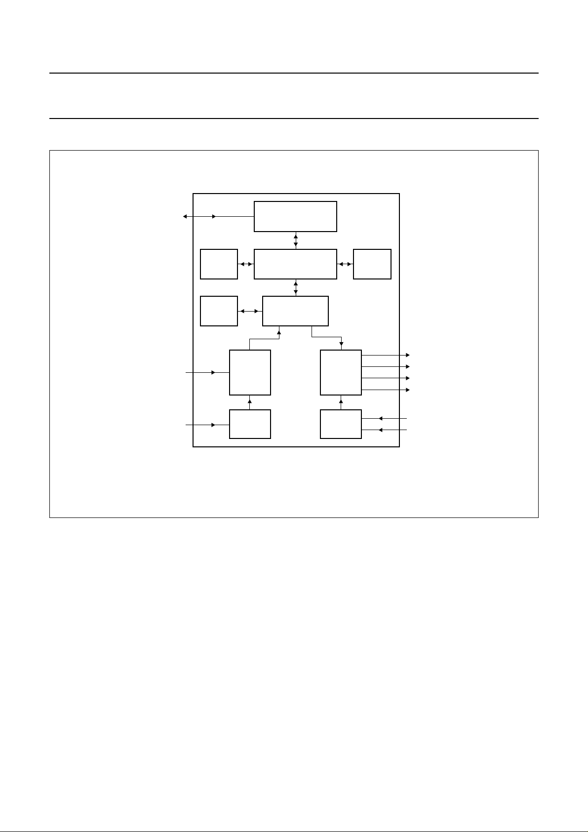
BLOCK DIAGRAM
handbook, full pagewidth
2
I
C-bus,
general I/O
TV CONTROL
AND
INTERFACE
CVBS
CVBS
ROM
DRAM
MICROCONTROLLER
(80C51)
MEMORY
INTERFACE
DATA
CAPTURE
DATA
CAPTURE
TIMING
Fig.1 Block diagram.
SAA5264
SAA5265
DISPLAY
DISPLAY
TIMING
SRAM
R
G
B
VDS
VSYNC
HSYNC
GSA018
1999 Oct 05 4
Page 5
Philips Semiconductors Preliminary specification
10 and 1 page intelligent teletext decoders SAA5264; SAA5265
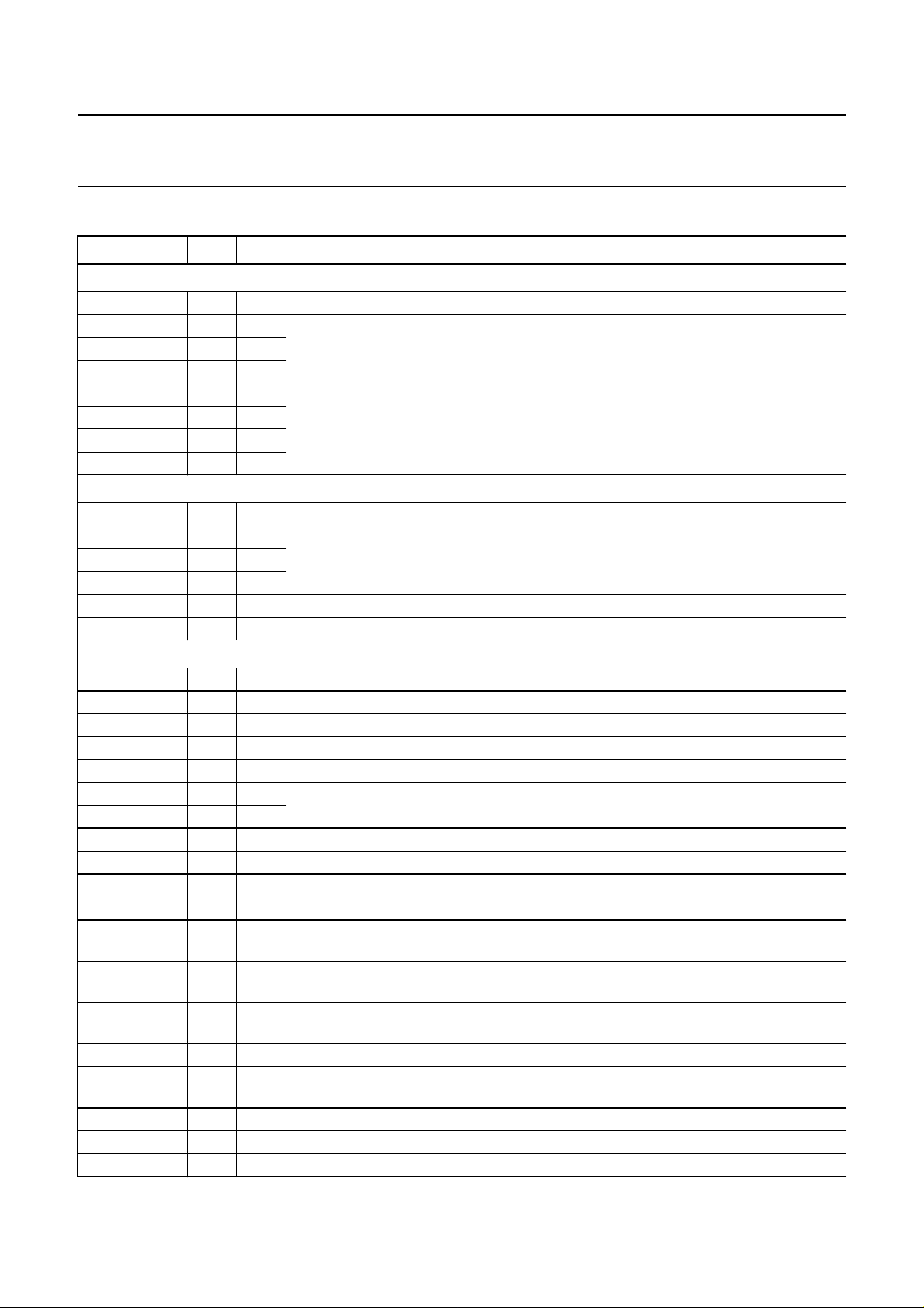
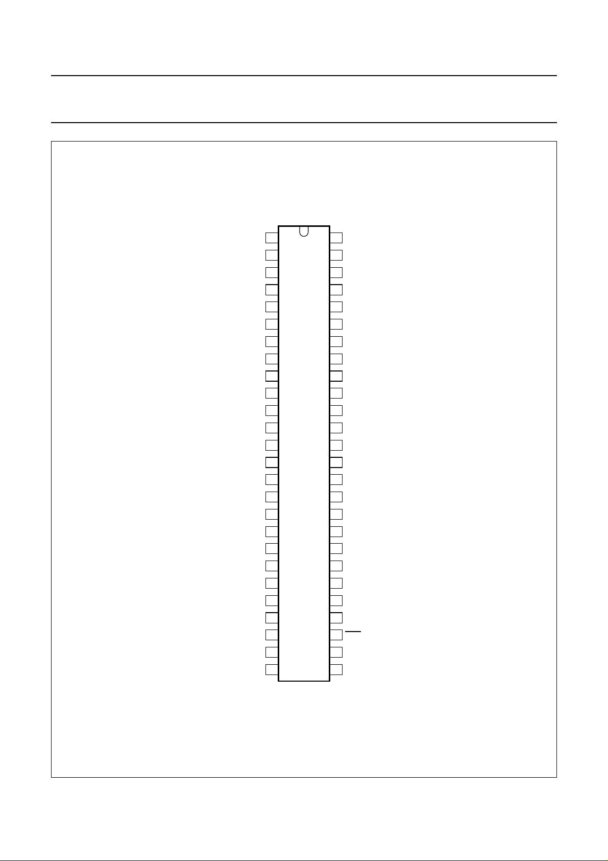
PINNING
SYMBOL PIN TYPE DESCRIPTION
Port 2: 8-bit programmable bidirectional port with alternative functions
P2.0/PWM 1 I/O output for 14-bit high precision Pulse Width Modulator (PWM)
P2.1/PWM0 2 I/O outputs for 6-bit PWMs 0 to 6
P2.2/PWM1 3 I/O
P2.3/PWM2 4 I/O
P2.4/PWM3 5 I/O
P2.5/PWM4 6 I/O
P2.6/PWM5 7 I/O
P2.7/PWM6 8 I/O
Port 3: 8-bit programmable bidirectional port with alternative functions
P3.0/ADC0 9 I/O inputs for the software Analog-to-Digital-Converter (ADC) facility
P3.1/ADC1 10 I/O
P3.2/ADC2 11 I/O
P3.3/ADC3 12 I/O
P3.4/PWM7 30 I/O output for 6-bit PWM7
V
SSC
Port 0: 8-bit programmable bidirectional port
SCL(NVRAM) 14 I I
SDA(NVRAM) 15 I/O I
P0.2 16 I/O input/output for general use
P0.3 17 I/O input/output for general use
P0.4 18 I/O input/output for general use
P0.5 19 I/O 8 mA current sinking capability for direct drive of Light Emitting Diodes (LEDs)
P0.6 20 I/O
P0.7 21 I/O input/output for general use
V
SSA
CVBS0 23 I Composite Video Baseband Signal (CVBS) input; a positive-going 1 V (peak-to-peak)
CVBS1 24 I
SYNC_FILTER 25 I sync-pulse-filter input for CVBS; this pin should be connected to V
IREF 26 I reference current input for analog circuits; for correct operation a 24 kΩ resistor
FRAME 27 O Frame de-interlace output synchronized with the VSYNC pulse to produce a
TEST 28 I not available; connect this pin to V
COR 29 O contrast reduction: open-drain, active LOW output which allows selective contrast
V
DDA
B 32 O Blue colour information pixel rate output
13 − core ground
2
C-bus Serial Clock input to Non-Volatile RAM
2
C-bus Serial Data input/output (Non-Volatile RAM)
22 − analog ground
input is required; connected via a 100 nF capacitor
100 nF capacitor
should be connected to V
SSA
non-interlaced display by adjustment of the vertical deflection circuits
reduction of the TV picture to enhance a mixed mode display
30 I/O P3.4/PWM7 (described above)
31 − analog supply voltage (3.3 V)
SSA
SSA
via a
1999 Oct 05 5
Page 6
Philips Semiconductors Preliminary specification
10 and 1 page intelligent teletext decoders SAA5264; SAA5265
SYMBOL PIN TYPE DESCRIPTION
G 33 O Green colour information pixel rate output
R 34 O Red colour information pixel rate output
VDS 35 O video/data switch push-pull output for pixel rate fast blanking
HSYNC 36 I horizontal sync pulse input: Schmitt triggered for a Transistor Transistor Level (TTL)
version; the polarity of this pulse is programmable by register bit TXT1.HPOLARITY
VSYNC 37 I vertical sync pulse input; Schmitt triggered for a TTL version; the polarity of this pulse
is programmable by register bit TXT1.V POLARITY
V
SSP
V
DDC
OSCGND 40 − crystal oscillator ground
XTALIN 41 I 12 MHz crystal oscillator input
XTALOUT 42 O 12 MHz crystal oscillator output
RESET 43 I reset input; if this pin is HIGH for at least 2 machine cycles (24 oscillator periods)
V
DDP
Port 1: 8-bit programmable bidirectional port
P1.0 45 I/O input/output for general use
P1.1 46 I/O input/output for general use
P1.2 47 I/O input/output for general use
P1.3 48 I/O input/output for general use
SCL 49 I I
SDA 50 I/O I
P1.4 51 I/O input/output for general use
P1.5 52 I/O input/output for general use
38 − periphery ground
39 − core supply voltage (+3.3 V)
while the oscillator is running, the device resets; this pin should be connected to V
via a capacitor
44 − periphery supply voltage (+3.3 V)
2
C-bus Serial Clock input from application
2
C-bus Serial Data input/output (application)
DDP
1999 Oct 05 6
Page 7
Philips Semiconductors Preliminary specification
10 and 1 page intelligent teletext decoders SAA5264; SAA5265
handbook, halfpage
P2.0/PWM
P2.1/PWM0
P2.2/PWM1
P2.3/PWM2
P2.4/PWM3
P2.5/PWM4
P2.6/PWM5
P2.7/PWM6
P3.0/ADC0
P3.1/ADC1
P3.2/ADC2
P3.3/ADC3
SCL(NVRAM)
SDA(NVRAM)
SYNC_FILTER
V
SSC
P0.2
P0.3
P0.4
P0.5
P0.6
P0.7
V
SSA
CVBS0
CVBS1
IREF
1
2
3
4
5
6
7
8
9
10
11
12
13
14
15
16
17
18
19
20
21
22
23
24
25
26
SAA5264
SAA5265
GSA016
52
P1.5
51
P1.4
50
SDA
49
SCL
48
P1.3
47
P1.2
46
P1.1
45
P1.0
44
V
43
RESET
42
XTALOUT
41
XTALIN
40
OSCGND
39
V
38
V
37
VSYNC
36
HSYNC
35
VDS
34
R
33
G
32
B
31
V
30
P3.4/PWM7
29
COR
28
TEST
27
FRAME
DDP
DDC
SSP
DDA
Fig.2 Pin configuration.
1999 Oct 05 7
Page 8
Philips Semiconductors Preliminary specification
10 and 1 page intelligent teletext decoders SAA5264; SAA5265
HIGH LEVEL COMMAND INTERFACE
The I2C-bus interface is used to pass control commands and data between the SAA5264/SAA5265 and the television
microcontroller. The interface uses high-level commands, which are backward compatible with the SAFARI.
The I2C-bus transmission formats are:
Table 1 User command
START I2C-BUS ADDRESS WRITE ACK COMMAND ACK STOP
Table 2 System command
2
START I
Table 3 User read
START I
CHARACTER SETS
C-BUS ADDRESS WRITE ACK COMMAND ACK PARAMETER ACK STOP
2
C-BUS ADDRESS READ ACK DATA ACK STOP
The following standard character sets are included in the SAA5264 and in the SAA5265:
Set 0 = Pan-European
Set 1 = Cyrillic
Set 2 = Greek/Turkish
Set 3 = French/Arabic
If you require any other character sets, please discuss them with your local Regional Sales Office first.
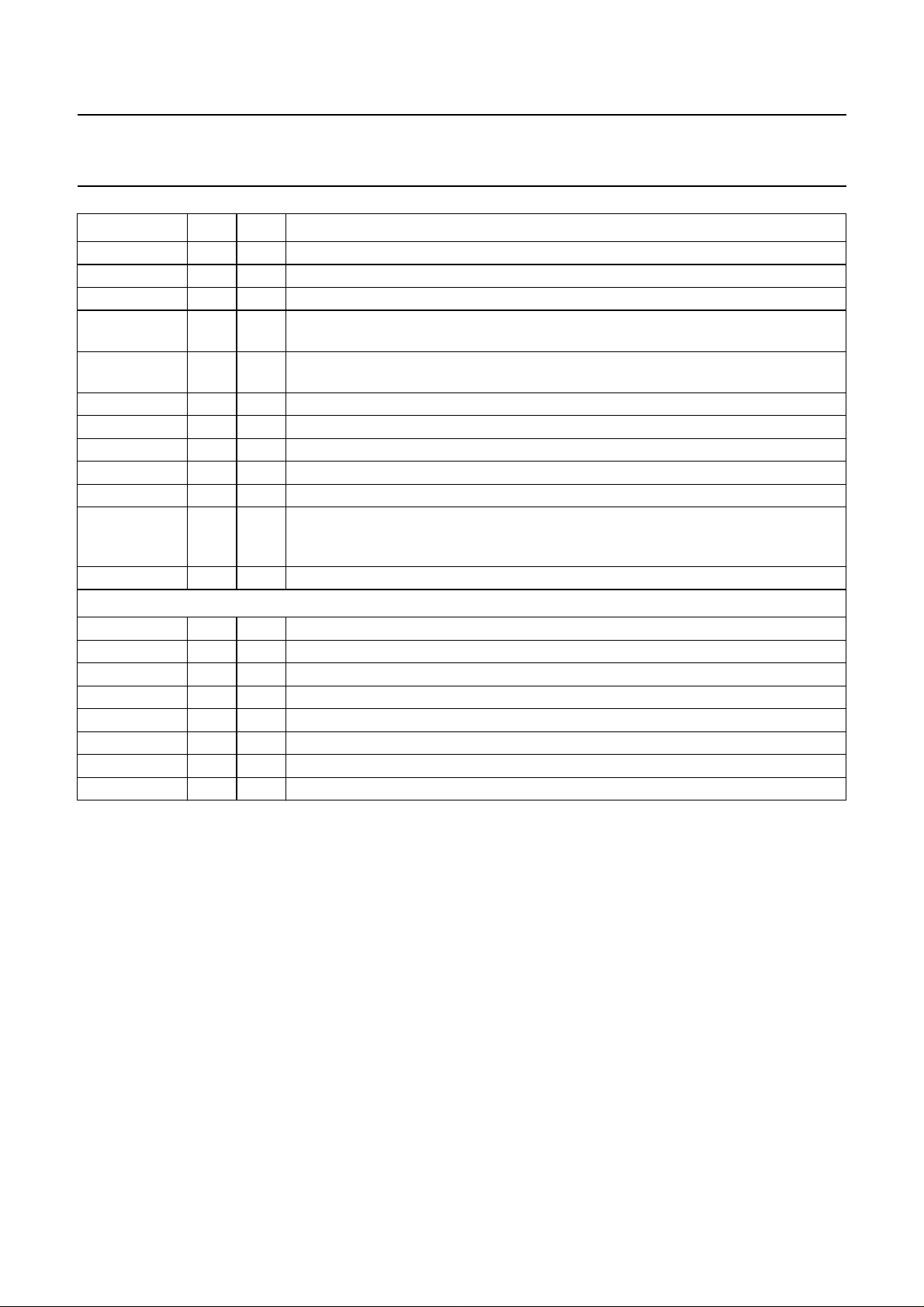
LIMITING VALUES
In accordance with Absolute Maximum Rating System (IEC 60134).
SYMBOL PARAMETER CONDITIONS MIN. MAX. UNIT
V
V
DDX
I
all supply voltages −0.5 +4.0 V
input voltage (any input) note 1 −0.5 VDD+0.5
V
or +4.1
V
I
O
I
IO(d)
T
T
O
amb
stg
output voltage (any output) note 1 −0.5 VDD+0.5 V
output current (each output) − 10 mA
diode DC input or output current − 20 mA
ambient temperature −20 +70 °C
storage temperature −55 +125 °C
Note
1. This maximum value refers to 5 V tolerant I/Os and may be 6 V maximum but only when V
is present.
DD
1999 Oct 05 8
Page 9

Philips Semiconductors Preliminary specification
10 and 1 page intelligent teletext decoders SAA5264; SAA5265
CHARACTERISTICS
VDD= 3.3 V ±10%; VSS=0V; T
SYMBOL PARAMETER CONDITIONS MIN. TYP. MAX. UNIT
Supplies
V
I
DDP
DDX
all supply voltages referenced to VSS3.0 3.3 3.6 V
periphery supply
current
I
DDC
I
DDC(idle)
core supply current normal mode − 15 18 mA
idle mode core supply
current
I
DDA
I
DDA(idle)
analog supply current − 45 48 mA
idle mode analog
supply current
Digital inputs
= −20 to +70 °C; unless otherwise specified.
amb
note 1 1 −− mA
− 4.6 6 mA
normal mode − 0.87 1 mA
RESET (
V
IL
PIN 43)
LOW-level input
voltage
V
IH
HIGH-level input
voltage
V
hys
Schmitt trigger input
hysteresis voltage
I
LI
R
pd(eq)
input leakage current VI=0 −− 0.17 µA
equivalent pull-down
resistance
HSYNC, VSYNC (PINS 36 AND 37)
V
IL
LOW-level input
voltage
V
IH
HIGH-level input
voltage
V
hys
Schmitt trigger input
hysteresis voltage
I
LI
Input leakage current VI=0toV
Digital outputs
FRAME, VDS (PINS 27 AND 35)
V
OL
LOW-level output
voltage
V
OH
HIGH-level output
voltage
t
o(r)
t
o(f)
output rise time between 10% and
output fall time between 10% and
−− 1.34 V
1.49 − 5.5 V
0.44 − 0.58 V
VI=V
DD
55.73 70.71 92.45 kΩ
−− 1.31 V
1.44 − 5.5 V
0.40 − 0.56 V
DD
−− 0.00 µA
IOL=3mA −− 0.13 V
IOH= 3 mA 2.84 −− V
7.50 8.85 10.90 ns
90%; CL=70pF
6.70 7.97 10.00 ns
90%; CL=70pF
1999 Oct 05 9
Page 10

Philips Semiconductors Preliminary specification
10 and 1 page intelligent teletext decoders SAA5264; SAA5265
SYMBOL PARAMETER CONDITIONS MIN. TYP. MAX. UNIT
COR (OPEN-DRAIN OUTPUT, PIN 29)
V
OL
LOW-level output
voltage
V
OH(pu)
HIGH-level pull-up
output voltage
V
IL
LOW-level input
voltage
V
IH
HIGH-level input
voltage
I
t
t
LI
o(r)
o(f)
input leakage current VI= 0 to V
output rise time between 10% and
output fall time between 10% and
Digital input/outputs
IOL=3mA −− 0.14 V
IOL= −3 mA;
2.84 −− V
push-pull
−− 0.00 V
0.00 − 5.50 V
DD
−− 0.12 µA
7.20 8.64 11.10 ns
90%; CL=70pF
4.90 7.34 9.40 ns
90%; CL=70pF
SCL(NVRAM), SDA(NVRAM), P0.4, P0.7, P1.0, P1.1, P2.1 TO P2.7, P3.0 TO P3.4
(PINS 14, 15, 18, 21, 45, 46, 2 TO 12, 30)
V
IL
LOW-level input
−− 1.28 V
voltage
V
IH
HIGH-level input
1.43 − 5.50 V
voltage
V
hys
Schmitt trigger input
0.41 − 0.55 V
hysteresis voltage
I
LI
V
OL
input leakage current VI= 0 to V
LOW-level output
IOL=4mA −− 0.18 V
DD
−− 0.01 µA
voltage
V
OH
t
o(r)
HIGH-level output
voltage
IOH= −4mA
push-pull
output rise time between 10% and
2.81 −− V
6.50 8.47 10.70 ns
90%; CL=70pF
push-pull
t
o(f)
output fall time between 10% and
5.70 7.56 10.00 ns
90%; CL=70pF
P1.2, P1.3, P2.0 (PINS 47, 48, 1)
V
IL
LOW-level input
−− 1.29 V
voltage
V
IH
HIGH-level input
1.45 − 5.50 V
voltage
V
hys
Schmitt trigger input
0.42 − 0.56 V
hysteresis voltage
I
LI
input leakage current VI= 0 to V
DD
−− 0.02 µA
1999 Oct 05 10
Page 11

Philips Semiconductors Preliminary specification
10 and 1 page intelligent teletext decoders SAA5264; SAA5265
SYMBOL PARAMETER CONDITIONS MIN. TYP. MAX. UNIT
V
OL
V
OH
t
o(r)
t
o(f)
P0.5, P0.6 (PINS 19, 20)
V
IL
V
IH
I
LI
V
hys
V
OL
V
OH
t
o(r)
t
o(f)
P1.4, P1.5 (OPEN-DRAIN)(PINS 51, 52)
V
IL
V
IH
V
hys
I
LI
V
OL
t
o(f)
Analog inputs
LOW-level output
IOL=4mA −− 0.17 V
voltage
HIGH-level output
voltage
IOH= −4mA
push-pull
output rise time between 10% and
90%; CL=70pF
push-pull
output fall time between 10% and
90%; CL=70pF
LOW-level input
voltage
HIGH-level input
voltage
input leakage current VI= 0 to V
DD
Schmitt trigger input
hysteresis voltage
LOW-level output
IOL=8mA −− 0.20 V
voltage
HIGH-level output
voltage
IOH= −8mA
push-pull
output rise time between 10% and
90%; CL=70pF
push-pull
output fall time between 10% and
90%; CL=70pF
LOW-level input
voltage
HIGH-level input
voltage
Schmitt trigger input
hysteresis voltage
input leakage current VI= 0 to V
LOW-level output
IOL=8mA −− 0.35 V
DD
voltage
output fall time between 10% and
90%; CL=70pF
2.81 −− V
7.00 8.47 10.50 ns
5.40 7.36 9.30 ns
−− 1.28 V
1.43 − 5.50 V
−− 0.11 µA
0.42 − 0.58 V
2.76 −− V
7.40 8.22 8.80 ns
4.20 4.57 5.20 ns
−− 1.45 V
1.62 − 5.5 V
0.49 − 0.60 V
−− 0.13 µA
69.70 83.67 103.30 ns
CVBS0 AND CVBS1(PINS 23 AND 24)
V
sync
sync voltage
0.1 0.3 0.6 V
amplitude
V
i(v)(p-p)
video input voltage
0.7 1.0 1.4 V
(peak-to-peak value)
1999 Oct 05 11
Page 12

Philips Semiconductors Preliminary specification
10 and 1 page intelligent teletext decoders SAA5264; SAA5265
SYMBOL PARAMETER CONDITIONS MIN. TYP. MAX. UNIT
Z
source
V
IH
C
i
IREF (PIN 26)
R
IREF
ADC0 TO ADC3 (PINS 9 TO 12)
V
IH
C
i
Analog outputs
B, G AND R(PINS 32 TO 34)
I
o(bl)
I
o(max)
I
o(70%max)
R
L
C
L
Analog input/output
source impedance 0 − 250 Ω
HIGH-level input
3.0 − V
+0.3 V
DDA
voltage
input capacitance −− 10 pF
resistance from IREF
to V
SSA
HIGH-level input
resistor
tolerance = 2%
− 24 − kΩ
−− V
DDA
V
voltage
input capacitance −− 10 pF
output current
V
= 3.3 V −10 − +10 µA
DDA
(black level)
output current
(maximum intensity)
V
= 3.3 V
DDA
intensity level
6.0 6.67 7.3 mA
code = 15 (Dec)
output current
(70% of maximum
intensity)
load resistance (to
V
)
SSA
V
= 3.3 V
DDA
intensity level
code = 0 (Dec)
resistor
tolerance = 5%
4.2 4.7 5.1 mA
− 150 −Ω
load capacitance −− 15 pF
SYNC_FILTER (PIN 25)
C
stg
V
sync(nom)
storage capacitor
(to V
SSA
)
sync filter level
− 100 − nF
0.35 0.55 0.75 V
voltage with nominal
sync amplitude
Crystal oscillator
XTALIN (PIN 41)
V
IL
LOW-level input
V
SSA
voltage
V
IH
HIGH-level input
−− V
voltage
C
i
input capacitance −− 10 pF
1999 Oct 05 12
−− V
DDA
V
Page 13

Philips Semiconductors Preliminary specification
10 and 1 page intelligent teletext decoders SAA5264; SAA5265
SYMBOL PARAMETER CONDITIONS MIN. TYP. MAX. UNIT
XTALOUT (PIN 42)
C
o
Crystal specification; notes 2 and 3
f
xtal(nom)
C
L
C
mot
R
xtal
C
osc
C
xtal(hold)
T
xtal
X
j
X
d
Notes
1. Periphery supply current is dependent on I/O external components and voltage levels.
2. Crystal order number 4322 143 05561. If crystal 4322 143 05561 is not used, then the formulae in the crystal
specification should be used.
3. C
chip at XTALIN and at XTALOUT. C
at XTALIN and XTALOUT. The maximum value for C
output capacitance −− 10 pF
nominal frequency fundamental
− 12 − MHz
mode
load capacitance −− 30 pF
motional capacitance T
crystal resonance
=25°C −− 20 fF
amb
T
=25°C −− 60 Ω
amb
resistance
capacitance at
T
=25°C −−pF
amb
2CLC
– C
chip
–
stray
XTALIN, XTALOUT
C
crystal holder
capacitance
crystal temperature
T
=25°C −− pF
amb
35
–
−20 +25 +85 °C
osc
----------- 2
–
C
-------------
range
adjustment tolerance T
=25°C −− ±50 × 10
amb
drift −− ±100 × 10
may need to be reduced from the initially selected value. C
osc
is a value for the mean of the stray capacitances due to the external circuit
stray
xtal(hold)
= 7 pF, the mean of the capacitances due to the
chip
is to ensure start-up.
−6
−6
chip
2
C
–
---------------
stray
2
1999 Oct 05 13
Page 14

Philips Semiconductors Preliminary specification
10 and 1 page intelligent teletext decoders SAA5264; SAA5265
I2C-BUS CHARACTERISTICS
SYMBOL PARAMETER
FAST-MODE I2C-bus
MIN. MAX.
f
SCL
t
BUF
t
HD;STA
SCL clock frequency 0 400 kHz
bus free time between a STOP and START condition 1.3 −µs
hold time START condition; after this period, the first clock
0.6 −µs
pulse is generated
t
LOW
t
HIGH
t
SU;STA
t
HD;DAT
t
SU;DAT
t
r
t
f
t
SU;STO
C
b
SCL LOW time 1.3 −µs
SCL HIGH time 0.6 −µs
set-up time repeated START 0.6 −µs
data hold time; notes 1 and 2 0 0.9 µs
data set-up time; note 3 100 − ns
rise time SDA and SCL; note 4 20 300 ns
fall time SDA and SCL; note 4 20 300 ns
set-up time STOP condition 0.6 −µs
capacitive load of each bus line − 400 pF
Notes
1. A device must internally provide a hold time of at least 300 ns for the SDA signal (referenced to the V
SCL signal) in order to bridge the undefined region of the falling edge of SCL.
2. The maximum t
3. A fast-mode I2C-bus device can be used in a standard-mode I2C-bus system, but the requirement t
must then be met. This will automatically be the case if the device does not stretch t
stretch t
LOW(SCL)
has only to be met if the device does not stretch the LOW period of the SCL signal (t
HD;DAT
LOW(SCL)
, it must output the next data bit to the SDA line t
r(max)+tSU;DAT
= 1000 + 250 = 1250 ns (according
SU;DAT
. If such a device does
to the standard-mode I2C-bus specification) before the SCL line is released.
4. Cb= total capacitance of one bus line in pF.
IHmin
UNIT
of the
LOW(SCL)
≥250 ns
).
1999 Oct 05 14
Page 15

Philips Semiconductors Preliminary specification
10 and 1 page intelligent teletext decoders SAA5264; SAA5265
EMC GUIDELINES
Optimization of circuit return paths and minimization of
commonmode emission will be assisted byusinga double
sided Printed Circuit Board (PCB) with low inductance
ground plane.
On a single-sided PCB a local ground plane under the
whole IC should be presentas shown in Fig.3. This should
have the widest possible connection between the PCB
ground and bulk electrolytic decoupling capacitor.
Preferably, the PCB local ground plane connection should
not be connected to other grounds on route to the PCB
ground. Do not use wire links. Wire links cause ground
inductance which increases ground bounce.
The supply pins can be decoupled at the ground pin plane
below the IC. This is easily achieved by using surface
mount capacitors, which, at high frequency, are more
effective than components with leads.
Using a device socket would increase the area and
therefore increase the inductance of the external bypass
loop.
To provide a high-impedance to any high frequency
signals on the VDD supplies to the IC, a ferrite bead or
inductor can be connected in series with the supply line
close to the decoupling capacitor. To prevent signal
radiation, pull-up resistors of signal outputs should not be
connected to the VDD supply on the IC side of the ferrite
bead or inductor.
OSCGND should only be connected to the crystal load
capacitors and not to any other ground connection.
Distances to physical connections of associated active
devices should be as short as possible.
PCB output tracks should have close proximity, mutually
coupled, ground return paths.
handbook, full pagewidth
under-IC GND plane
GND connection
note: no wire links
other
GND
connections
GND
+3.3 V
electrolytic decoupling capacitor (2 µF)
SSP
DDP
V
DDC
V
V
V
SSC
V
ferrite beads
SM decoupling capacitors (10 to 100 nF)
DDA
V
under-IC GND plane
SSA
IC
MBK979
Fig.3 Power supply connections for EMC.
1999 Oct 05 15
Page 16

Philips Semiconductors Preliminary specification
10 and 1 page intelligent teletext decoders SAA5264; SAA5265
QUALITY AND RELIABILITY
This device will meet Philips Semiconductors general quality specification for business group
Circuits SNW-FQ-611-Part E”
. The principal requirements are shown in Tables 4 to 7.
Group A
Table 4 Acceptance tests per lot; note 1
TEST REQUIREMENTS
Mechanical cumulative target: <80 ppm
Electrical cumulative target: <100 ppm
Note
1. ppm = fraction of defective devices, in parts per million.
Group B
Table 5 Processability tests (by package family)
TEST REQUIREMENTS
Solderability 0/16 on all lots
Mechanical 0/15 on all lots
Solder heat resistance 0/15 on all lots
Group C
Table 6 Reliability tests (by package family); note1
“Consumer Integrated
TEST CONDITIONS REQUIREMENTS
Operational life 168 hours at T
Humidity life temperature, humidity, bias 1000 hours;
=85°C, 85% RH (or equivalent test)
T
amb
Temperature cycling performance T
stg(min)
to T
= 150 °C <1000 FPM at Tj= 150 °C
j
<2000 FPM
stg(max)
<2000 FPM
Note
1. FPM = fraction of devices failing at test condition, in Failures Per Million.
Table 7 Reliability tests (by device type)
TEST CONDITIONS REQUIREMENTS
ESD and latch-up ESD Human body model 100 pF, 1.5 kΩ 2000 V
ESD Machine model 200 pF, 0 Ω 200 V
latch-up 100 mA, 1.5 × V
(absolute maximum)
DD
1999 Oct 05 16
Page 17

This text is here in white to force landscape pages to be rotated correctly when browsing through the pdf in the Acrobat reader.This text is here in
_white to force landscape pages to be rotated correctly when browsing through the pdf in the Acrobat reader.This text is here inThis text is here in
white to force landscape pages to be rotated correctly when browsing through the pdf in the Acrobat reader. white to force landscape pages to be ...
1999 Oct 05 17
handbook, full pagewidth
APPLICATION INFORMATION
Philips Semiconductors Preliminary specification
10 and 1 page intelligent teletext decoders SAA5264; SAA5265
A0
A1
A2
V
SS
EEPROM
PCF8582E
user ports
V
V
DD
RC
SCL
SDA
DD
V
DD
P2.0/PWM
P2.1/PWM0
P2.2/PWM1
P2.3/PWM2
P2.4/PWM3
P2.5/PWM4
P2.6/PWM5
P2.7/PWM6
P3.0/ADC0
P3.1/ADC1
P3.2/ADC2
P3.3/ADC3
SCL(NVRAM)
SDA(NVRAM)
V
DD
1 kΩ
1 kΩ
CVBS
CVBS
100 nF
100 nF
100 nF
SYNC_FILTER
24 kΩ
V
SSC
P0.2
P0.3
P0.4
P0.5
P0.6
P0.7
V
SSA
CVBS0
CVBS1
IREF
1
2
3
4
5
6
7
8
9
10
11
12
13
14
15
16
17
18
19
20
21
22
23
24
25
26
SAA5264
SAA5265
P1.5
52
P1.4
51
SDA
50
SCL
49
P1.3
48
P1.2
47
P1.1
46
P1.0
45
V
44
RESET
43
XTALOUT
42
XTALIN
41
OSCGND
40
V
39
V
38
VSYNC
37
HSYNC
36
VDS
35
R
34
G
33
B
32
V
31
P3.4/PWM7
30
COR
29
TEST
28
FRAME
27
DDP
DDC
SSP
DDA
V
DD
12 MHz
V
DD
V
DD
10 µF
V
DD
56 pF
field flyback
line flyback
V
150
DD
SDA
SCL
V
DD
100
nF
Ω
GSA035
47
µF
V
DD
Bi-directional ports have been configured as open-drain. Output ports have been configured as push-pull.
Fig.4 Application diagram.
Page 18

Philips Semiconductors Preliminary specification
10 and 1 page intelligent teletext decoders SAA5264; SAA5265
PACKAGE OUTLINE
SDIP52: plastic shrink dual in-line package; 52 leads (600 mil)
SOT247-1
seating plane
L
Z
52
1
pin 1 index
D
A
2
A
A
1
e
b
w M
b
1
27
E
26
c
M
(e )
M
E
1
H
0 5 10 mm
scale
DIMENSIONS (mm are the original dimensions)
A
A
A
UNIT b
Note
1. Plastic or metal protrusions of 0.25 mm maximum per side are not included.
mm
OUTLINE
VERSION
SOT247-1
max.
5.08 0.51 4.0
12
min.
max.
IEC JEDEC EIAJ
1.3
0.8
b
1
0.53
0.40
REFERENCES
0.32
0.23
cEe M
(1) (1)
D
47.9
47.1
1999 Oct 05 18
14.0
13.7
1
L
M
E
3.2
15.80
2.8
15.24
EUROPEAN
PROJECTION
17.15
15.90
e
w
H
0.181.778 15.24
ISSUE DATE
90-01-22
95-03-11
max.
1.73
(1)
Z
Page 19

Philips Semiconductors Preliminary specification
10 and 1 page intelligent teletext decoders SAA5264; SAA5265
SOLDERING
Introduction to soldering through-hole mount
packages
This text gives a brief insight to wave, dip and manual
soldering.Amore in-depth account of soldering ICs can be
found in our
Packages”
Wave soldering is the preferred method for mounting of
through-hole mount IC packages on a printed-circuit
board.
Soldering by dipping or by solder wave
The maximum permissible temperature of the solder is
260 °C; solder at this temperature must not be in contact
with the joints for more than 5 seconds.
Suitability of through-hole mount IC packages for dipping and wave soldering methods
DBS, DIP, HDIP, SDIP, SIL suitable suitable
Note
1. For SDIP packages, the longitudinal axis must be parallel to the transport direction of the printed-circuit board.
“Data Handbook IC26; Integrated Circuit
(document order number 9398 652 90011).
PACKAGE
Thetotalcontacttimeofsuccessivesolderwavesmustnot
exceed 5 seconds.
The device may be mounted up to the seating plane, but
the temperature of the plastic body must not exceed the
specified maximum storage temperature (T
printed-circuit board has been pre-heated, forced cooling
may be necessary immediately after soldering to keep the
temperature within the permissible limit.
Manual soldering
Apply the soldering iron (24 V or less) to the lead(s) of the
package, either below the seating plane or not more than
2 mm above it. If the temperature of the soldering iron bit
is less than 300 °C it may remain in contact for up to
10 seconds. If the bit temperature is between
300 and 400 °C, contact may be up to 5 seconds.
SOLDERING METHOD
DIPPING WAVE
(1)
stg(max)
). If the
1999 Oct 05 19
Page 20

Philips Semiconductors Preliminary specification
10 and 1 page intelligent teletext decoders SAA5264; SAA5265
DEFINITIONS
Data sheet status
Objective specification This data sheet contains target or goal specifications for product development.
Preliminary specification This data sheet contains preliminary data; supplementary data may be published later.
Product specification This data sheet contains final product specifications.
Limiting values
Limiting values given are in accordance with the Absolute Maximum Rating System (IEC 134). Stress above one or
more of the limiting values may cause permanent damage to the device. These are stress ratings only and operation
of the device at these or at any other conditions above those given in the Characteristics sections of the specification
is not implied. Exposure to limiting values for extended periods may affect device reliability.
Application information
Where application information is given, it is advisory and does not form part of the specification.
LIFE SUPPORT APPLICATIONS
These products are not designed for use in life support appliances, devices, or systems where malfunction of these
products can reasonably be expected to result in personal injury. Philips customers using or selling these products for
use in such applications do so at their own risk and agree to fully indemnify Philips for any damages resulting from such
improper use or sale.
PURCHASE OF PHILIPS I
2
C COMPONENTS
2
Purchase of Philips I
components in the I2C system provided the system conforms to the I2C specification defined by
Philips. This specification can be ordered using the code 9398 393 40011.
C components conveys a license under the Philips’ I2C patent to use the
1999 Oct 05 20
Page 21

Philips Semiconductors Preliminary specification
10 and 1 page intelligent teletext decoders SAA5264; SAA5265
NOTES
1999 Oct 05 21
Page 22

Philips Semiconductors Preliminary specification
10 and 1 page intelligent teletext decoders SAA5264; SAA5265
NOTES
1999 Oct 05 22
Page 23

Philips Semiconductors Preliminary specification
10 and 1 page intelligent teletext decoders SAA5264; SAA5265
NOTES
1999 Oct 05 23
Page 24

Philips Semiconductors – a w orldwide compan y
Argentina: see South America
Australia: 3 Figtree Drive, HOMEBUSH, NSW 2140,
Tel. +61 2 9704 8141, Fax. +61 2 9704 8139
Austria: Computerstr. 6, A-1101 WIEN, P.O. Box 213,
Tel. +43 1 60 101 1248, Fax. +43 1 60 101 1210
Belarus: Hotel Minsk Business Center, Bld. 3, r. 1211, Volodarski Str. 6,
220050 MINSK, Tel. +375 172 20 0733, Fax. +375 172 20 0773
Belgium: see The Netherlands
Brazil: see South America
Bulgaria: Philips Bulgaria Ltd., Energoproject, 15th floor,
51 James Bourchier Blvd., 1407 SOFIA,
Tel. +359 2 68 9211, Fax. +359 2 68 9102
Canada: PHILIPS SEMICONDUCTORS/COMPONENTS,
Tel. +1 800 234 7381, Fax. +1 800 943 0087
China/Hong Kong: 501 Hong Kong Industrial Technology Centre,
72 Tat Chee Avenue, Kowloon Tong, HONG KONG,
Tel. +852 2319 7888, Fax. +852 2319 7700
Colombia: see South America
Czech Republic: see Austria
Denmark: Sydhavnsgade 23, 1780 COPENHAGEN V,
Tel. +45 33 29 3333, Fax. +45 33 29 3905
Finland: Sinikalliontie 3, FIN-02630 ESPOO,
Tel. +358 9 615 800, Fax. +358 9 6158 0920
France: 51 Rue Carnot, BP317, 92156 SURESNES Cedex,
Tel. +33 1 4099 6161, Fax. +33 1 4099 6427
Germany: Hammerbrookstraße 69, D-20097 HAMBURG,
Tel. +49 40 2353 60, Fax. +49 40 2353 6300
Hungary: see Austria
India: Philips INDIA Ltd, Band Box Building, 2nd floor,
254-D, Dr. Annie Besant Road, Worli, MUMBAI 400 025,
Tel. +91 22 493 8541, Fax. +91 22 493 0966
Indonesia: PTPhilips DevelopmentCorporation,Semiconductors Division,
Gedung Philips, Jl. Buncit Raya Kav.99-100, JAKARTA 12510,
Tel. +62 21 794 0040 ext. 2501, Fax. +62 21 794 0080
Ireland: Newstead, Clonskeagh, DUBLIN 14,
Tel. +353 1 7640 000, Fax. +353 1 7640 200
Israel: RAPAC Electronics, 7 Kehilat Saloniki St, PO Box 18053,
TEL AVIV 61180, Tel. +972 3 645 0444, Fax. +972 3 649 1007
Italy: PHILIPS SEMICONDUCTORS, ViaCasati,23 - 20052 MONZA (MI),
Tel. +39 039 203 6838, Fax +39 039 203 6800
Japan: Philips Bldg 13-37, Kohnan 2-chome, Minato-ku,
TOKYO 108-8507, Tel. +81 3 3740 5130, Fax. +81 3 3740 5057
Korea: Philips House, 260-199 Itaewon-dong, Yongsan-ku, SEOUL,
Tel. +82 2 709 1412, Fax. +82 2 709 1415
Malaysia: No. 76 Jalan Universiti, 46200 PETALING JAYA, SELANGOR,
Tel. +60 3 750 5214, Fax. +60 3 757 4880
Mexico: 5900 Gateway East, Suite 200, EL PASO, TEXAS 79905,
Tel. +9-5 800 234 7381, Fax +9-5 800 943 0087
Middle East: see Italy
Netherlands: Postbus 90050, 5600 PB EINDHOVEN, Bldg. VB,
Tel. +31 40 27 82785, Fax. +31 40 27 88399
New Zealand: 2 Wagener Place, C.P.O. Box 1041, AUCKLAND,
Tel. +64 9 849 4160, Fax. +64 9 849 7811
Norway: Box 1, Manglerud 0612, OSLO,
Tel. +47 22 74 8000, Fax. +47 22 74 8341
Pakistan: see Singapore
Philippines: Philips Semiconductors Philippines Inc.,
106 Valero St. Salcedo Village, P.O. Box 2108 MCC, MAKATI,
Metro MANILA, Tel. +63 2 816 6380, Fax. +63 2 817 3474
Poland: Al.Jerozolimskie 195 B, 02-222 WARSAW,
Tel. +48 22 5710 000, Fax. +48 22 5710 001
Portugal: see Spain
Romania: see Italy
Russia: Philips Russia, Ul. Usatcheva 35A, 119048 MOSCOW,
Tel. +7 095 755 6918, Fax. +7 095 755 6919
Singapore: Lorong 1, Toa Payoh, SINGAPORE 319762,
Tel. +65 350 2538, Fax. +65 251 6500
Slovakia: see Austria
Slovenia: see Italy
South Africa: S.A. PHILIPS Pty Ltd., 195-215 Main Road Martindale,
2092 JOHANNESBURG, P.O. Box 58088 Newville 2114,
Tel. +27 11 471 5401, Fax. +27 11 471 5398
South America: Al. Vicente Pinzon, 173, 6th floor,
04547-130 SÃO PAULO, SP, Brazil,
Tel. +55 11 821 2333, Fax. +55 11 821 2382
Spain: Balmes 22, 08007 BARCELONA,
Tel. +34 93 301 6312, Fax. +34 93 301 4107
Sweden: Kottbygatan 7, Akalla, S-16485 STOCKHOLM,
Tel. +46 8 5985 2000, Fax. +46 8 5985 2745
Switzerland: Allmendstrasse 140, CH-8027 ZÜRICH,
Tel. +41 1 488 2741 Fax. +41 1 488 3263
Taiwan: Philips Semiconductors, 6F, No. 96, Chien Kuo N. Rd., Sec. 1,
TAIPEI, Taiwan Tel. +886 2 2134 2886, Fax. +886 2 2134 2874
Thailand: PHILIPS ELECTRONICS (THAILAND) Ltd.,
209/2 Sanpavuth-Bangna Road Prakanong, BANGKOK 10260,
Tel. +66 2 745 4090, Fax. +66 2 398 0793
Turkey: Yukari Dudullu, Org. San. Blg., 2.Cad. Nr. 28 81260 Umraniye,
ISTANBUL, Tel. +90 216 522 1500, Fax. +90 216 522 1813
Ukraine: PHILIPS UKRAINE, 4 Patrice Lumumba str., Building B, Floor 7,
252042 KIEV, Tel. +380 44 264 2776, Fax. +380 44 268 0461
United Kingdom: Philips Semiconductors Ltd., 276 Bath Road, Hayes,
MIDDLESEX UB3 5BX, Tel. +44 208 730 5000, Fax. +44 208 754 8421
United States: 811 East Arques Avenue, SUNNYVALE, CA 94088-3409,
Tel. +1 800 234 7381, Fax. +1 800 943 0087
Uruguay: see South America
Vietnam: see Singapore
Yugoslavia: PHILIPS, Trg N. Pasica 5/v, 11000 BEOGRAD,
Tel. +381 11 62 5344, Fax.+381 11 63 5777
For all other countries apply to: Philips Semiconductors,
International Marketing & Sales Communications, Building BE-p, P.O. Box 218,
5600 MD EINDHOVEN, The Netherlands, Fax. +31 40 27 24825
© Philips Electronics N.V. SCA
All rights are reserved. Reproduction in whole or in part is prohibited without the prior written consent of the copyright owner.
The information presented in this document does not form part of any quotation or contract, is believed to be accurate and reliable and may be changed
without notice. No liability will be accepted by the publisher for any consequence of its use. Publication thereof does not convey nor imply any license
under patent- or other industrial or intellectual property rights.
1999
Internet: http://www.semiconductors.philips.com
68
Printed in The Netherlands 545004/01/pp24 Date of release:1999 Oct 05 Document order number: 9397 750 06113
 Loading...