

Page 1

INTEGRATED CIRCUITS
DATA SH EET
SAA4990H
Progressive scan-Zoom and Noise
reduction IC (PROZONIC)
Preliminary specification
File under Integrated Circuits, IC02
1996 Oct 25
Page 2

Philips Semiconductors Preliminary specification
Progressive scan-Zoom and Noise
SAA4990H
reduction IC (PROZONIC)
FEATURES
• Progressive scan conversion
(262.5 to 525 or 312.5 to 625 lines/field)
• Field rate up-conversion (50 to 100 Hz or 60 to 120 Hz)
• Line flicker reduction
• Noise and cross-colour reduction
• Variable vertical sample rate conversion
• Movie phase detection
• Synchronous No parity Eight bit Reception and
Transmission (SNERT) interface.
QUICK REFERENCE DATA
SYMBOL PARAMETER MIN. MAX. UNIT
V
T
DDD
amb
digital supply voltage 4.5 5.5 V
operating ambient temperature 0 70 °C
GENERAL DESCRIPTION
The Progressive scan-Zoom and Noise reduction IC,
abbreviated as PROZONIC, is designed for applications
together with:
SAA4951WP Economy Controller (ECO3)
SAA4952H (memory controller)
SAA7158WP Back END IC (BENDIC)
SAA4995WP PANorama IC (PANIC)
SAA4970T ECOnomical video processing Back END IC
(ECOBENDIC)
TMS4C2970/71 (serial field memories)
TDA8755/8753A (A/D converter 4 : 1 : 1 format)
83C652/54 type of microcontroller.
ORDERING INFORMATION
TYPE
NUMBER
SAA4990H QFP80 plastic quad flat package; 80 leads (lead length 1.95 mm); body 14 × 20 × 2.8 mm SOT318-2
NAME DESCRIPTION VERSION
PACKAGE
1996 Oct 25 2
Page 3
Philips Semiconductors Preliminary specification
Progressive scan-Zoom and Noise
reduction IC (PROZONIC)
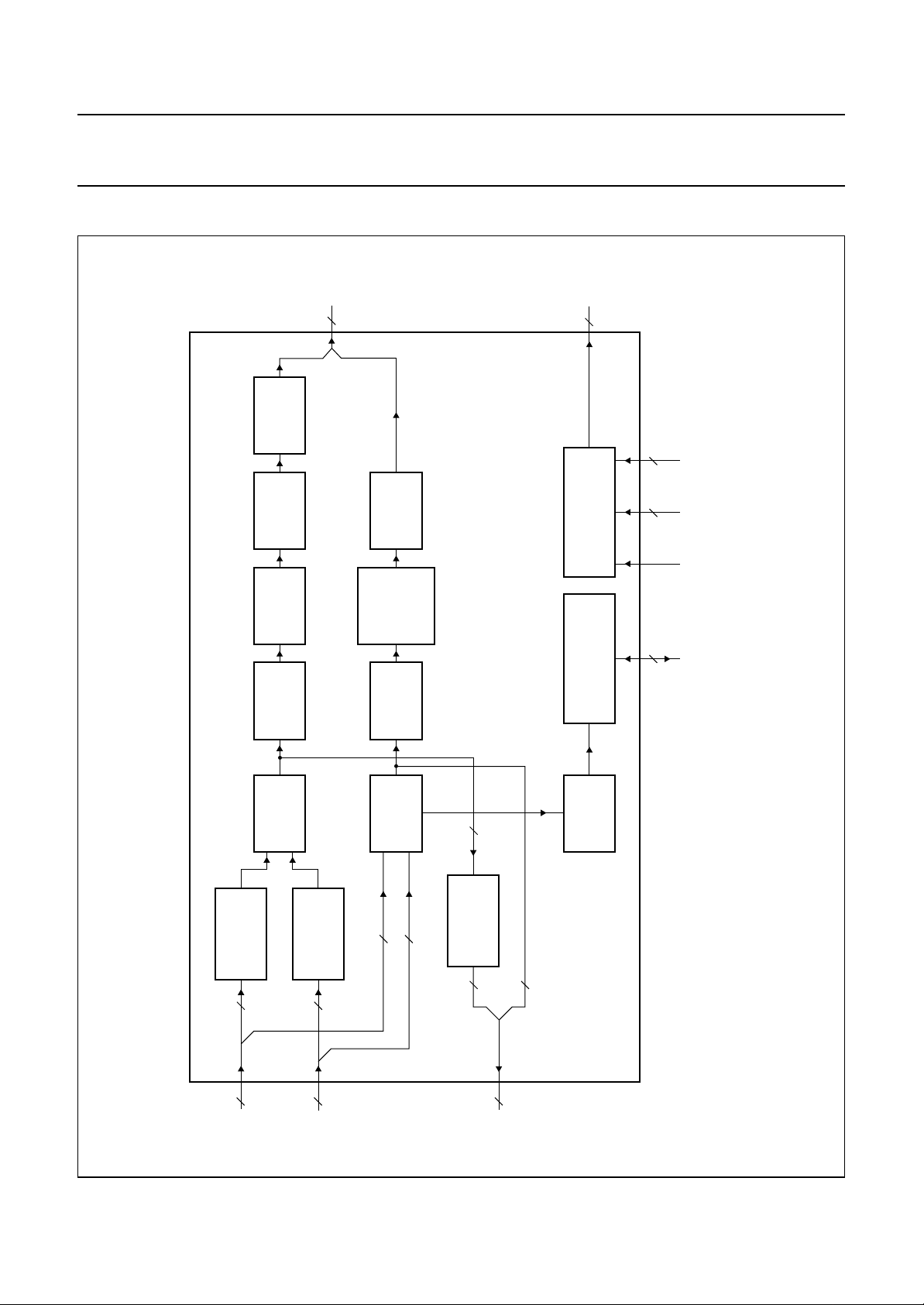
BLOCK DIAGRAM
D
YUV
12
FORMATTER
LINE
MIXER
MEMORY 3
LINE
MIXER
MEMORY 3
SAA4990H
RE1
RE2
WE2
3
CONTROL BLOCK
MGE024
SAA4990H
CK RE, WEVD, HD
book, full pagewidth
LINE
MIXER
MEMORY 2
LINE
MEMORY 1
NOISE
REDUCTION
REFORMATTER
4
UV1
REFORMATTER
4
UV2
LINE
MEDIAN
MEMORY 2
LINE
MEMORY 1
NOISE
REDUCTION
8
8
Y1
Y2
FILTER
84
FORMATTER
3 2 2
(SNERT)
INTERFACE
MICROPROCESSOR
SNRST
SNCL, SNDA,
Fig.1 Block diagram.
MOVIE
PHASE
DETECTOR
8
12
A
YUV
12
B
YUV
1996 Oct 25 3
12
C
YUV
Page 4

Philips Semiconductors Preliminary specification
Progressive scan-Zoom and Noise
reduction IC (PROZONIC)
PINNING
SYMBOL PIN TYPE DESCRIPTION
TEST1/AP 1 input action pin for testing, to be connected to V
TEST2/SP 2 input shift pin for testing, to be connected to V
RE1 3 output read enable to FM1
V
SS1
V
DD1
YUV
C7
YUV
C6
YUV
C5
YUV
C4
YUV
C3
V
SS2
V
DD2
YUV
C2
YUV
C1
YUV
C0
YUV
C11
YUV
C10
YUV
C9
YUV
C8
CK 20 input master clock, nominal 27 or 32 MHz
V
SS3
V
DD3
WE2 23 output write enable to FM2
RE2 24 output read enable to FM2
YUV
B8
YUV
B9
YUV
B10
YUV
B11
YUV
B0
YUV
B1
YUV
B2
YUV
B3
V
DD4
V
SS4
YUV
B4
YUV
B5
YUV
B6
YUV
B7
RE 39 input master read enable
VD 40 input field frequent reset, vertical display
4 ground ground 1
5 supply supply voltage 1
6 output Y bit 7 to FM2
7 output Y bit 6 to FM2
8 output Y bit 5 to FM2
9 output Y bit 4 to FM2
10 output Y bit 3 to FM2
11 ground ground 2
12 supply supply voltage 2
13 output Y bit 2 to FM2
14 output Y bit 1 to FM2
15 output Y bit 0 to FM2
16 output UV bit 3 to FM2
17 output UV bit 2 to FM2
18 output UV bit 1 to FM2
19 output UV bit 0 to FM2
21 ground ground 3
22 supply supply voltage 3
25 input UV bit 0 from FM2
26 input UV bit 1 from FM2
27 input UV bit 2 from FM2
28 input UV bit 3 from FM2
29 input Y bit 0 from FM2
30 input Y bit 1 from FM2
31 input Y bit 2 from FM2
32 input Y bit 3 from FM2
33 supply supply voltage 4
34 ground ground 4
35 input Y bit 4 from FM2
36 input Y bit 5 from FM2
37 input Y bit 6 from FM2
38 input Y bit 7 from FM2
SAA4990H
SS
SS
1996 Oct 25 4
Page 5

Philips Semiconductors Preliminary specification
Progressive scan-Zoom and Noise
SAA4990H
reduction IC (PROZONIC)
SYMBOL PIN TYPE DESCRIPTION
HD 41 input horizontal reference signal
YUV
D8
YUV
D9
YUV
D10
V
DD5
V
SS5
YUV
D11
YUV
D0
YUV
D1
YUV
D2
V
DD6
V
SS6
YUV
D3
YUV
D4
YUV
D5
YUV
D6
YUV
D7
V
DD7
V
SS7
SNRST 60 input field frequent reset from microcontroller; reset for SNERT interface
SNDA 61 I/O data for SNERT interface
SNCL 62 input clock for SNERT interface
AUX 63 output spare output from line-sequencer
H
O
n.c. 65 − not connected
n.c. 66 − not connected
YUV
A7
YUV
A6
YUV
A5
YUV
A4
YUV
A3
YUV
A2
V
SS8
V
DD8
YUV
A1
YUV
A0
YUV
A11
YUV
A10
YUV
A9
YUV
A8
42 output UV bit 0
43 output UV bit 1
44 output UV bit 2
45 supply supply voltage 5
46 ground ground 5
47 output UV bit 3
48 output Y bit 0
49 output Y bit 1
50 output Y bit 2
51 supply supply voltage 6
52 ground ground 6
53 output Y bit 3
54 output Y bit 4
55 output Y bit 5
56 output Y bit 6
57 output Y bit 7
58 supply supply voltage 7
59 ground ground 7
64 output output hold to e.g. LC display
67 input Y bit 7 from FM1
68 input Y bit 6 from FM1
69 input Y bit 5 from FM1
70 input Y bit 4 from FM1
71 input Y bit 3 from FM1
72 input Y bit 2 from FM1
73 ground ground 8
74 supply supply voltage 8
75 input Y bit 1 from FM1
76 input Y bit 0 from FM1
77 input UV bit 3 from FM1
78 input UV bit 2 from FM1
79 input UV bit 1 from FM1
80 input UV bit 0 from FM1
1996 Oct 25 5
Page 6

Philips Semiconductors Preliminary specification
Progressive scan-Zoom and Noise
reduction IC (PROZONIC)
handbook, full pagewidth
TEST1/AP
TEST2/SP
YUV
YUV
YUV
YUV
YUV
YUV
YUV
YUV
YUV
YUV
YUV
YUV
V
V
V
V
V
V
WE2
RE1
SS1
DD1
C7
C6
C5
C4
C3
SS2
DD2
C2
C1
C0
C11
C10
C9
C8
CK
SS3
DD3
RE2
YUVA8YUVA9YUV
80
1
2
3
4
5
6
7
8
9
10
11
12
13
14
15
16
17
18
19
20
21
22
23
24
A10
A11
YUV
YUVA0YUVA1V
79
78
77
76
75
DD8VSS8
74
73
SAA4990H
YUVA2YUVA3YUVA4YUVA5YUVA6YUVA7n.c.
71
72
70
69
68
67
66
n.c.
65
SAA4990H
H
64
O
63
AUX
62
SNCL
61
SNDA
60
SNRST
V
59
SS7
V
58
DD7
YUV
57
D7
YUV
56
D6
YUV
55
D5
YUV
54
D4
YUV
53
D3
V
52
SS6
V
51
DD6
YUV
50
D2
YUV
49
D1
YUV
48
D0
YUV
47
D11
V
46
SS5
V
45
DD5
YUV
44
D10
YUV
43
D9
YUV
42
D8
HD
41
25
26
27
28
29
30
31
32
B9
B10
B11
YUVB8YUV
YUV
YUVB0YUVB1YUVB2YUV
YUV
Fig.2 Pin configuration.
1996 Oct 25 6
B3
33
DD4
V
34
35
36
SS4
V
YUVB4YUVB5YUVB6YUV
37
38
39
40
B7
RE
MGE023
VD
Page 7
Philips Semiconductors Preliminary specification
Progressive scan-Zoom and Noise
reduction IC (PROZONIC)
FUNCTIONAL DESCRIPTION
Field rate up-conversion with line flicker reduction
The line flicker reduction in conjunction with field rate
up-conversion is performed by generating a 50 Hz
interlace on the 100 Hz field rate display. Median filtering
supplies the data for the interlaced output fields.
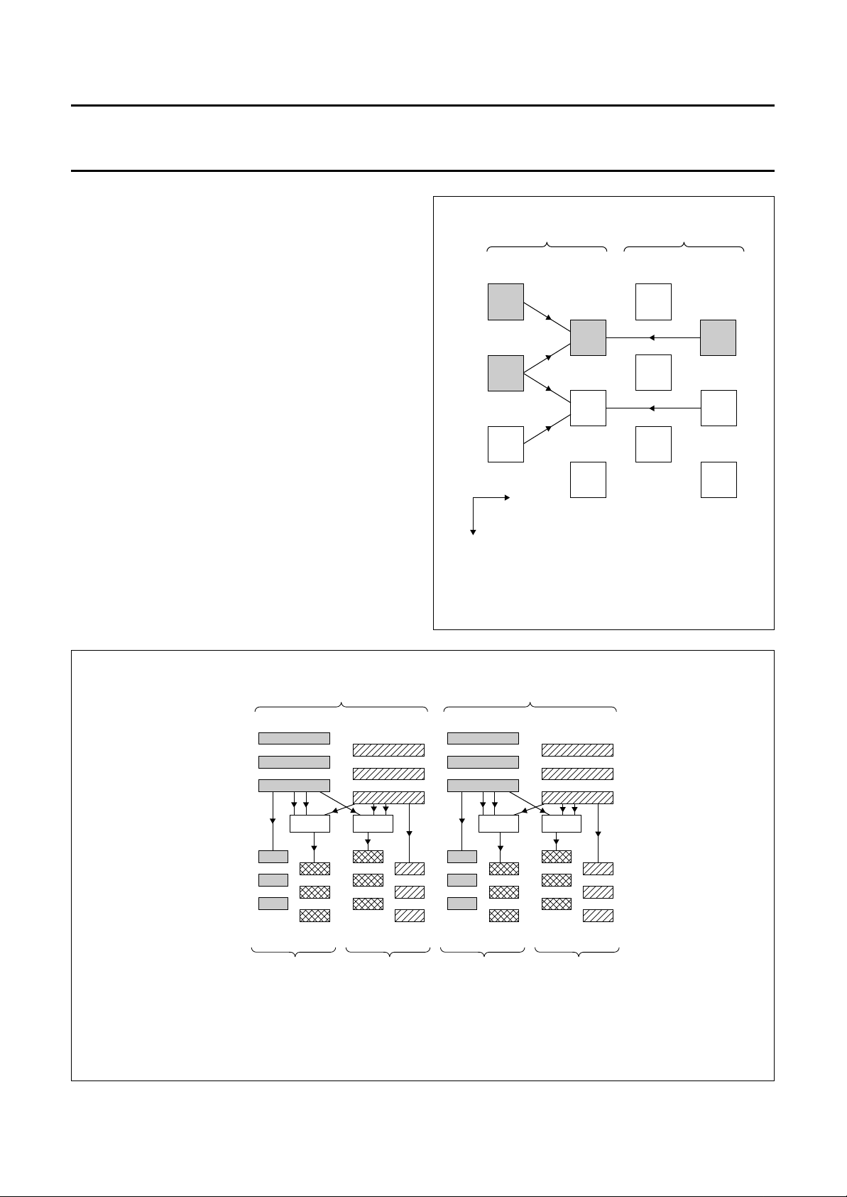
D
EFINITIONS
Framel: l is the number of an input/output frame
temporarily combinating an A and B field.
x
: x is the field raster where A means an odd field and
Field
n
B means an even field.
Frame
combinating an origin/interpolated A and B field;
k indicates the origin input field with
k = 1: odd input field and raster A
k = 2: even input field and raster B within framel.
Field
2 lines of field
(see Fig.3); x is the field raster where A means an odd field
and B means an even field.
: l is the number of an output frame temporarily
l, k
x
: n, m = lines of field
n, m
and 1 line of fieldm using the median filter
n
are interpolated by
n, m
field
n
frame
A
t
handbook, halfpage
y
Fig.3 Generation of (median filter).field
l, k = 1
field
n,m
SAA4990H
frame
l, k = 2
B
B
n, m
A
field
m,n
B
field
m
MGE026
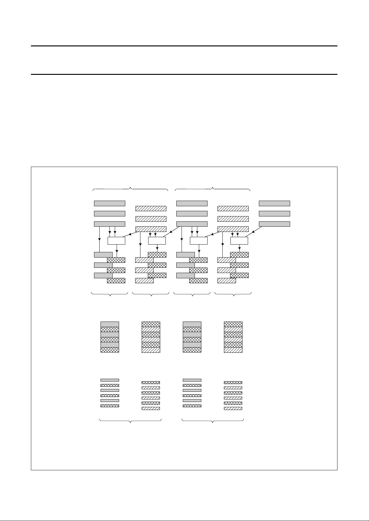
handbook, full pagewidth
input
1fH, 1f
output
2fH, 2f
v
v
field
1
A
frame
field
1
median
field
1, 2
frame
1
A
1, 1
B
field
2, 1
field
2
median
A
frame
B
field
2
1, 2
B
field
3
Fig.4 Scan rate up-conversion.
A
frame
field
3
median
A
B
field
3, 4
2, 1
frame
2
median
A
field
4, 3
frame
field
4
B
field
4
2, 2
MGE027
B
1996 Oct 25 7
Page 8
Philips Semiconductors Preliminary specification
Progressive scan-Zoom and Noise
reduction IC (PROZONIC)
Progressive scan
Progressive scan conversion produces a double number
of lines per field on the output. The field frequency is not
changed, while the line frequency is doubled.
Processing for progressive scan is different for two
successive output fields, e.g. the first output field has a
median operation on the odd lines, while the second has
the median operation on the even lines.
ROGRESSIVE SCAN CONVERSION
P
handbook, full pagewidth
output
1fH, 1f
field
1
v
frame
1
A
field
2
B
SAA4990H
NON-INTERLACE MODE
With non-interlaced progressive scan output, line flicker is
removed because interlace is removed.
I
NTERLACE MODE
With interlaced progressive scan the output line structure
and line flicker is less visible (projection TV).
frame
2
field
3
A
field
4
B
field
5
A
output
2fH, 1f
v
field
1
A
median
frame
B
field
1, 2
1, 1
field
2
B
median
frame
A
field
2,3
1, 2
field
3
A
frame
a. Non-interlaced output; (625/50/1:1) or (525/60/1:1):
frame
1, 1
frame
1, 2
frame
b. Interlaced output; (1250/50/2:1) or (1050/60/2:1):
1
B
field
1,2
field
2,1
A
field
1,1
frame
median
field
3, 4
2, 1
2, 1
A
B
frame
field
4
2
B
frame
frame
field
2,2
median
field
4,5
2, 2
2, 2
B
A
MGE028
Fig.5 Progressive scan conversion.
1996 Oct 25 8
Page 9
Philips Semiconductors Preliminary specification
Progressive scan-Zoom and Noise
reduction IC (PROZONIC)
Noise and cross-colour reduction
The noise reduction is field recursive with an average ratio
between fresh and over previous fields averaged
luminance and chrominance.
Two operating modes can be used in principal: the fixed
and the adaptive mode (see Table 6).
In the fixed mode, the averaging produces a constant
linear combination of the inputs. Except for k = 1, the fixed
mode should not be used for normal operation, because of
its smearing effects.
In the adaptive mode, the averaging ratio switches softly
on the basis of absolute differences in luminance among
the inputs. When the absolute difference is low, only a
small part of the fresh data will be added. When the
difference is high, much of the fresh data will be taken.
This occurs in either the situation of movement or where a
significant vertical contrast is seen.
SAA4990H
To latter remark, note that recursion is done over a field,
and the pixel positions one field apart always have a
vertical offset of one frame line. So averaging is not only
done in the dimension of time but also in the vertical
direction. Therefore averaging vertically on e.g. a vertical
black to white edge would provide a grey result if this was
not adapted for.
The averaging in chrominance is slaved to the luminance
averaging. This implies that differences in the
chrominance are not taken into account for the k-factor
setting.
The noise reduction scheme effectively decreases both
noise and cross-colour patterns.
The cross-colour pattern does not produce an increase of
the measured luminance difference, therefore this pattern
will be averaged over many fields.
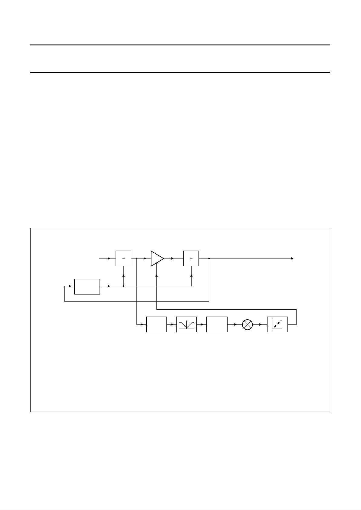
handbook, full pagewidth
(1) Y
(2) see Table 9.
(3) see Fig.11.
out=YA
×k+YB×(1 −k).
FIELD
MEMORY
Y
A
Y
B
k
TF2TF1
FILTER LIMITER FILTER MULTIPLIER
(2)
Y
k-CURVE
(3)
out
(1)
MGE029
Fig.6 Noise reduction scheme.
1996 Oct 25 9
Page 10

Philips Semiconductors Preliminary specification
Progressive scan-Zoom and Noise
reduction IC (PROZONIC)
Vertical sample rate conversion
The variable vertical sample rate conversion is performed
on top of the noise reduced and progressively scanned
data.
The vertical sample rate conversion is intended to cope
with the various letter box formats, to be displayed on
displays with e.g. 16:9 aspect ratio. For this sample rate
conversion, which usually has both a vertical and a
horizontal component, the vertical sample rate conversion
is taken care of in the PROZONIC, while the horizontal
compression can be done in e.g. TDA8753A or
SAA4995WP.
The vertical sample rate conversion can also be used to
convert from an NTSC 525 lines source to a 625 line
display, by setting a vertical sample rate conversion factor
6
⁄5 and necessarily some line-time reduction.
of
Conversion from 625 to 525 lines is possible with
progressive scan output, by setting a vertical sample rate
conversion of5⁄6.
The principle of vertical sample rate conversion is based
on linear interpolation from two successive lines of video in
a frame to produce an output line in either a field or a
frame.
The vertical sample rate conversion factor can be switched
to the following settings for increasing the number of
output lines w.r.t. the number of input lines; see Table 1.
Table 1 Vertical sample rate conversion factor
INPUT LINES OUTPUT LINES FACTOR
2 2 1.00
14 16 1.14
12 14 1.16
10 12 1.20
8 10 1.25
6 8 1.33
10 14 1.40
4 6 1.50
10 16 1.60
6 10 1.67
8 14 1.75
2 4 2.00
SAA4990H
Movie phase detection
While processing video, that was originally film
(25 movement phases per second in the case of 50 Hz
field rates), median filtering is not needed when fields are
combined that have the same movement phase. As this
phase is not generally known, the PROZONIC has a
detection circuit to help determine it. The detection is
based on measurement of absolute luminance differences
between successive input fields, pixel by pixel. These
differences are summed over all active video and give a
number every field. In case of video from film with sufficient
movement, the measured number will alternately be HIGH
and LOW. With the controlling microcontroller, this data
can be filtered appropriately to switch to movie processing
in the correct phase.
The PROZONIC has a provision to generate a rectangular
box, which is position and size programmable. This box
can be used to enable the measurement in the movie
phase detection circuit, only within this rectangle.
Otherwise, the active video part in a field is marked with a
derivative of the RE pulse.
Box generation
A rectangular box is defined by the coordinates of the
left-upper edge (hor_start_box, vert_start_box) and the
right-lower edge (hor_stop_box, vert_stop_box). The
reference for the coordinates are the HD positive edge
(with some processing delay) for the horizontal direction
and the VD positive edge for the vertical.
The box can serve the following purposes:
• Switch between adaptive and fixed k in noise reduction.
If k-fixed is set to 0, then the box switches between
adaptive noise reduced and fully still picture areas. This
provides an option for producing multi picture (still)
images. If no noise reduction is desired in the area
where NR is adaptive, the adaptive setting can be
programmed with k steps to all zeros.
• Switch the movie phase detect measurement to a
defined area of the video.
Decreasing the number of lines on the display w.r.t. the
number of input lines is only possible with progressive
scan output.
1996 Oct 25 10
Page 11

Philips Semiconductors Preliminary specification
Progressive scan-Zoom and Noise
reduction IC (PROZONIC)
handbook, halfpage
vert_start_box
vert_stop_box
hor_start_box
Fig.7 Box dimensions and position.
Control and microcontroller (SNERT-) interface
hor_stop_box
MGE033
SAA4990H
RE2
Read enable for FM2, processed from RE by PROZONIC.
WE2
Write enable for FM2, processed from RE by PROZONIC.
H
O
Holds the writing of the LC display when active.
AUX
Spare output from line-sequencer.
VD
Field frequent reset signal, used in PROZONIC to reset
line counting for boxing. The rising edge of VD is taken as
reference. This may be the display related vertical pulse.
SNRST
C
ONTROL SIGNALS
CK
Line-locked clock of nominal 27 or 32 MHz. This is the
system clock, nominally 864 or 1024 × fh, where fh is the
line frequency. Within the PROZONIC, CK is distributed to
different blocks.
HD
Horizontal reference signal. This signal defines with its
rising edge the start phase of the UV 4 :1:1 format. If the
HD signal has a period equal to 4 clock periods, the UV
data will remain in phase without disruptions, once it has
become in phase. For any mismatch between the applied
HD to the UV data phase, an appropriate HD delay can be
set in the PROZONIC. HD is also used to count lines for
boxing.
RE
Master read enable from memory controller or
ECOBENDIC. This signal controls the memory read
enable if only one field memory is present. To control two
field memories, the PROZONIC generates RE1, RE2 and
WE2 from RE. The vertical sample rate conversion
function has a major influence on these signals.
Field frequent asynchronous reset signal, used in
PROZONIC to reset the communication with
microcontroller. After the rising edge of SNRST,
communication is in its defined state. SNRST is also used
to define the initial phase of the line-sequencer.
SNCL
microcontroller interface clock signal. This signal is
transferred asynchronous to CK by a microcontroller
(UART of 8051 family, mode 0) as communication clock
signal at a frequency of 1 MHz.
SNDA
microcontroller interface data signal. This signal is
transferred or received (asynchronous to CK) by a
microcontroller (UART of 8051 family, mode 0) as
communication data signal at 1 MBaud, related to SNCL.
XTERNAL CONTROL
E
The PROZONIC is controlled via the microcontroller
(SNERT) interface, by sending an address byte and a data
byte to it, with the controllable items as in the register
descriptions in Tables 2 and 3.
RE1
Read enable for FM1, processed from RE by PROZONIC.
1996 Oct 25 11
Page 12

Philips Semiconductors Preliminary specification
Progressive scan-Zoom and Noise
reduction IC (PROZONIC)
Table 2 Write registers
REGISTER BIT NAME FUNCTION
Register 10H to 13H (Kstep)
1
10H 0 to 3 Kstep0 step in adaptive curve from k =
4 to 7 Kstep1 step in adaptive curve from k =
11H 0 to 3 Kstep2 step in adaptive curve from k =
4 to 7 Kstep3 step in adaptive curve from k =
12H 0 to 3 Kstep4 step in adaptive curve from k =
4 to 7 Kstep5 step in adaptive curve from k =
13H 0 to 3 Kstep6 step in adaptive curve from k =
4 to 7 Kstep7 step in adaptive curve from k =
Register 14H (fixed_k)
14H 0 to 3 fixed_k determines k value in fixed k mode; see Table 8
4 to 5 mult weighting of TF2 output; see Table 9
6 _upbox microcontroller (_upbox = 0) or box controlled (_upbox = 1); see Table 6
7 _adfix adaptive (_adfix = 0) or fixed k (_adfix = 1); see Table 6
⁄16to k =1⁄8; weight of 1
1
⁄8to k =2⁄8; weight of 1
2
⁄8to k =3⁄8; weight of 2
3
⁄8to k =4⁄8; weight of 2
4
⁄8to k =5⁄8; weight of 4
5
⁄8to k =6⁄8; weight of 4
6
⁄8to k =7⁄8; weight of 8
7
⁄8to k =8⁄8; weight of 8
SAA4990H
Register 15H (Tfilter)
15H 0 to 1 Tfilter1_select determines filter1 characteristic; see Table5
2 to 7 Tfilter2_select determines filter2 characteristic; see Table7
Register 16H (hor_start_box)
16H 0 to 7 hor_start_box horizontal start position of box w.r.t. picture
Register 17H (hor_stop_box)
17H 0 to 7 hor_stop_box horizontal stop position of box w.r.t. picture
Register 18H and 19H (vert_start_box)
18H (bit 8 = 0) 0 to 7 vert_start_box vertical start position of box w.r.t. picture; bit 8 (MSB) is encoded in the
19H (bit 8 = 1)
address
Register 1AH and 1BH (vert_stop_box)
1AH (bit 8 = 0) 0to7 vert_stop_box vertical stop position of box w.r.t. picture; bit 8 (MSB) is encoded in the
1BH (bit 8 = 1)
address
Register 1CH (box generation and UV processing)
1CH 0 UV8bit U/V signals are taken from input as 8-bit values instead of 7-bit
1 UVbin U/V signals are taken from input as binary signals instead of
twos complement
2 inv_box inversion of box signal (inv_box = 1)
3 en_box overall enable box signal
4 en_box_mpd enable box signal to define movie phase detection area
5 boxPSC box generation for progressive scan with more than 511 lines
6, 7 reserved
Register 1DH (reserved)
1996 Oct 25 12
Page 13

Philips Semiconductors Preliminary specification
Progressive scan-Zoom and Noise
SAA4990H
reduction IC (PROZONIC)
REGISTER BIT NAME FUNCTION
Register 1EH (horizontal delay)
1EH 0 to 2 in_del programmable horizontal delay (0 to 7 clock periods) of the luminance data
input in comparison to the U/V data input (from FM1)
3, 4 HD_del determines 1 to 4 clock pulse shift for horizontal reference HD
5, 6 WE2_del determines 1to4 clock pulse shift for WE2 output
7 reserved
Register 1FH (sequence data)
1
1FH 0 to 2 mix setting of mixer to 0,
of line sequencer
3 post_zoom setting of multiplexer pre or post LM_zoom to MIX; setting per line in
1 to 16 lines of line sequencer
4 post_lfr setting of multiplexer pre or post LM_lfr to MIX; setting per line in
1 to 16 lines of line sequencer
5 mem_hold setting of field and line memory hold; setting per line in 1 to 16 lines of line
sequencer
6 o_hold setting of output hold, may stop e.g. LC display; setting per line in
1 to 16 lines of line sequencer
7 aux setting of auxiliary sequencer output signal; setting per line in 1 to 16 lines
of line sequencer
⁄4,1⁄4,1⁄2,1⁄2,3⁄4,3⁄4, 1; setting per line in 1 to 16 lines
Register 20H (sequence length)
20H 0 to 3 seq_length setting of sequence length to 1, 2, 3 to 16 lines
4 to 7 reserved
Register 21H (field control 1); note 1
21H 0 FCM4 see Fig.12 and Table 10
1 FCM23
2 FCM1
3, 4 fixselUV defines UV data output; see Fig.12 and Table 11
5, 6 fixselY defines Y data output; see Fig.12 and Table 11
7 RAM1wr selects RAM1 for write operation; note 2; see Fig.13
Register 22H (field control 2); note 1
22H 0 WE2act activates field controlled write enable 2 for FM2
1, 2 RE1del line delay for read enable 1 (FM1) w.r.t. RE input (pin 39)
3, 4 RE2del line delay for read enable 2 (FM2) w.r.t. RE input (pin 39)
5, 6 WE2del line delay for write enable 2 (FM2) w.r.t. RE input (pin 39)
7 UV_av UV averaged while luminance signal is median filtered
Notes
1. Data will be active after next VD pulse (pin 40).
2. In normal conditions control bit should be toggled field by field.
1996 Oct 25 13
Page 14

Philips Semiconductors Preliminary specification
Progressive scan-Zoom and Noise
reduction IC (PROZONIC)
Table 3 Read registers
REGISTER BIT NAME
Register 26H (MPD_LSB)
26H 0 to 7 MPD_LSB
Register 27H (MPD_MSB)
27H 0 to 7 MPD_MSB
Table 4 Output multiplex control
output_mux[2:0] THROUGHPUT
000 video
011 grey
111 sawtooth
Table 5 Filter1 characteristic
Tfilter1_select[1:0] Tfilter1-TRANSFER (z)
00 1
1
01
10
11
⁄2× z+1+1⁄2×z
1
⁄
2
1
⁄2× z+1⁄2+1⁄2×z
−1
−1
SAA4990H
Table 6 Adaptive/fixed_k selection
Dynamic box signal, active in user defined rectangular
part of the picture, enable with en_box, may be inverted
with inv_box.
_upbox _adfix box k
00X
00X
01X
01X
1X
1X
1X
1X
(1)
(1)
(1)
(1)
Note
1. X = don’t care bits.
(1)
(1)
(1)
(1)
adapt
adapt
fixed
fixed
0 fixed
1 adapt
0 fixed
1 adapt
TF1(z) =1⁄2z+a+1⁄2z−1.
(1) a = 1.
(2) a =1⁄2.
15
handbook, halfpage
10
IH_TF1I
5
(dB)
0
−5
−10
−15
−20
−25
MGE035
(1)
(2)
1/4 f
s
Fig.8 Characteristic pre-filter TF1.
1/2 f
s
1996 Oct 25 14
Page 15

Philips Semiconductors Preliminary specification
Progressive scan-Zoom and Noise
reduction IC (PROZONIC)
Table 7 Filter2 characteristic
Tfilter2_select[5:0]
HEX DECIMAL
00 00
01 01 1 × z2+1⁄2× z+1+1⁄2×z−1+1×z
02 02 0 × z2+1⁄2× z+1+1⁄2×z−1+0×z
04 04
05 05 1 × z2+1×z+1+1×z−1+1×z
06 06 0 × z2+1×z+1+1×z−1+0×z
08 08
09 09 1 × z2+0×z+1+0×z−1+1×z
0A 10 0 × z2+0×z+1+0×z−1+0×z
10 16
11 17 1 × z2+1⁄2× z+2+1⁄2×z−1+1×z
12 18 0 × z2+1⁄2× z+2+1⁄2×z−1+0×z
14 20
15 21 1 × z2+1×z+2+1×z−1+1×z
16 22 0 × z2+1×z+2+1×z−1+0×z
18 24
19 25 1 × z2+0×z+2+0×z−1+1×z
1A 26 0 × z2+0×z+2+0×z−1+0×z
20 32
21 33 1 × z2+1⁄2× z+0+1⁄2×z−1+1×z
22 34 0 × z2+1⁄2× z+0+1⁄2×z−1+0×z
24 36
25 37 1 × z2+1×z+0+1×z−1+1×z
26 38 0 × z2+1×z+0+1×z−1+0×z
28 40
29 41 1 × z2+0×z+0+0×z−1+1×z
2A 42 0 × z2+0×z+0+0×z−1+0×z
1
1
1
1
1
1
1
1
1
Tfilter2-TRANSFER (z)
⁄2× z2+1⁄2× z+1+1⁄2×z−1+1⁄2×z
−2
−2
⁄2× z2+1×z+1+1×z−1+1⁄2×z
⁄2× z2+0×z+1+0×z−1+1⁄2×z
−2
−2
−2
−2
−2
−2
⁄2× z2+1⁄2× z+2+1⁄2×z−1+1⁄2×z
−2
−2
⁄2× z2+1×z+2+1×z−1+1⁄2×z
⁄2× z2+0×z+2+0×z−1+1⁄2×z
−2
−2
−2
−2
−2
−2
⁄2× z2+1⁄2× z+0+1⁄2×z−1+1⁄2×z
−2
−2
⁄2× z2+1×z+0+1×z−1+1⁄2×z
⁄2× z2+0×z+0+0×z−1+1⁄2×z
−2
−2
−2
−2
−2
−2
SAA4990H
−2
−2
−2
1996 Oct 25 15
Page 16

Philips Semiconductors Preliminary specification
Progressive scan-Zoom and Noise
reduction IC (PROZONIC)
15
handbook, halfpage
10
IH_TF2I
5
(dB)
0
−5
−10
−15
−20
−25
(1)
(2)
1/4 f
s
MGE036
1/2 f
s
15
handbook, halfpage
10
IH_TF2I
5
(dB)
0
−5
−10
−15
−20
−25
(2)
(1)
1/4 f
SAA4990H
s
MGE037
1/2 f
s
TF2(z) = a z2+bz+2c+bz−1+az−2.
(1) c = 0.
(2) c = 1.
Fig.9 Characteristic pre-filter TF2 (a = 0; b = 1).
Table 8 Fixed_k setting
Fixed_k SETTING [3:0]
HEX DECIMAL
00 00 0
01 01
02 02
03 03
04 04
05 05
06 06
07 07
08 08
09 09
0A 10
0B 11
0C 12
0D 13
0E 14
0F 15
TF2(z) = a z2+bz+2c+bz−1+az−2.
(1) b = 1.
(2) b = 0.
Fig.10 Characteristic pre-filter TF2 (a = 1; c = 1).
Table 9 Mult setting
MULT SETTING [1:0]
k
FACTOR
HEX DECIMAL
00 00 1
1
⁄
16
2
⁄
16
3
⁄
16
4
⁄
16
5
⁄
16
6
⁄
16
7
⁄
16
8
⁄
16
9
⁄
16
10
⁄
16
11
⁄
16
12
⁄
16
13
⁄
16
14
⁄
16
16
⁄
16
01 01 2
02 02 4
03 03 8
1996 Oct 25 16
Page 17

Philips Semiconductors Preliminary specification
Progressive scan-Zoom and Noise
reduction IC (PROZONIC)
handbook, full pagewidth
1
14/16
k
12/16
10/16
8/16
6/16
4/16
2/16
0
SAA4990H
MGE034
9080706050403020101
input amplitude
128120110100
Fig.11 k factor curve (example) from filter TF2 and multiplier (see Fig.6).
handbook, full pagewidth
FM1
a
MUX1 LM1
b
FM2
FCM1
FM1 and FM2: field memories (external).
LM1 and LM2: line memories.
a
MUX2
b
a
MUX3
b
CONTROL LOGIC
FCM23
a
MUX4
b
FCM4
LM2
MEDIAN (Y)
or
MULTIPLEXER (UV)
fixselY
fixselUV
data
output
MGE030
Fig.12 Extract of the Progressive scan-Zoom and Noise reduction IC (PROZONIC) data path.
1996 Oct 25 17
Page 18

Philips Semiconductors Preliminary specification
Progressive scan-Zoom and Noise
SAA4990H
reduction IC (PROZONIC)
Table 10 Field controlled output
FCM23
(1)
FCM1
(2)
FCM4
0 X 0 X FM1 FM2 FM1
0 X 1 X FM1 FM2 FM2
1 0 0 FM2 FM1 FM2/1H delay FM1
1 0 1 FM2 FM1 FM2/1H delay FM2/1H delay
1 1 0 FM1 FM1/1H delay FM2 FM1/1H delay
1 1 1 FM1 FM1/1H delay FM2 FM2
Notes
1. FCM23 is the field controlled MUX2, MUX3.
2. FCM1 is the field controlled MUX1.
3. FCM4 is the field controlled MUX4.
Table 11 Data output
fixselY/fixselUV
HEX DECIMAL
00 00 MUX2
01 01 MUX4/1H delay
02 02 MUX3
03 03 MEDIAN (Y)/median controlled MULTIPLEXER (UV)
FIELD CONTROLLED OUTPUT TO MEDIAN (Y) OR MUL TIPLEXER (UV)
(3)
MUX1 MUX2 MUX3 MUX4
DATA OUTPUT FROM
handbook, full pagewidth
from SNERT
register
R/W control
(RAM1wr)
(1) n = sequence length + 1
RAM1
sequence data 1
sequence data 2
sequence data n
RAM2
sequence data 1
sequence data 2
sequence data n
Fig.13 Internal RAM control.
1996 Oct 25 18
to
to
(1)
to internal
processing
(1)
MGE031
Page 19

Philips Semiconductors Preliminary specification
Progressive scan-Zoom and Noise
reduction IC (PROZONIC)
Microcontroller interface (SNERT)
In the microcontroller interface the external signals SNDA
and SNCL are processed to address and data. Data
enable pulses are derived from the received addresses.
The data enable pulses are used elsewhere for input
enabling the delivered data into various control registers.
The microcontroller interface operates in a few stages:
1. SNCL positive and negative edges are sampled
2. on each negative edge of SNCL and SNDA data is
shifted in a shift register
3. starting from phase 0, a counter counts positive edges
of SNCL
4. during phase 7, but waited for a negative edge of
SNCL, so after the 8th negative edge of SNCL, an
address latch enable pulse is made, whereby the shift
register contents are taken over in the address register
5. in the address range 10H to 27H, the addresses are
decoded in two steps
6. during phase 15, but waited for a negative edge of
SNCL, so after the 16th negative edge of SNCL, the
address has been decoded and will be passed to any
of the data enable pulses.
SAA4990H
For each of the functions vert_start_box and
vert_stop_box, two addresses are used, in which the LSB
from the address is taken as an extra MSB for the data.
This is done because vert_start_box and vert_stop_box
must be supplied with 9-bit data. All other data from the
SNERT-bus has only relevance in the 7:0 range.
During the data phases (phase 8 to 15), each negative
edge produces a shift pulse for the movie phase detect
circuit that produces output data on the SNDA signal. The
data enables for the movie phase detect circuit are active
in all of the data phases, when an address 26 or 27 has
been decoded.
After an MPD read transmission it is necessary to send a
second (dummy) transmission to the PROZONIC.
LIMITING VALUES
In accordance with the Absolute Maximum Rating System (IEC 134).
SYMBOL PARAMETER MIN. MAX. UNIT
V
V
V
T
T
I
DDD
DDA
stg
amb
input voltage −0.5 +7 V
digital supply voltage −0.5 +7 V
analog supply voltage −0.5 +7 V
storage temperature −65 +150 °C
operating ambient temperature 0 70 °C
1996 Oct 25 19
Page 20

Philips Semiconductors Preliminary specification
Progressive scan-Zoom and Noise
SAA4990H
reduction IC (PROZONIC)
CHARACTERISTICS
V
= 4.5 to 5.5 V; T
DDD
SYMBOL PARAMETER CONDITIONS MIN. MAX. UNIT
Supply
V
I
DDD
DDD
supply voltage 4.5 5.5 V
supply current − 180 mA
Digital inputs
V
IL
LOW level input voltage except CK −0.5 +0.8 V
LOW level input voltage for CK −0.5 +0.6 V
V
IH
HIGH level input voltage except CK 2.0 V
HIGH level input voltage for CK 2.4 V
I
LI
C
I
input leakage current − 10 µA
input capacitance − 10 pF
Digital outputs
V
OH
V
OL
HIGH level output voltage note 1 2.4 V
LOW level output voltage note 1 0 0.6 V
Timing
T
cyCK
δ
CK
t
r
t
f
t
SU
t
HD
t
OH
t
OD
CK cycle time 27 − ns
CK duty factor t
CK rise time − 5ns
CK fall time − 6ns
input data set-up time − 3ns
input data hold time − 3ns
output data hold time note 1 3 − ns
output data delay time note 1 − 23 ns
Data output loads (3-state outputs)
C
L
output load capacitance 10 20 pF
output load capacitance for RE1, RE2, WE2
and SNDA
= 0 to 70 °C; unless otherwise specified.
amb
CKH/tCKL
+ 0.5 V
DDD
+ 0.5 V
DDD
DDD
V
40 60 %
10 35 pF
Note
1. Timings and levels have to be measured with load circuits 1.2 kΩ connected to 3.0 V (TTL load) and C
1996 Oct 25 20
=20pF.
L
Page 21

Philips Semiconductors Preliminary specification
Progressive scan-Zoom and Noise
reduction IC (PROZONIC)
Input/output timing
handbook, full pagewidth
CLOCK
CK1, CK2
INPUT
DATA
t
r
t
HD
t
SU
T
cyCKH
T
cyCK
SAA4990H
t
f
2.4 V
1.5 V
0.6 V
2.0 V
0.8 V
OUTPUT
DATA
t
OD
t
OH
Fig.14 Timing diagram.
2.4 V
0.6 V
MGE032
1996 Oct 25 21
Page 22

Philips Semiconductors Preliminary specification
Progressive scan-Zoom and Noise
reduction IC (PROZONIC)
APPLICATION INFORMATION
The basic application of PROZONIC in a feature box is
shown in Fig.15. Here, apart from the data streams, the
‘timed control data’ streams indicate that some memory
control signals have to be processed by the PROZONIC,
in order to let the vertical sample rate conversion function
correctly.
Horizontal scaling factors are performed by the memory
controller SAA4951WP/SAA4952H.
All basic clock signals in the feature box are provided by
the memory controller, nominal frequencies on the double
scan parts of the system are 27, 32 or 36 MHz. In any case
the display frequency is decoupled from the acquisition
clock.
The memory controller supplies the deflection processor
with clock, horizontal and vertical pulses.
The SNERT-bus is used to control the PROZONIC at a
data rate of typically 1 Mbits/s.
SAA4990H
Table 12 Abbreviations used in Fig.15
BLND horizontal blanking signal, display related
HDFL horizontal synchronization signal, deflection
related
HA horizontal synchronization signal, acquisition
related
HRA horizontal reference signal, acquisition related
HRD horizontal reference signal, display related
HRDFL horizontal reference signal, deflection related
IE input enable signal
LLA line locked clock signal, acquisition related
LLD line locked clock signal, display related
LLDFL line locked clock signal, deflection related
RE read enable signal
RSTR reset read signal
RSTW reset write signal
2
SCL serial clock signal (I
SDA serial data signal (I
SNERT synchronous no parity eight bit reception and
transmission (serial control bus)
SRC serial read clock signal
SWC serial write clock signal
VA vertical synchronization signal,
acquisition related
VDFL vertical synchronization signal,
deflection related
C-bus)
2
C-bus)
1996 Oct 25 22
Page 23

Philips Semiconductors Preliminary specification
Progressive scan-Zoom and Noise
reduction IC (PROZONIC)
handbook, full pagewidth
10nF220
Y
in
3
−(R−Y)
in
9
−(B−Y)
in
7
18 nF
5
33 nF
11
33 nF
6,23,
12
32
+5 V
1.5
220
µF
nF
nF
41328
ADC
TDA8755
10,
18
1615 17
24
25
26
27
28
29
30
31
19
20
21
22
C0
6
C1
7
C2
8
C3
9
C4
10
C5
11
C6
12
C7
13
C8
2
C9
3
C10
4
C11
5
0
9
1
8
2
7
3
6
4
5
5
4
6
3
7
2
8
13
9
12
10
11
11
10
+5 V
18,19,201,36 16,17
FM 2
TMS4C2970
15,22 14,23
+5 V
18,19,201,36 22 23 21
FM 1
TMS4C2970
14
15 17 16
SWC RSTW WE IE
SAA4990H
WE2
RE2
B0
B10
B11
SRC
RE1
A10
A11
24
29
B1
30
B2
31
B3
32
B4
35
B5
36
B6
37
B7
38
B8
25
B9
26
27
28
40,60
20
3
A0
76
A1
75
A2
72
A3
71
A4
70
A5
69
A6
68
A7
67
A8
80
A9
79
78
77
39
RE
21
31
30
29
28
27
26
25
24
35
34
33
32
RSTR
28
29
30
31
32
33
34
35
24
25
26
27
n.c.
63,64,
23
65,66
PROZONIC
SAA4990H
5,12,22,33,45
1,2,4,11,21,34
46,52,59,73
41 62 61
12 12
51,58,74
C0
15
C1
14
C2
13
C3
10
C4
9
C5
8
C6
7
C7
6
C8
19
C9
18
C10
17
C11
16
+5 V
D0
D1
D2
D3
D4
D5
D6
D7
D8
D9
D10
D11
9,25,
45
40,62,
65,66
46
47
48
49
50
51
52
41
42
43
44
26 19 23 24
48
49
50
53
54
55
56
57
42
43
44
47
SNERT
+5 V
60,63,
68
BENDIC
SAA7158
0
10 kΩ
598,27,
Y
out
61
−(R−Y)
out
67
−(B−Y)
out
64
100 nF
54
100 nF
57
20,21,
22
BLND
2
10
6
18
3428 7 4
12,24,34,44
2,10,23,36
+5 V
VA
HA
39
137 11 35 33 13 43 38
HDFL HRD HRA HRDFL LLDFL LLA LLD
ECO 3
SAA4951
DEFLECTION PLL
ACQUISITION PLL
DISPLAY PLL
20
0
25
1
26
2
27
3
28
4
29
5
30
6
31
7
32
8
21
9
22
21311
43
42
41
40
39
38
37
36
33
18,19
µC
S87C654
15 14 20 21
22 pF 22 pF
35,44
22
10
8
9
12 MHz
MGE025
+5 V
2.2 µF
SCL
SDA
VDFL
LLDFL
HDFL
Fig.15 Application circuit.
1996 Oct 25 23
Page 24

Philips Semiconductors Preliminary specification
Progressive scan-Zoom and Noise
reduction IC (PROZONIC)
PACKAGE OUTLINE
QFP80: plastic quad flat package; 80 leads (lead length 1.95 mm); body 14 x 20 x 2.8 mm
c
y
X
64 41
65
40
A
Z
E
SAA4990H
SOT318-2
pin 1 index
80
1
w M
b
0.25
p
D
H
D
cE
0.25
0.14
D
20.1
19.9
p
0.45
0.30
0 5 10 mm
(1)
(1) (1)(1)
14.1
13.9
e
DIMENSIONS (mm are the original dimensions)
mm
A
max.
3.2
0.25
0.05
2.90
2.65
UNIT A1A2A3b
Note
1. Plastic or metal protrusions of 0.25 mm maximum per side are not included.
24
Z
D
scale
eH
H
24.2
0.8 1.95
23.6
25
D
e
H
E
E
w M
b
p
v M
A
B
v M
B
LLpQZywv θ
E
18.2
17.6
1.0
0.6
1.4
1.2
A
2
A
A
1
detail X
0.20.2 0.1
Q
(A )
3
θ
L
p
L
Z
E
D
1.2
0.8
o
7
o
0
1.0
0.6
OUTLINE
VERSION
SOT318-2
IEC JEDEC EIAJ
REFERENCES
1996 Oct 25 24
EUROPEAN
PROJECTION
ISSUE DATE
92-12-15
95-02-04
Page 25

Philips Semiconductors Preliminary specification
Progressive scan-Zoom and Noise
reduction IC (PROZONIC)
SOLDERING
Introduction
There is no soldering method that is ideal for all IC
packages. Wave soldering is often preferred when
through-hole and surface mounted components are mixed
on one printed-circuit board. However, wave soldering is
not always suitable for surface mounted ICs, or for
printed-circuits with high population densities. In these
situations reflow soldering is often used.
This text gives a very brief insight to a complex technology.
A more in-depth account of soldering ICs can be found in
our
“IC Package Databook”
Reflow soldering
Reflow soldering techniques are suitable for all QFP
packages.
The choice of heating method may be influenced by larger
plastic QFP packages (44 leads, or more). If infrared or
vapour phase heating is used and the large packages are
not absolutely dry (less than 0.1% moisture content by
weight), vaporization of the small amount of moisture in
them can cause cracking of the plastic body. For more
information, refer to the Drypack chapter in our
Reference Handbook”
Reflow soldering requires solder paste (a suspension of
fine solder particles, flux and binding agent) to be applied
to the printed-circuit board by screen printing, stencilling or
pressure-syringe dispensing before package placement.
Several techniques exist for reflowing; for example,
thermal conduction by heated belt. Dwell times vary
between 50 and 300 seconds depending on heating
method. Typical reflow temperatures range from
215 to 250 °C.
(order code 9398 652 90011).
“Quality
(order code 9397 750 00192).
SAA4990H
If wave soldering cannot be avoided, the following
conditions must be observed:
• A double-wave (a turbulent wave with high upward
pressure followed by a smooth laminar wave)
soldering technique should be used.
• The footprint must be at an angle of 45° to the board
direction and must incorporate solder thieves
downstream and at the side corners.
Even with these conditions, do not consider wave
soldering the following packages: QFP52 (SOT379-1),
QFP100 (SOT317-1), QFP100 (SOT317-2),
QFP100 (SOT382-1) or QFP160 (SOT322-1).
During placement and before soldering, the package must
be fixed with a droplet of adhesive. The adhesive can be
applied by screen printing, pin transfer or syringe
dispensing. The package can be soldered after the
adhesive is cured.
Maximum permissible solder temperature is 260 °C, and
maximum duration of package immersion in solder is
10 seconds, if cooled to less than 150 °C within
6 seconds. Typical dwell time is 4 seconds at 250 °C.
A mildly-activated flux will eliminate the need for removal
of corrosive residues in most applications.
Repairing soldered joints
Fix the component by first soldering two diagonallyopposite end leads. Use only a low voltage soldering iron
(less than 24 V) applied to the flat part of the lead. Contact
time must be limited to 10 seconds at up to 300 °C. When
using a dedicated tool, all other leads can be soldered in
one operation within 2 to 5 seconds between
270 and 320 °C.
Preheating is necessary to dry the paste and evaporate
the binding agent. Preheating duration: 45 minutes at
45 °C.
Wave soldering
Wave soldering is not recommended for QFP packages.
This is because of the likelihood of solder bridging due to
closely-spaced leads and the possibility of incomplete
solder penetration in multi-lead devices.
1996 Oct 25 25
Page 26

Philips Semiconductors Preliminary specification
Progressive scan-Zoom and Noise
SAA4990H
reduction IC (PROZONIC)
DEFINITIONS
Data sheet status
Objective specification This data sheet contains target or goal specifications for product development.
Preliminary specification This data sheet contains preliminary data; supplementary data may be published later.
Product specification This data sheet contains final product specifications.
Limiting values
Limiting values given are in accordance with the Absolute Maximum Rating System (IEC 134). Stress above one or
more of the limiting values may cause permanent damage to the device. These are stress ratings only and operation
of the device at these or at any other conditions above those given in the Characteristics sections of the specification
is not implied. Exposure to limiting values for extended periods may affect device reliability.
Application information
Where application information is given, it is advisory and does not form part of the specification.
LIFE SUPPORT APPLICATIONS
These products are not designed for use in life support appliances, devices, or systems where malfunction of these
products can reasonably be expected to result in personal injury. Philips customers using or selling these products for
use in such applications do so at their own risk and agree to fully indemnify Philips for any damages resulting from such
improper use or sale.
1996 Oct 25 26
Page 27

Philips Semiconductors Preliminary specification
Progressive scan-Zoom and Noise
reduction IC (PROZONIC)
SAA4990H
NOTES
1996 Oct 25 27
Page 28

Philips Semiconductors – a worldwide company
Argentina: see South America
Australia: 34 Waterloo Road, NORTH RYDE, NSW 2113,
Tel. +61 2 9805 4455, Fax. +61 2 9805 4466
Austria: Computerstr. 6, A-1101 WIEN, P.O. Box 213,
Tel. +43 1 60 101, Fax. +43 1 60 101 1210
Belarus: Hotel Minsk Business Center, Bld. 3, r. 1211, Volodarski Str. 6,
220050 MINSK, Tel. +375 172 200 733, Fax. +375 172 200 773
Belgium: see The Netherlands
Brazil: see South America
Bulgaria: Philips Bulgaria Ltd., Energoproject, 15th floor,
51 James Bourchier Blvd., 1407 SOFIA,
Tel. +359 2 689 211, Fax. +359 2 689 102
Canada: PHILIPS SEMICONDUCTORS/COMPONENTS,
Tel. +1 800 234 7381
China/Hong Kong: 501 Hong Kong Industrial Technology Centre,
72 Tat Chee Avenue, Kowloon Tong, HONG KONG,
Tel. +852 2319 7888, Fax. +852 2319 7700
Colombia: see South America
Czech Republic: see Austria
Denmark: Prags Boulevard 80, PB 1919, DK-2300 COPENHAGEN S,
Tel. +45 32 88 2636, Fax. +45 31 57 1949
Finland: Sinikalliontie 3, FIN-02630 ESPOO,
Tel. +358 9 615800, Fax. +358 9 61580/xxx
France: 4 Rue du Port-aux-Vins, BP317, 92156 SURESNES Cedex,
Tel. +33 1 40 99 6161, Fax. +33 1 40 99 6427
Germany: Hammerbrookstraße 69, D-20097 HAMBURG,
Tel. +49 40 23 53 60, Fax. +49 40 23 536 300
Greece: No. 15, 25th March Street, GR 17778 TAVROS/ATHENS,
Tel. +30 1 4894 339/239, Fax. +30 1 4814 240
Hungary: see Austria
India: Philips INDIA Ltd, Shivsagar Estate, A Block, Dr. Annie Besant Rd.
Worli, MUMBAI 400 018, Tel. +91 22 4938 541, Fax. +91 22 4938 722
Indonesia: see Singapore
Ireland: Newstead, Clonskeagh, DUBLIN 14,
Tel. +353 1 7640 000, Fax. +353 1 7640 200
Israel: RAPAC Electronics, 7 Kehilat Saloniki St, TEL AVIV 61180,
Tel. +972 3 645 0444, Fax. +972 3 649 1007
Italy: PHILIPS SEMICONDUCTORS, Piazza IV Novembre 3,
20124 MILANO, Tel. +39 2 6752 2531, Fax. +39 2 6752 2557
Japan: Philips Bldg 13-37, Kohnan 2-chome, Minato-ku, TOKYO 108,
Tel. +81 3 3740 5130, Fax. +81 3 3740 5077
Korea: Philips House, 260-199 Itaewon-dong, Yongsan-ku, SEOUL,
Tel. +82 2 709 1412, Fax. +82 2 709 1415
Malaysia: No. 76 Jalan Universiti, 46200 PETALING JAYA, SELANGOR,
Tel. +60 3 750 5214, Fax. +60 3 757 4880
Mexico: 5900 Gateway East, Suite 200, EL PASO, TEXAS 79905,
Tel. +9-5 800 234 7381
Middle East: see Italy
Netherlands: Postbus 90050, 5600 PB EINDHOVEN, Bldg. VB,
Tel. +31 40 27 82785, Fax. +31 40 27 88399
New Zealand: 2 Wagener Place, C.P.O. Box 1041, AUCKLAND,
Tel. +64 9 849 4160, Fax. +64 9 849 7811
Norway: Box 1, Manglerud 0612, OSLO,
Tel. +47 22 74 8000, Fax. +47 22 74 8341
Philippines: Philips Semiconductors Philippines Inc.,
106 Valero St. Salcedo Village, P.O. Box 2108 MCC, MAKATI,
Metro MANILA, Tel. +63 2 816 6380, Fax. +63 2 817 3474
Poland: Ul. Lukiska 10, PL 04-123 WARSZAWA,
Tel. +48 22 612 2831, Fax. +48 22 612 2327
Portugal: see Spain
Romania: see Italy
Russia: Philips Russia, Ul. Usatcheva 35A, 119048 MOSCOW,
Tel. +7 095 247 9145, Fax. +7 095 247 9144
Singapore: Lorong 1, Toa Payoh, SINGAPORE 1231,
Tel. +65 350 2538, Fax. +65 251 6500
Slovakia: see Austria
Slovenia: see Italy
South Africa: S.A. PHILIPS Pty Ltd., 195-215 Main Road Martindale,
2092 JOHANNESBURG, P.O. Box 7430 Johannesburg 2000,
Tel. +27 11 470 5911, Fax. +27 11 470 5494
South America: Rua do Rocio 220, 5th floor, Suite 51,
04552-903 São Paulo, SÃO PAULO - SP, Brazil,
Tel. +55 11 821 2333, Fax. +55 11 829 1849
Spain: Balmes 22, 08007 BARCELONA,
Tel. +34 3 301 6312, Fax. +34 3 301 4107
Sweden: Kottbygatan 7, Akalla, S-16485 STOCKHOLM,
Tel. +46 8 632 2000, Fax. +46 8 632 2745
Switzerland: Allmendstrasse 140, CH-8027 ZÜRICH,
Tel. +41 1 488 2686, Fax. +41 1 481 7730
Taiwan: PHILIPS TAIWAN Ltd., 23-30F, 66,
Chung Hsiao West Road, Sec. 1, P.O. Box 22978,
TAIPEI 100, Tel. +886 2 382 4443, Fax. +886 2 382 4444
Thailand: PHILIPS ELECTRONICS (THAILAND) Ltd.,
209/2 Sanpavuth-Bangna Road Prakanong, BANGKOK 10260,
Tel. +66 2 745 4090, Fax. +66 2 398 0793
Turkey: Talatpasa Cad. No. 5, 80640 GÜLTEPE/ISTANBUL,
Tel. +90 212 279 2770, Fax. +90 212 282 6707
Ukraine: PHILIPS UKRAINE, 4 Patrice Lumumba str., Building B, Floor 7,
252042 KIEV, Tel. +380 44 264 2776, Fax. +380 44 268 0461
United Kingdom: Philips Semiconductors Ltd., 276 Bath Road, Hayes,
MIDDLESEX UB3 5BX, Tel. +44 181 730 5000, Fax. +44 181 754 8421
United States: 811 East Arques Avenue, SUNNYVALE, CA 94088-3409,
Tel. +1 800 234 7381
Uruguay: see South America
Vietnam: see Singapore
Yugoslavia: PHILIPS, Trg N. Pasica 5/v, 11000 BEOGRAD,
Tel. +381 11 625 344, Fax.+381 11 635 777
For all other countries apply to: Philips Semiconductors, Marketing & Sales Communications,
Building BE-p, P.O. Box 218, 5600 MD EINDHOVEN, The Netherlands, Fax. +31 40 27 24825
© Philips Electronics N.V. 1996 SCA52
All rights are reserved. Reproduction in whole or in part is prohibited without the prior written consent of the copyright owner.
The information presented in this document does not form part of any quotation or contract, is believed to be accurate and reliable and may be changed
without notice. No liability will be accepted by the publisher for any consequence of its use. Publication thereof does not convey nor imply any license
under patent- or other industrial or intellectual property rights.
Internet: http://www.semiconductors.philips.com
Printed in The Netherlands 537021/1200/01/pp28 Date of release: 1996 Oct 25 Document order number: 9397 750 01435
 Loading...