

Page 1

INTEGRATED CIRCUITS
DATA SH EET
SAA4981
Monolithic integrated 16 : 9
compressor
Preliminary specification
Supersedes data of May 1994
File under Integrated Circuits, IC02
1995 Oct 05
Page 2
Philips Semiconductors Preliminary specification
Monolithic integrated 16 : 9 compressor SAA4981
FEATURES
• Fixed horizontal compression by a factor of4⁄3 for most
video standards
• Three fixed screen positions (left, centre and right)
• 5 MHz bandwidth
• Bypass function
• Inputs for luminance and chrominance of side panels
• Standard video inputs and outputs (Y, (B−Y) and (R−Y))
• Horizontal and vertical sync signals are not processed
• Pre filters and post filters on chip.
The synchronisation input HREF is a line frequency
reference signal. The bandwidth of the IC is up to 5 MHz
and the signal delay is realized with SC Line Memories
(Switched Capacitors Line Memories). The output of the
16 : 9 compressor also has the format Y, (B−Y) and (R−Y)
and provides the following two possibilities:
1. Bypass function (the input signal is not compressed)
2. Compressed video by a factor of
4
⁄3 with three different
fixed screen positions (left, centre and right). The
luminance and chrominance of the side panels are
determined by the external signals YSIDE, BYSIDE
and RYSIDE.
The horizontal compression is a time discrete and
GENERAL DESCRIPTION
The integrated 16 : 9 compressor is an IC which
compresses the active part of a video line by a factor of
from, for example, 52 µsto39µs. This is necessary to
display 4:3 video software on a 16 : 9 tube in the correct
proportion. The capacitively coupled video inputs are Y,
amplitude continuous signal processing. This provides pre
and post filters which are realized on-chip. The internal
clock generation is achieved with a 54 MHz horizontal PLL
4
⁄
3
which is synchronized to the positive edge of the HREF
signal. The function of the IC is controlled by the three
control signals CTRL1, CTRL2 and CTRL3.
(B−Y) and (R−Y).
QUICK REFERENCE DATA
Voltages for video signals are peak-to-peak values for 75% colour bars. All voltages are referenced to
V
EEA=VEED
=0V.
SYMBOL PARAMETER MIN. TYP. MAX. UNIT
V
CCA
V
CCD
V
iY(p-p)
V
iU(p-p)
V
iV(p-p)
V
iHREF
V
oY(p-p)
V
oU(p-p)
V
oV(p-p)
analog supply voltage 4.75 5.0 5.5 V
digital supply voltage 4.75 5.0 5.5 V
Y input voltage (peak-to-peak value) − 0.32 0.45 V
(B−Y) input voltage (peak-to-peak value) − 1.33 1.9 V
(R−Y) input voltage (peak-to-peak value) − 1.05 1.5 V
input HREF top pulse 3.0 − 6.5 V
YOUT output voltage (peak-to-peak value) − 0.32 0.5 V
(B−Y)OUT output voltage (peak-to-peak value) − 1.33 2.1 V
(R−Y)OUT output voltage (peak-to-peak value) − 1.05 1.7 V
ORDERING INFORMATION
PACKAGE
TYPE NUMBER
NAME DESCRIPTION VERSION
SAA4981 DIP24 plastic dual in-line package; 24 leads (600 mil) SOT101-1
SAA4981T SO24 plastic small outline package; 24 leads; body width 7.5 mm SOT137-1
1995 Oct 05 2
Page 3
Philips Semiconductors Preliminary specification
Monolithic integrated 16 : 9 compressor SAA4981
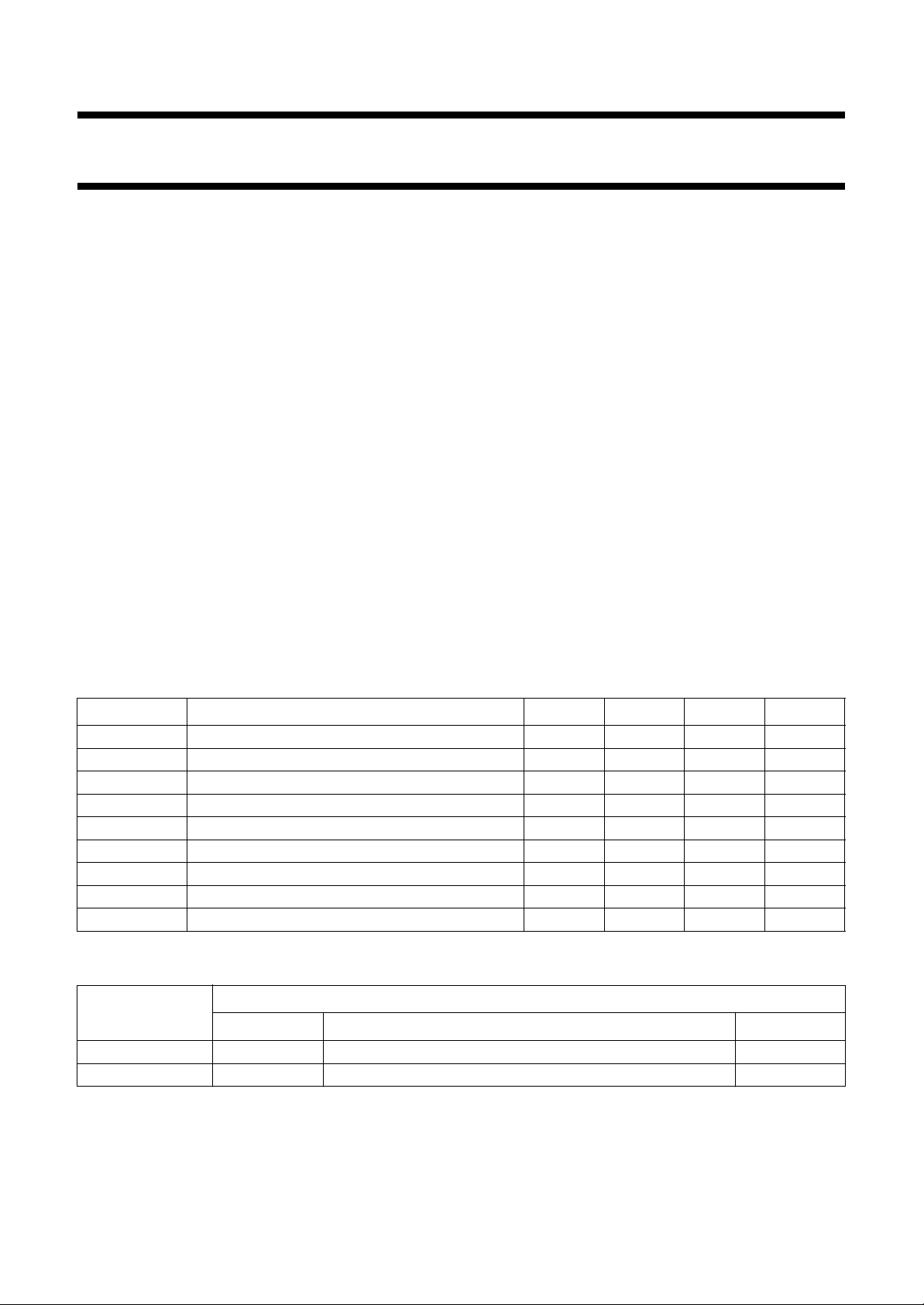
BLOCK DIAGRAM
V
V
SUB
EED
CCD
YOUT
18
MUX Y
6.7 MHz
LOW-PASS FILTER
MUX
SC LINE
MEMORIES
C1 C2 C3
SAA4981
(B-Y)OUT
17
MUX BY
6.7 MHz
LOW-PASS FILTER
MUX
SC LINE
MEMORIES
(R-Y)OUT
16
MUX RY
C1 C2 C3
6.7 MHz
LOW-PASS FILTER
MUX
SC LINE
MEMORIES
C1 C2 C3
3
CLAMP REFERENCE
MHA277
RYSIDE
BYSIDE
YSIDE
CLAOUT
BGREF
LMRY
C
LMBY
C
LMY
C
handbook, full pagewidth
V
V
EEA
CCA
20 19 8 7 4
SC LINE MEMORY
SC LINE MEMORY
5 MHz
LOW-PASS FILTER
CLAMP
23
YIN
SC LINE MEMORY
SC LINE MEMORY
5 MHz
LOW-PASS FILTER
CLAMP
22
(B-Y)IN
1995 Oct 05 3
SC LINE MEMORY
SC LINE MEMORY
5 MHz
LOW-PASS FILTER
CLAMP
21
(R-Y)IN
3
C1
HORIZONTAL
SEPARATION
6
HREF
C2
C3
CONTROLLER
PLL
54 MHz
Fig.1 Block diagram.
11 1 2 3 24 5 15 14 1310912
CTRL1 CTRL3
TEST CTRL2
Page 4
Philips Semiconductors Preliminary specification
Monolithic integrated 16 : 9 compressor SAA4981
PINNING
SYMBOL PIN DESCRIPTION
C
LMY
C
LMBY
C
LMRY
SUB 4 substrate connection (see Fig.5)
CLAOUT 5 internal clamping reference voltage
HREF 6 horizontal reference input
V
EED
V
CCD
CTRL1 9 control input 1
CTRL2 10 control input 2
CTRL3 11 control input 3
TEST 12 test mode activation
RYSIDE 13 side panel input for RY
BYSIDE 14 side panel input for BY
YSIDE 15 side panel input for Y
(R−Y)OUT 16 output signal for (R−Y)
(B−Y)OUT 17 output signal for (B−Y)
YOUT 18 output signal for Y
V
EEA
V
CCA
(R−Y)IN 21 input signal for (R−Y)
(B−Y)IN 22 input signal for (B−Y)
YIN 23 input signal for Y
BGREF 24 decoupling capacitor for internal
1 decoupling capacitor for Y
reference voltage
2 decoupling capacitor for BY
reference voltage
3 decoupling capacitor for RY
reference voltage
output
7 ground for digital section
8 positive digital supply voltage
19 ground for analog section
20 positive analog supply voltage
reference voltage
handbook, halfpage
1
C
LMY
LMBY
LMRY
SUB
HREF
2
3
4
5
6
C
C
CLAOUT
SAA4981
7
V
EED
8
V
CCD
TEST
9
10
11
12
CTRL1
CTRL2
CTRL3
Fig.2 Pin configuration.
MHA276
24
23
22
21
20
19
18
17
16
15
14
13
BGREF
YIN
(B-Y)IN
(R-Y)IN
V
CCA
V
EEA
YOUT
(B−Y)OUT
(R−Y)OUT
YSIDE
BYSIDE
RYSIDE
1995 Oct 05 4
Page 5

Philips Semiconductors Preliminary specification
Monolithic integrated 16 : 9 compressor SAA4981
FUNCTIONAL DESCRIPTION
Applicable video standards
The integrated 16 : 9 compressor can be used for the
following video standards; B, C, D, G, H, I, K, K1, L,
M and N. standards D, I, K, K1 and L will show a reduced
video bandwidth above 5 MHz.
Clamping circuit
The clamping circuits clamp the video input signals Y,
(B−Y) and (R−Y) to the DC level of the clamp reference
signal fed from the clamp reference circuit. This is
necessary to ensure that the input signals are in the
correct input voltage range for the 5 MHz low-pass filters
and the SC line memories.
Internal pre filters
Before the signals are sampled in the time discrete and
amplitude continuous area, low-pass filtering is necessary
to avoid any aliasing. Even if the inputs have already been
low-pass filtered further filtering is advantageous for the
electromagnetic compatibility (EMC). The same transfer
function is used for all three low-pass filters because of the
same bandwidth for the luminance and chrominance
signals (up to 5 MHz).
SC line memories
After the low-pass filters the input signals are fed to the SC
line memories. The signals are sampled at a clock
frequency of 13.5 MHz. One video line later the signals are
read with a clock frequency of 18 MHz in the compression
mode. The result of the different clock frequencies is a
4
horizontal compression by a factor of
⁄3. The clocks and
the horizontal starting pulses for the SC line memories are
fed from the controller.
Two line memories are required for each signal path
because in the compression mode, in one video line the
signals are sampled to the SC line memories with
13.5 MHz and one video line later the signals are read with
18 MHz. In the bypass mode, via the SC line memories, in
one video line the signals are sampled with 13.5 MHz and
one video line later the signals are read with 13.5 MHz.
The SC line memories are suitable for signals with a
bandwidth up to 5 MHz. With a multiplexer (MUX) behind
the SC line memories, the sampled video signal is
connected to the internal post filters.
Output multiplexer MUX Y, MUX (B−Y) and MUX (R−Y)
The output multiplexers are controlled via C1 and C2 fed
from the controller. The multiplexers are used to connect
one of the four input signals to the output and, also, enable
fast switching.
The input signals of the multiplexers for one component
[Y, (B−Y) or (R−Y)] are as follows:
• The output signal of the post filter
• The uncompressed signal after the input clamping
• The clamping reference signal
• The signal for the side panel determined by YSIDE,
BYSIDE and RYSIDE.
The horizontal separation circuit
The 54 MHz horizontal PLL is locked to the positive edge
of the digital HREF signal, which is generated in the
horizontal separation circuit. It is also possible to use the
positive edge of the burst key of a sandcastle signal.
54 MHz horizontal PLL
The 13.5 MHz clock frequency for the sampling clock and
the 18 MHz clock frequency for the reading clock are
generated in the 54 MHz horizontal PLL. The 13.5 MHz
clock and the 18 MHz clock are line locked.
Clamp reference
Reference voltages are generated In the clamp reference
block. These DC signals are used in the clamping circuits
as input signals for the output multiplexers and as
reference voltages for the SC line memories.
Four external capacitors at the pins C
LMY
, C
LMBY
, C
LMRY
and BGREF respectively are necessary to provide
smoothing for the reference voltages. A black level
reference signal is available at CLAOUT.
1995 Oct 05 5
Page 6
Philips Semiconductors Preliminary specification
Monolithic integrated 16 : 9 compressor SAA4981
Controller
The controller generates the clocks and the horizontal start
signals for the SC line memories and, also, the control
signals for the output multiplexers. The timing for the start
reading signal for three different screen positions (left,
centre and right) and the control signals for the
multiplexers (C1 and C2) is fixed. For the uncompressed
signals a bypass via the SC line memories and a bypass
not via the SC line memories is available. When the
signals do not pass the line memories, the frequency
response is not affected by the si-function. The
compression and bypass mode via the line memories is
delayed by one line with respect to the bypass mode not
via the line memory.
The 16 : 9 compressor is controlled via the control signals
CTRL1, CTRL2 and CTRL3 (see Table 1). The test input
must be LOW level.
Table 1 Functions of the control signals
CTRL1 CTRL2 CTRL3 FUNCTION
LOW LOW LOW bypass (through the line
memories)
LOW HIGH LOW compression, left position
HIGH LOW LOW compression, centre position
HIGH HIGH LOW compression, right position
LOW LOW HIGH bypass (not through the line
memories)
Signals for the side panels
The luminance and chrominance of the side panels is
determined by the external signals YSIDE, BYSIDE and
RYSIDE. This external generated side panel signal can be
referenced to the internal black level reference signal via
the output CLAOUT (pin 5).
Horizontal timing (see Fig.3)
The horizontal timing refers to the positive edge of the
input HREF signal.
The following timing parameters are valid for a horizontal
frequency of 15.625 kHz.
Input clamping typically starts at t
= 1.55 µs and ends at
A
tB= 3.78 µs.
Internal post filters
The output signals of the SC line memories have to be
filtered with three 6.7 MHz low-pass filters to eliminate the
high frequencies caused by the time discrete signal
processing. The cut-off frequency of 6.7 MHz is necessary
because, as a result of the
3
⁄4 compression factor, the
frequencies are shifted to a higher frequency band with the
inverse compression factor (e.g. 5 MHz→ compression→
6.67 MHz). Due to the common bandwidth requirements
for all three outputs of the SC line memories the same
transfer function for the filters can be used.
Remark: These filters do not provide an si-correction. This
means that an input signal with a frequency of 5 MHz will
be damped by 2.1 dB at the output if the signal passes an
SC line memory.
1995 Oct 05 6
Page 7

Philips Semiconductors Preliminary specification
Monolithic integrated 16 : 9 compressor SAA4981
handbook, full pagewidth
6.3 µs
HREF
1.5 µs
1.5 µs
49 µs (used for compression)
side
panel
side
panel
compressed video
(left position)
64 µs
sampled video
52 µs
36.75 µs
compressed video
(centre position)
(2)
(1)
side
panel
compressed video
(right position)
side
panel
(2)
bypassed video
(bypass via the Line Memories)
(2)
(2)
bypassed video
(full bypass not through the Line Memories)
(1) Nominal timing for a 52 µs active video signal to generate a centred compressed video signal.
(2) Worst case picture position for a 52 µs active video signal to generate no visible blanking between side panels and compressed video.
(1)
MHA278
Fig.3 Horizontal timing.
1995 Oct 05 7
Page 8

Philips Semiconductors Preliminary specification
Monolithic integrated 16 : 9 compressor SAA4981
handbook, full pagewidth
CVBS
Y/C
COLOUR DECODER
TDA4650 OR TDA4655/7
AND TDA4665
sync
TDA2579B
ASC
SYNC
Y
−(B−Y)
−(R−Y)
3 3 3
1
PICTURE
SIGNAL
IMPROVEMENT
TDA4670/1
sandcastle
Y
−(B−Y)
−(R−Y)
16:9
COMPRESSOR
SAA4981
31
CTRL SIDE
YOUT
−(B−Y)OUT
−(R−Y)OUT
VIDEO
PROCESSOR
TDA4680/7
TDA4780
13
MHA279
Fig.4 Receiver for 16 : 9, 50 Hz and 15.625 kHz with 16 : 9 compressor.
LIMITING VALUES
In accordance with the Absolute Maximum Rating System (IEC 134).
SYMBOL PARAMETER CONDITIONS MIN. MAX. UNIT
V
n
V
6
P
tot
T
stg
T
amb
V
es
voltage on any pin (except pin 6 HREF) V
input voltage at pin 6 −0.5 +6.5 V
total power dissipation − 0.5 W
storage temperature −25 +150 °C
operating ambient temperature −20 +70 °C
electrostatic handling for all pins note 1 −500 +500 V
V
EEA
EED
− 0.5 V
− 0.5 V
CCA
CCD
+ 0.5 V
+ 0.5 V
note 2 −4000 +4000 V
R
G
B
Notes
1. Equivalent to discharging a 200 pF capacitor via a 0 Ω series resistor.
2. Equivalent to discharging a 100 pF capacitor via a 1.5 kΩ series resistor.
QUALITY SPECIFICATION
In accordance with
UZW-B0/FQ-0601
. ESD classification A.
1995 Oct 05 8
Page 9

Philips Semiconductors Preliminary specification
Monolithic integrated 16 : 9 compressor SAA4981
CHARACTERISTICS
V
CCA=VCCD
connected to CLAOUT; all voltages are referenced to V
(CCIR recommended 471-1), Y = 0.32 V (p-p), (B−Y) = 1.33 V (p-p), (R−Y) = 1.05 V (p-p); source impedance
Zis= 300 Ω; coupling capacitor Ck= 2.2 nF; output loads connected to ground RL=1MΩ, CL= 20 pF; measured in
Fig.5; test input pin 12 has to be connected to V
SYMBOL PARAMETER CONDITIONS MIN. TYP. MAX. UNIT
Supply (pins 20, 19, 8, 7 and 4); note 1
V
CCA
I
CCA
V
CCD
I
CCD
Video inputs (pins 23, 22 and 21)
Y
V
iY(p-p)
C
I(Y)
I
LI(Y)
R
iY(cl)
(B−Y)
V
i(B-Y)(p-p)
C
I(B-Y)
I
LI(B-Y)
R
I(B-Y)(cl)
(R−Y)
V
i(R−Y)(p-p)
C
I(R−Y)
I
LI(R−Y)(cl)
R
I(R−Y)(cl)
HREF input (pin 6)
V
i(top)
I
LI(HREF)
C
I(HREF)
V
slice
f
i
t
W
S
HREF
Side panel inputs (pins 15, 14 and 13)
V
i(side)
C
I(side)
I
LI(side)
=5V; T
amb
=25°C; f
= 15.625 kHz; substrate connected to V
HREF
= 0 V; input signal EBU colour bar 100/0/75/0
EEA
; unless otherwise specified.
EED
; YSIDE, BYSIDE and RYSIDE are
EED
analog supply voltage 4.75 5.0 5.5 V
analog supply current 35 50 65 mA
digital supply voltage 4.75 5 5.5 V
digital supply current 1 9 14 mA
input voltage (peak-to-peak value) active video − 0.32 0.45 V
input capacitance −−10 pF
input leakage current between clamping −−0.1 µA
input resistance during clamping − 25kΩ
input voltage (peak-to-peak value) active video − 1.33 1.9 V
input capacitance −−10 pF
input leakage current between clamping −−0.1 µA
input resistance during clamping − 25kΩ
input voltage (peak-to-peak value) active video − 1.05 1.5 V
input capacitance −−10 pF
input leakage current between clamping −−0.1 µA
input resistance during clamping − 25kΩ
input voltage of the top pulse 3.0 − 6.5 V
input leakage current −−10 µA
input capacitance −−10 pF
slicing level below top pulse 0.5 0.75 1.0 V
input frequency 14.0 15.6 17.2 kHz
pulse width 1 −−µs
steepness 0.5 V under top 400 −−mV/ns
input voltage 0.5 − 2.5 V
input capacitance −−10 pF
input leakage current −−0.1 µA
1995 Oct 05 9
Page 10

Philips Semiconductors Preliminary specification
Monolithic integrated 16 : 9 compressor SAA4981
SYMBOL PARAMETER CONDITIONS MIN. TYP. MAX. UNIT
Control inputs/outputs (pins 9, 10 and 11)
V
IH
V
IL
C
Ictr
I
LIctr
Clamping reference output (pin 5)
V
o5
R
L
C
L
External capacitors (pins 1, 2 and 3)
C
DL
V
oCDL
External capacitor (pin 24)
C
BGREF
V
oBGREF
Video output signals (pins 18, 17 and 16)
HIGH level input voltage 3.5 −−V
LOW level input voltage −−1.5 V
input capacitance −−10 pF
input leakage current −−1µA
output voltage 1.3 1.45 1.6 V
load resistor 10 −−kΩ
load capacitor −−30 pF
value for capacitor − 100 − nF
output voltage 1.3 1.45 1.6 V
value for capacitor − 100 − nF
output voltage 1.1 1.25 1.4 V
YOUT
R
O(Y)
V
oY(p-p)
S/N signal-to-noise ratio 0.32 V (p-p)/V
output resistance −−100 Ω
output voltage (peak-to-peak value) − 0.32 0.5 V
noise;
eff
52 −−dB
unweighted;
fi= 200 kHz to 5 MHz
FPN(p-p) fixed pattern noise peak-to-peak
f
< 5 MHz 42 −−dB
clk
referenced to 0.32 V (p-p) video
α
ctY
| delay between different outputs −−30 ns
|t
d
t
d
crosstalk between different inputs fi= 1 MHz 40 −−dB
jitter in output signal referenced to
−−10 ns
HREF input signal
Bypass not via the SC line memories
G
Y1
G
Y2
frequency response f
= 0 to 4 MHz −0.5 − +0.5 dB
ripple
frequency response attenuation at 5 MHz
0 −−2dB
compared to 1 MHz
Bypass via the SC line memories;
G
Y3
G
Y4
G
Y5
G
Y6
G
Y7
YOUT/YIN at input frequency fi= 1 MHz −1.1 − +0.9 dB
YOUT/YIN at input frequency fi= 2 MHz −1.3 − +0.7 dB
YOUT/YIN at input frequency fi= 3 MHz −1.7 − +0.3 dB
YOUT/YIN at input frequency fi= 4 MHz −2.3 −−0.3 dB
YOUT/YIN at input frequency fi= 5 MHz −3.1 −−1.1 dB
note 2
1995 Oct 05 10
Page 11

Philips Semiconductors Preliminary specification
Monolithic integrated 16 : 9 compressor SAA4981
SYMBOL PARAMETER CONDITIONS MIN. TYP. MAX. UNIT
Compressed video;
G
Y8
G
Y9
G
Y10
G
Y11
G
Y12
G
Y13
A
Ypre
A
Ypost
note 2
YOUT/YIN at input frequency fi= 1 MHz; fo= 1.3 MHz −1 − +1 dB
YOUT/YIN at input frequency fi= 2 MHz; fo= 2.7 MHz −1 − +1 dB
YOUT/YIN at input frequency fi= 3 MHz; fo= 4 MHz −2 − 0dB
YOUT/YIN at input frequency fi= 3.75 MHz; fo= 5 MHz −3 −−1dB
YOUT/YIN at input frequency fi= 4 MHz; fo= 5.3 MHz −4 −−1dB
YOUT/YIN at input frequency fi= 5 MHz; fo= 6.67 MHz −6 −−1dB
pre filter stop-band characteristic,
damping factor for input signals
post filter stop-band characteristic,
damping factor for input signals
fi> 10 MHz 20 −−dB
> 20 MHz 32 −−dB
f
i
> 100 MHz 42 −−dB
f
i
fi> 14 MHz 20 −−dB
> 20 MHz 32 −−dB
f
i
> 100 MHz 40 −−dB
f
i
(B−Y)OUT
R
O(U)
V
oU(p-p)
S/N signal-to-noise ratio 1.33 V (p-p)/V
output resistance −−100 Ω
output voltage (peak-to-peak value) − 1.33 2.1 V
noise;
eff
54 −−dB
unweighted;
fi= 200 kHz to 5 MHz
FPN(p-p) fixed pattern noise peak-to-peak
< 5 MHz 42 −−dB
f
clk
referenced to 1.33 V (p-p) video
α
ctU
| delay between different outputs −−30 ns
|t
d
t
d
crosstalk between different inputs fi= 1 MHz 40 −−dB
jitter in output signal to input HREF
−−10 ns
signal
Bypass not via the SC line memories
G
U1
G
U2
frequency response f
= 0 to 4 MHz −0.5 − +0.5 dB
ripple
frequency response attenuation at 5 MHz
0 −−2dB
compared to 1 MHz
Bypass via the SC line memories;
G
U3
G
U4
G
U5
G
U6
G
U7
(B−Y)OUT/(B−Y)IN at input frequency fi= 1 MHz −1.1 − +0.9 dB
(B−Y)OUT/(B−Y)IN at input frequency fi= 2 MHz −1.3 − +0.7 dB
(B−Y)OUT/(B−Y)IN at input frequency fi= 3 MHz −1.7 − +0.3 dB
(B−Y)OUT/(B−Y)IN at input frequency fi= 4 MHz −2.3 −−0.3 dB
(B−Y)OUT/(B−Y)IN at input frequency fi= 5 MHz −3.1 −−1.1 dB
note 2
1995 Oct 05 11
Page 12

Philips Semiconductors Preliminary specification
Monolithic integrated 16 : 9 compressor SAA4981
SYMBOL PARAMETER CONDITIONS MIN. TYP. MAX. UNIT
Compressed video;
G
U8
G
U9
G
U10
G
U11
G
U12
G
U13
A
Upre
A
Upost
note 2
(B−Y)OUT/(B−Y)IN at input frequency fi= 1 MHz; fo= 1.3 MHz −1 − +1 dB
(B−Y)OUT/(B−Y)IN at input frequency fi= 2 MHz; fo= 2.7 MHz −1 − +1 dB
(B−Y)OUT/(B−Y)IN at input frequency fi= 3 MHz; fo= 4 MHz −2 − 0dB
(B−Y)OUT/(B−Y)IN at input frequency fi= 3.75 MHz; fo= 5 MHz −3 −−1dB
(B−Y)OUT/(B−Y)IN at input frequency fi= 4 MHz; fo= 5.3 MHz −4 −−1dB
(B−Y)OUT/(B−Y)IN at input frequency fi= 5 MHz; fo= 6.67 MHz −6 −−1dB
pre filter stop-band characteristic,
damping factor for input signals
post filter stop-band characteristic,
damping factor for input signals
fi> 10 MHz 20 −−dB
> 20 MHz 32 −−dB
f
i
> 100 MHz 42 −−dB
f
i
fi> 14 MHz 20 −−dB
> 20 MHz 32 −−dB
f
i
> 100 MHz 40 −−dB
f
i
(R−Y)OUT
R
O(V)
V
oV
S/N signal-to-noise ratio 1.05 V (p-p)/V
output resistance −−100 Ω
output voltage (peak-to-peak value) − 1.05 1.7 V
noise;
eff
52 −−dB
unweighted;
fi= 200 kHz to 5 MHz
FPN(p-p) fixed pattern noise peak-to-peak
< 5 MHz 40 −−dB
f
clock
referenced to 1.05 V (p-p) video
α
ctV
| delay between different outputs −−30 ns
|t
d
t
d
crosstalk between different inputs fi= 1 MHz 40 −−dB
jitter in output signal to input HREF
−−10 ns
signal
Bypass not via the SC line memories
G
V1
G
V2
frequency response f
= 0 to 4 MHz −0.5 − +0.5 dB
ripple
frequency response attenuation at 5 MHz
0 −−2dB
compared to 1 MHz
Bypass via the SC line memories;
G
V3
G
V4
G
V5
G
V6
G
V7
(R−Y)OUT/(R−Y)IN at input frequency fi= 1 MHz −1.1 − +0.9 dB
(R−Y)OUT/(R−Y)IN at input frequency fi= 2 MHz −1.3 − +0.7 dB
(R−Y)OUT/(R−Y)IN at input frequency fi= 3 MHz −1.7 − +0.3 dB
(R−Y)OUT/(R−Y)IN at input frequency fi= 4 MHz −2.3 −−0.3 dB
(R−Y)OUT/(R−Y)IN at input frequency fi= 5 MHz −3.1 −−1.1 dB
note 2
1995 Oct 05 12
Page 13

Philips Semiconductors Preliminary specification
Monolithic integrated 16 : 9 compressor SAA4981
SYMBOL PARAMETER CONDITIONS MIN. TYP. MAX. UNIT
Compressed video;
G
V8
G
V9
G
V10
G
V11
G
V12
G
V13
A
Vpre
A
Vpost
note 2
(R−Y)OUT/(R−Y)IN at input frequency fi= 1 MHz; fo= 1.3 MHz −1 − +1 dB
(R−Y)OUT/(R−Y)IN at input frequency fi= 2 MHz; fo= 2.7 MHz −1 − +1 dB
(R−Y)OUT/(R−Y)IN at input frequency fi= 3 MHz; fo= 4 MHz −2 − 0dB
(R−Y)OUT/(R−Y)IN at input frequency fi= 3.75 MHz; fo= 5 MHz −3 −−1dB
(R−Y)OUT/(R−Y)IN at input frequency fi= 4 MHz; fo= 5.3 MHz −4 −−1dB
(R−Y)OUT/(R−Y)IN at input frequency fi= 5 MHz; fo= 6.67 MHz −6 −−1dB
pre filter stop-band characteristic,
damping factor for input signals
post filter stop-band characteristic,
damping factor for input signals
fi> 10 MHz 20 −−dB
> 20 MHz 32 −−dB
f
i
> 100 MHz 42 −−dB
f
i
fi> 14 MHz 20 −−dB
> 20 MHz 32 −−dB
f
i
> 100 MHz 40 −−dB
f
i
Video outputs YOUT, (B−Y)OUT and (R−Y)OUT
R
ATIO OF OUTPUT AMPLITUDES FOR EQUAL INPUT SIGNALS FOR Y, (B−Y) AND (R−Y)
V
oY/VoU
V
oY/VoV
V
oU/VoV
YOUT/(B−Y)OUT VI= 0.32 V (p-p); fi≤ 1 MHz −0.4 − +0.4 dB
YOUT/(R−Y)OUT VI= 0.32 V (p-p); fi≤ 1 MHz −0.4 − +0.4 dB
(B−Y)OUT/(R−Y)OUT VI= 1.33 V (p-p) −0.4 − +0.4 dB
Notes
1. ∆V1= V
CCA
− V
≤300 mV; ∆V2= V
CCD
EED
− V
≤300 mV with V
EEA
= SUB (latch-up prevention).
EED
2. This frequency response includes the si-attenuation as a result of the time discrete signal processing. An
si-correction is not performed.
1995 Oct 05 13
Page 14

Philips Semiconductors Preliminary specification
Monolithic integrated 16 : 9 compressor SAA4981
APPLICATION INFORMATION
ok, full pagewidth
+ 5 V
47 µF
ferrit
pearl
video signal
2.2
nF
inputs
V
EEA
100
2.2
nF
nF
24 23 22 21 20 19 18 17 16 15 14 13
2.2
nF
2.2 Ω
10 nF
47 µF
10 nF
47 µF
10 nF
V
EEA
video signal
outputs
CLAOUT
SAA4981
1234567 89101112
100nF100
100
nF
V
EEAVEEAVEEA
(2)
nF
V
EED
clamp reference
voltage output
V
EED
line reference
input
V
10 nF
10 nF
47 µF
EEA
+ 5 V
2.2
Ω
5.6 Ω15 Ω
ferrit
pearl
control inputs
see Table 1
MHA280
(1)
V
EED
(1) Connected to CLAOUT for black side panels.
(2) Substrate (pin 4) has to be connected to V
EED
. V
EEA
and V
. Substrates have to be separated as much as possible.
EED
Fig.5 Application diagram.
1995 Oct 05 14
Page 15

Philips Semiconductors Preliminary specification
Monolithic integrated 16 : 9 compressor SAA4981
PACKAGE OUTLINES
DIP24: plastic dual in-line package; 24 leads (600 mil)
D
seating plane
L
Z
24
pin 1 index
e
b
SOT101-1
M
E
A
2
A
A
1
w M
b
1
13
E
c
(e )
1
M
H
1
0 5 10 mm
scale
DIMENSIONS (inch dimensions are derived from the original mm dimensions)
A
A
A
UNIT
inches
Note
1. Plastic or metal protrusions of 0.25 mm maximum per side are not included.
max.
mm
OUTLINE
VERSION
SOT101-1
1 2
min.
max.
1.7
1.3
0.066
0.051
IEC JEDEC EIAJ
051G02 MO-015AD
b
b
1
0.53
0.38
0.021
0.015
0.32
0.23
0.013
0.009
REFERENCES
cD E e M
32.0
31.4
1.26
1.24
1995 Oct 05 15
12
14.1
13.7
0.56
0.54
(1)(1)
e
L
3.9
3.4
EUROPEAN
PROJECTION
M
15.80
15.24
0.62
0.60
E
17.15
15.90
0.68
0.63
1
0.15
0.13
H
ISSUE DATE
w
0.252.54 15.24
0.010.10 0.60
92-11-17
95-01-23
Z
max.
2.25.1 0.51 4.0
0.0870.20 0.020 0.16
(1)
Page 16

Philips Semiconductors Preliminary specification
Monolithic integrated 16 : 9 compressor SAA4981
SO24: plastic small outline package; 24 leads; body width 7.5 mm
D
c
y
Z
24
pin 1 index
1
e
13
12
w
b
p
M
SOT137-1
E
H
E
Q
A
2
A
1
L
p
L
detail X
(A )
A
X
v
M
A
A
3
θ
0 5 10 mm
scale
DIMENSIONS (inch dimensions are derived from the original mm dimensions)
UNIT
mm
inches
A
max.
2.65
0.10
A1A2A
0.30
2.45
0.10
2.25
0.012
0.096
0.004
0.089
0.25
0.01
b
3
p
0.49
0.32
0.36
0.23
0.019
0.013
0.014
0.009
(1)E(1) (1)
cD
15.6
7.6
7.4
0.30
0.29
1.27
0.050
15.2
0.61
0.60
Note
1. Plastic or metal protrusions of 0.15 mm maximum per side are not included.
OUTLINE
VERSION
SOT137-1
IEC JEDEC EIAJ
075E05 MS-013AD
REFERENCES
1995 Oct 05 16
eHELLpQ
10.65
10.00
0.42
0.39
1.4
0.055
1.1
0.4
0.043
0.016
1.1
1.0
0.043
0.039
PROJECTION
0.25
0.25 0.1
0.01
0.01
EUROPEAN
ywv θ
Z
0.9
0.4
0.035
0.004
0.016
ISSUE DATE
92-11-17
95-01-24
o
8
o
0
Page 17

Philips Semiconductors Preliminary specification
Monolithic integrated 16 : 9 compressor SAA4981
SOLDERING
Introduction
There is no soldering method that is ideal for all IC
packages. Wave soldering is often preferred when
through-hole and surface mounted components are mixed
on one printed-circuit board. However, wave soldering is
not always suitable for surface mounted ICs, or for
printed-circuits with high population densities. In these
situations reflow soldering is often used.
This text gives a very brief insight to a complex technology.
A more in-depth account of soldering ICs can be found in
our
“IC Package Databook”
(order code 9398 652 90011).
DIP
OLDERING BY DIPPING OR BY WA VE
S
The maximum permissible temperature of the solder is
260 °C; solder at this temperature must not be in contact
with the joint for more than 5 seconds. The total contact
time of successive solder waves must not exceed
5 seconds.
The device may be mounted up to the seating plane, but
the temperature of the plastic body must not exceed the
specified maximum storage temperature (T
stg max
). If the
printed-circuit board has been pre-heated, forced cooling
may be necessary immediately after soldering to keep the
temperature within the permissible limit.
EPAIRING SOLDERED JOINTS
R
Apply a low voltage soldering iron (less than 24 V) to the
lead(s) of the package, below the seating plane or not
more than 2 mm above it. If the temperature of the
soldering iron bit is less than 300 °C it may remain in
contact for up to 10 seconds. If the bit temperature is
between 300 and 400 °C, contact may be up to 5 seconds.
SO
REFLOW SOLDERING
Reflow soldering techniques are suitable for all SO
packages.
Several techniques exist for reflowing; for example,
thermal conduction by heated belt. Dwell times vary
between 50 and 300 seconds depending on heating
method. Typical reflow temperatures range from
215 to 250 °C.
Preheating is necessary to dry the paste and evaporate
the binding agent. Preheating duration: 45 minutes at
45 °C.
AVE SOLDERING
W
Wave soldering techniques can be used for all SO
packages if the following conditions are observed:
• A double-wave (a turbulent wave with high upward
pressure followed by a smooth laminar wave) soldering
technique should be used.
• The longitudinal axis of the package footprint must be
parallel to the solder flow.
• The package footprint must incorporate solder thieves at
the downstream end.
During placement and before soldering, the package must
be fixed with a droplet of adhesive. The adhesive can be
applied by screen printing, pin transfer or syringe
dispensing. The package can be soldered after the
adhesive is cured.
Maximum permissible solder temperature is 260 °C, and
maximum duration of package immersion in solder is
10 seconds, if cooled to less than 150 °C within
6 seconds. Typical dwell time is 4 seconds at 250 °C.
A mildly-activated flux will eliminate the need for removal
of corrosive residues in most applications.
EPAIRING SOLDERED JOINTS
R
Fix the component by first soldering two diagonally-
opposite end leads. Use only a low voltage soldering iron
(less than 24 V) applied to the flat part of the lead. Contact
time must be limited to 10 seconds at up to 300 °C. When
using a dedicated tool, all other leads can be soldered in
one operation within 2 to 5 seconds between
270 and 320 °C.
Reflow soldering requires solder paste (a suspension of
fine solder particles, flux and binding agent) to be applied
to the printed-circuit board by screen printing, stencilling or
pressure-syringe dispensing before package placement.
1995 Oct 05 17
Page 18

Philips Semiconductors Preliminary specification
Monolithic integrated 16 : 9 compressor SAA4981
DEFINITIONS
Data sheet status
Objective specification This data sheet contains target or goal specifications for product development.
Preliminary specification This data sheet contains preliminary data; supplementary data may be published later.
Product specification This data sheet contains final product specifications.
Limiting values
Limiting values given are in accordance with the Absolute Maximum Rating System (IEC 134). Stress above one or
more of the limiting values may cause permanent damage to the device. These are stress ratings only and operation
of the device at these or at any other conditions above those given in the Characteristics sections of the specification
is not implied. Exposure to limiting values for extended periods may affect device reliability.
Application information
Where application information is given, it is advisory and does not form part of the specification.
LIFE SUPPORT APPLICATIONS
These products are not designed for use in life support appliances, devices, or systems where malfunction of these
products can reasonably be expected to result in personal injury. Philips customers using or selling these products for
use in such applications do so at their own risk and agree to fully indemnify Philips for any damages resulting from such
improper use or sale.
1995 Oct 05 18
Page 19

Philips Semiconductors Preliminary specification
Monolithic integrated 16 : 9 compressor SAA4981
NOTES
1995 Oct 05 19
Page 20

Philips Semiconductors – a worldwide company
Argentina: IEROD, Av. Juramento 1992 - 14.b, (1428)
BUENOS AIRES, Tel. (541)786 7633, Fax. (541)786 9367
Australia: 34 Waterloo Road, NORTH RYDE, NSW 2113,
Tel. (02)805 4455, Fax. (02)805 4466
Austria: Triester Str. 64, A-1101 WIEN, P.O. Box 213,
Tel. (01)60 101-1236, Fax. (01)60 101-1211
Belgium: Postbus 90050, 5600 PB EINDHOVEN, The Netherlands,
Tel. (31)40-2783749, Fax. (31)40-2788399
Brazil: Rua do Rocio 220 - 5
CEP: 04552-903-SÃO PAULO-SP, Brazil.
P.O. Box 7383 (01064-970),
Tel. (011)821-2333, Fax. (011)829-1849
Canada: PHILIPS SEMICONDUCTORS/COMPONENTS:
Tel. (800) 234-7381, Fax. (708) 296-8556
Chile: Av. Santa Maria 0760, SANTIAGO,
Tel. (02)773 816, Fax. (02)777 6730
China/Hong Kong: 501 Hong Kong Industrial Technology Centre,
72 Tat Chee Avenue, Kowloon Tong, HONG KONG,
Tel. (852)2319 7888, Fax. (852)2319 7700
Colombia: IPRELENSO LTDA, Carrera 21 No. 56-17,
77621 BOGOTA, Tel. (571)249 7624/(571)217 4609,
Fax. (571)217 4549
Denmark: Prags Boulevard 80, PB 1919, DK-2300
COPENHAGEN S, Tel. (032)88 2636, Fax. (031)57 1949
Finland: Sinikalliontie 3, FIN-02630 ESPOO,
Tel. (358)0-615 800, Fax. (358)0-61580 920
France: 4 Rue du Port-aux-Vins, BP317,
92156 SURESNES Cedex,
Tel. (01)4099 6161, Fax. (01)4099 6427
Germany: P.O. Box 10 63 23, 20043 HAMBURG,
Tel. (040)3296-0, Fax. (040)3296 213.
Greece: No. 15, 25th March Street, GR 17778 TAVROS,
Tel. (01)4894 339/4894 911, Fax. (01)4814 240
India: Philips INDIA Ltd, Shivsagar Estate, A Block,
Dr. Annie Besant Rd. Worli, Bombay 400 018
Tel. (022)4938 541, Fax. (022)4938 722
Indonesia: Philips House, Jalan H.R. Rasuna Said Kav. 3-4,
P.O. Box 4252, JAKARTA 12950,
Tel. (021)5201 122, Fax. (021)5205 189
Ireland: Newstead, Clonskeagh, DUBLIN 14,
Tel. (01)7640 000, Fax. (01)7640 200
Italy: PHILIPS SEMICONDUCTORS S.r.l.,
Piazza IV Novembre 3, 20124 MILANO,
Tel. (0039)2 6752 2531, Fax. (0039)2 6752 2557
Japan: Philips Bldg13-37, Kohnan 2-chome, Minato-ku, TOKYO 108,
Tel. (03)3740 5130, Fax. (03)3740 5077
Korea: Philips House, 260-199 Itaewon-dong,
Yongsan-ku, SEOUL, Tel. (02)709-1412, Fax. (02)709-1415
Malaysia: No. 76 Jalan Universiti, 46200 PETALING JAYA,
SELANGOR, Tel. (03)750 5214, Fax. (03)757 4880
Mexico: 5900 Gateway East, Suite 200, EL PASO, TX 79905,
Tel. 9-5(800)234-7381, Fax. (708)296-8556
th
floor, Suite 51,
Netherlands: Postbus 90050, 5600 PB EINDHOVEN, Bldg. VB,
Tel. (040)2783749, Fax. (040)2788399
New Zealand: 2 Wagener Place, C.P.O. Box 1041, AUCKLAND,
Tel. (09)849-4160, Fax. (09)849-7811
Norway: Box 1, Manglerud 0612, OSLO,
Tel. (022)74 8000, Fax. (022)74 8341
Pakistan: Philips Electrical Industries of Pakistan Ltd.,
Exchange Bldg. ST-2/A, Block 9, KDA Scheme 5, Clifton,
KARACHI 75600, Tel. (021)587 4641-49,
Fax. (021)577035/5874546
Philippines: PHILIPS SEMICONDUCTORS PHILIPPINES Inc,
106 Valero St. Salcedo Village, P.O. Box 2108 MCC, MAKATI,
Metro MANILA, Tel. (63) 2 816 6380, Fax. (63) 2 817 3474
Portugal: PHILIPS PORTUGUESA, S.A.,
Rua dr. António Loureiro Borges 5, Arquiparque - Miraflores,
Apartado 300, 2795 LINDA-A-VELHA,
Tel. (01)4163160/4163333, Fax. (01)4163174/4163366
Singapore: Lorong 1, Toa Payoh, SINGAPORE 1231,
Tel. (65)350 2000, Fax. (65)251 6500
South Africa: S.A. PHILIPS Pty Ltd.,
195-215 Main Road Martindale, 2092 JOHANNESBURG,
P.O. Box 7430, Johannesburg 2000,
Tel. (011)470-5911, Fax. (011)470-5494
Spain: Balmes 22, 08007 BARCELONA,
Tel. (03)301 6312, Fax. (03)301 42 43
Sweden: Kottbygatan 7, Akalla. S-164 85 STOCKHOLM,
Tel. (0)8-632 2000, Fax. (0)8-632 2745
Switzerland: Allmendstrasse 140, CH-8027 ZÜRICH,
Tel. (01)488 2211, Fax. (01)481 77 30
Taiwan: PHILIPS TAIWAN Ltd., 23-30F, 66, Chung Hsiao West
Road, Sec. 1. Taipeh, Taiwan ROC, P.O. Box 22978,
TAIPEI 100, Tel. (886) 2 382 4443, Fax. (886) 2 382 4444
Thailand: PHILIPS ELECTRONICS (THAILAND) Ltd.,
209/2 Sanpavuth-Bangna Road Prakanong,
Bangkok 10260, THAILAND,
Tel. (66) 2 745-4090, Fax. (66) 2 398-0793
Turkey:Talatpasa Cad. No. 5, 80640 GÜLTEPE/ISTANBUL,
Tel. (0212)279 27 70, Fax. (0212)282 67 07
United Kingdom: Philips Semiconductors LTD.,
276 Bath Road, Hayes, MIDDLESEX UB3 5BX,
Tel. (0181)730-5000, Fax. (0181)754-8421
United States:811 East Arques Avenue, SUNNYVALE,
CA 94088-3409, Tel. (800)234-7381, Fax. (708)296-8556
Uruguay: Coronel Mora 433, MONTEVIDEO,
Tel. (02)70-4044, Fax. (02)92 0601
Internet: http://www.semiconductors.philips.com/ps/
For all other countries apply to: Philips Semiconductors,
International Marketing and Sales, Building BE-p,
P.O. Box 218, 5600 MD EINDHOVEN, The Netherlands,
Telex 35000 phtcnl, Fax. +31-40-2724825
SCD44 © Philips Electronics N.V. 1995 Oct 05
All rights are reserved. Reproduction in whole or in part is prohibited without the
prior written consent of the copyright owner.
The information presented in this document does not form part of any quotation
or contract, is believed to be accurate and reliable and may be changed without
notice. No liability will be accepted by the publisher for any consequence of its
use. Publication thereof does not convey nor imply any license under patent- or
other industrial or intellectual property rights.
Printed in The Netherlands
533061/1500/02/pp20 Date of release: 1995 Oct 05
Document order number: 9397 750 00346
 Loading...