

Page 1

INTEGRATED CIRCUITS
DATA SH EET
SAA4978H
Picture Improved Combined
Network (PICNIC)
Product specification
Supersedes data of 1998 Oct 07
File under Integrated Circuits, IC02
1999 May 03
Page 2

Philips Semiconductors Product specification
Picture Improved Combined Network
(PICNIC)
CONTENTS
1 FEATURES
2 GENERAL DESCRIPTION
3 QUICK REFERENCE DATA
4 ORDERING INFORMATION
5 BLOCK DIAGRAM
6 PINNING INFORMATION
7 FUNCTIONAL DESCRIPTION
7.1 Analog input blocks
7.1.1 Gain elements for automatic gain control (9 dB
range)
7.1.2 Clamp circuit, clamping Y to digital level 32 and
UV to 0 (2’s complement)
7.1.3 Analog anti-aliasing prefilter
7.1.4 9-bit analog-to-digital conversion
7.2 Digital processing blocks
7.2.1 Overflow detection
7.2.2 Y delay
7.2.3 Transient noise suppression
7.2.4 Non-linear phase filter after ADC
7.2.5 4 MHz notch
7.2.6 Digital clamp correction for UV
7.2.7 4:4:4 downsampled to4:2:2 or4:1:1
7.2.8 Bus A format: interface formatting, timed with
enabling signal (see Table 1 and Fig.9)
7.2.9 Bus B format (see Table 1 and Fig.9)
7.2.10 Time base correction and sample rate
conversion
7.2.11 Noise reduction
7.2.12 Histogram
7.2.13 Subtitle detection
7.2.14 Black bar detection
7.2.15 Bus C format (see Table 1)
7.2.16 Bus D reformatter: the various input formats
are all converted to the internal 9 bits 4 :2:2
(see Table 1)
7.2.17 Peaking
7.2.18 Non-linear phase filter before DAC
7.2.19 DCTI
7.2.20 Border blank
7.3 Analog output blocks
7.3.1 Triple 10-bit digital-to-analog conversion
7.3.2 Analog anti-aliasing post-filter
7.3.3 PLL
7.3.4 SNERT
7.3.5 PSP
7.3.6 Microcontroller
7.3.7 Board level testability
7.3.8 Power-on reset
SAA4978H
8 CONTROL REGISTER DESCRIPTION
9 LIMITING VALUES
10 THERMAL CHARACTERISTICS
11 CHARACTERISTICS
12 APPLICATION
13 PACKAGE OUTLINE
14 SOLDERING
14.1 Introduction
14.2 Reflow soldering
14.3 Wave soldering
14.4 Repairing soldered joints
15 DEFINITIONS
16 LIFE SUPPORT APPLICATIONS
17 PURCHASE OF PHILIPS I2C COMPONENTS
1999 May 03 2
Page 3
Philips Semiconductors Product specification
Picture Improved Combined Network
(PICNIC)
1 FEATURES
• Clamp
• Analog AGC
• Triple YUV 9-bit Analog-to-Digital Converter (ADC)
• Triple bypassable analog anti-alias filter
• 4 MHz notch filter
• Non-linear phase filter after ADC
• 4:1:1 or 4:2:2 digital processing
• 4:1:1 or 4:2:2 selectable I/O interface
• Asynchronous digital input
• Time base correction
• Histogram analysis
• Histogram modification
• Subtitle detection
• Black bar detection
• Line memory based noise reduction (spatial)
• Noise level measurement
• Clamp noise reduction
• Dynamic peaking
• Energy measurement
• Multi Picture-In-Picture (multi PIP) decimation
• Differential Pulse Code Modulation (DPCM) data
decompression for colour
SAA4978H
• 2D-peaking and coring
• Non-linear phase filter before DAC
• Coaxial Transceiver Interface (CTI)
• Triple 10-bit Digital-to-Analog Converter (DAC)
• Triple bypassable analog reconstruction filter
• Embedded microcontroller (80C51 core)
• Programmable signal positioner
• SNERT interface
2
• I
C-bus user control interface
• Boundary Scan Test (BST).
2 GENERAL DESCRIPTION
The SAA4978H is a monolithic integrated circuit suitable
either for 1f
of picture improvement functions. It combines
analog-to-digital and digital-to-analog conversion for YUV
signals, digital processing, line-locked clock regeneration
and an 80C51 microcontroller core in one IC.
or 2fH applications that contain a large variety
H
3 QUICK REFERENCE DATA
SYMBOL PARAMETER CONDITIONS MIN. TYP. MAX. UNIT
V
V
I
DDA
I
DDD
f
clk
DDA
DDD
analog supply voltage 3.15 3.3 3.45 V
digital supply voltage 3.0 3.3 3.6 V
analog supply current V
digital supply current V
= 3.45 V − 145 180 mA
DDA
= 3.6 V − 210 270 mA
DDD
clock frequency − 16 − MHz
S/N signal-to-noise ratio default settings 50 −−dB
4 ORDERING INFORMATION
TYPE
NUMBER
NAME DESCRIPTION VERSION
SAA4978H QFP160 plastic quad flat package; 160 leads (lead length 1.6 mm);
PACKAGE
SOT322-2
body 28 × 28 × 3.4 mm; high stand-off height
1999 May 03 3
Page 4
This text is here in white to force landscape pages to be rotated correctly when browsing through the pdf in the Acrobat reader.This text is here in
o
_white to force landscape pages to be rotated correctly when browsing through the pdf in the Acrobat reader.This text is here inThis text is here in
white to force landscape pages to be rotated correctly when browsing through the pdf in the Acrobat reader. white to force landscape pages to be ...
1999 May 03 4
k, full pagewidth
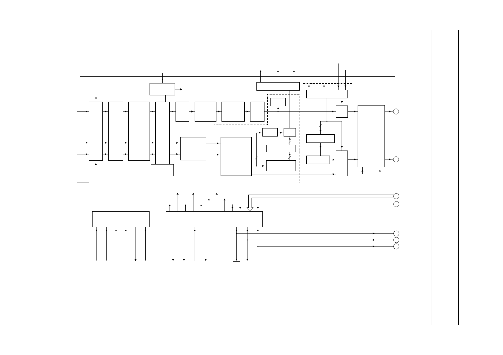
5 BLOCK DIAGRAM
Picture Improved Combined Network
(PICNIC)
Philips Semiconductors Product specification
V
DDA1
V
SSA1
DIFFIN
YIN
UIN
VIN
V
DDA4
V
SSA4
to
to
21
23
CLAMP
25
26
CLP
11, 22, 24, 31
13, 16, 27, 32
V
DDD1
V
DDD4
64, 87,
100, 135
to
V
SSD1
V
64, 90,
134, 139
TRIPLE
AGC
9-BIT
SAA4978H
to
SSD4
TRIPLE
ANALOG
PREFILTER
BGEXT
17
BAND GAP
REFERENCES
Ref L
Ref H
ADC
TRIPLE
9-BIT
OVERFLOW
DETECTOR
CLP
various
bias controls
Y
DELAY
CORRECTION
RED
WEC
UV
CLAMP
WEA
MAJORITY
FOLLOWER
FILTER
BLANKING
BORDER
IEC
PIXREP
PSPBST/TEST
NON-LINEAR
PHASE
FILTER
DOWNSAMPLER
HA
HREF
YA0
to
DITHER
11
DOWNSAMPLER
YA8
3-STATE
DITHER
MUX
FORMATTER
DITHER
WEA
4 MHz
NOTCH
bus A bus B
to
UVA8
5
10
to
UVB8
SYNCHRONIZE
REFORMATTER
UPSAMPLER
UVB0
UVA0
YB0
YB8
5
WEB
to
CLKAS
MUX
MUX
856675 to 6784 to 7643 to 5153 to 6162
TIME BASE
CORRECTION/
CONVERTER
SKEWEN SKEW
SAMPLE
RATE
A
B
C
D
41
40
39
38
37
36
TCK
TDO
TDI
TMS
TRST
TEST
HDFL
Standard bus width in data path is 9 bits; exceptions are marked.
10
157
INT1
158
INT0
FBL
30
29
19
18
HREFEXT
VA
VDFL
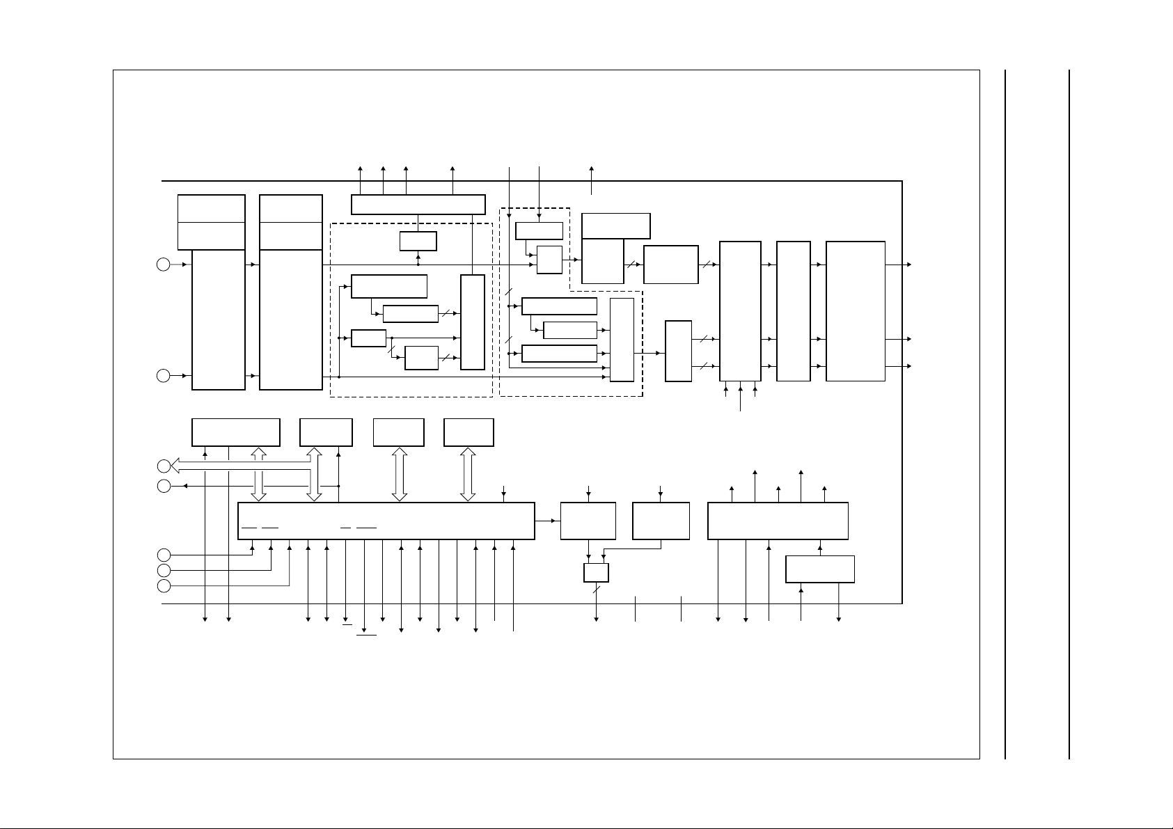
Fig.1 Block diagram (continued in Fig.2).
E
F
G
MHB172
SAA4978H
Page 5
This text is here in white to force landscape pages to be rotated correctly when browsing through the pdf in the Acrobat reader.This text is here in
b
_white to force landscape pages to be rotated correctly when browsing through the pdf in the Acrobat reader.This text is here inThis text is here in
white to force landscape pages to be rotated correctly when browsing through the pdf in the Acrobat reader. white to force landscape pages to be ...
1999 May 03 5
ook, full pagewidth
Philips Semiconductors Product specification
Picture Improved Combined Network
(PICNIC)
SPECTRAL
MEASUREMENT
ESTIMATION
A
B
C
D
E
F
G
SNDA
NOISE
NOISE
REDUCTION
SPECIAL FUNCTION
REGISTERS
INT1 INT0 P1.4
2
1
SNCL
SUBTITLE
DETECTION
BLACK BAR
DETECTION
HISTOGRAM
MODIFICATION
VARIOUS
REGISTERS
P2.7
to
P2.0
140
to
147
P0.7
to
P0.0
149
to
156
P1.1
YC8
to
WEC
DITHER
DATA8
EA PSEN
EA
YC0
IEC
112
3-STATE
DITHER
DOWNSAMPLER
DITHER
FORMATTER
8
DPCM
CODER
bus C
AUXILIARY
RAM
80C51 MICROCONTROLLER CORE
P3.5
P3.4 P1.2
137136
160138
159
ALE
T0
T1
PSEN
RSTW
UVC8
to
UVC0
5
4
PROGRAM
P1.3 P1.7
8
RSTR
MUX
ROM
SDA
YD0
UVD0
to
to
YD8
UVD8
91
to 99
UNDITHER
5
4
REFORMATTER
DPCM DECODER
101 to 109 110124 to 132114 to 122113
MUX
UPSAMPLER
bus D
RED
SPECTRAL
MEASUREMENT
DYNAMIC
10
PEAKING
MUX
NON-LINEAR
PHASE
FILTER
DCTI
10
10
10
PIXREP
BORDER
BLANK
BLANKING
BORDER
DAC
TRIPLE
10-BIT
TRIPLE
ANALOG
POST-FILTER
12
YOUT
14
UOUT
15
VOUT
SAA4978H
SKEWEN
CL16
bone
P1.5
P1.6
RST
64
59
SCL
RST
WATCHDOG
OR
WDRST V
7
FREQUENCY
42, 63, 86,
111, 133, 3
SSO1
to
V
SSO6
GUARD
52, 123, 148
V
DDO1
V
DDO3
89
88
CLK16
to
CLK32
SKEW
HA
PLL
28
CL16
CL32HREFCL16 CL16
CRYSTAL
OSCILLATOR
34
OSCI
35
MHB173
OSCO
SAA4978H
Standard bus width in data path is 9 bits; exceptions are marked.
Fig.2 Block diagram (continued from Fig.1).
Page 6

Philips Semiconductors Product specification
Picture Improved Combined Network
SAA4978H
(PICNIC)
6 PINNING INFORMATION
SYMBOL PIN DESCRIPTION
SNDA 1 SNERT data input/output
SNCL 2 SNERT clock output
V
SSO6
SCL 4 I
SDA 5 I
RST 6 microcontroller reset input
WDRST 7 watchdog reset output
RSTW 8 reset write signal output/SNERT reset (only PALplus) Port 1.2
RSTR 9 reset read signal output/SNERT reset (SAA4991WP or SAA4992H) Port 1.3
FBL 10 fast blanking input to PSP and Port 1.4
V
DDA1
YOUT 12 Y analog output
V
SSA1
UOUT 14 Uanalog output
VOUT 15 V analog output
V
SSA2
BGEXT 17 band gap external/reference currents input
HDFL 18 horizontal synchronization signal output, deflection part
VDFL 19 vertical synchronization signal output, deflection part
AGND 20 analog ground
DIFFIN 21 differential Y input
V
DDA2
YIN 23 Y analog input
V
DDA3
UIN 25 Uanalog input
VIN 26 V analog input
V
SSA3
HA 28 horizontal synchronization input, acquisition part
VA 29 vertical synchronization input, acquisition part
HREFEXT 30 horizontal reference external output
V
DDA4
V
SSA4
V
SSX
OSCI 34 oscillator input
OSCO 35 oscillator output
TEST 36 test input/external 32MHz clock input
TRST 37 BST reset input
TMS 38 BST test mode select input
TDI 39 BST test data input
TDO 40 BST test data output
3 digital microcontroller I/O ground 6; internally connected to all other V
2
C-bus serial clock input (P1.6)
2
C-bus serial data input/output (P1.7)
11 analog back-end supply voltage 1
13 analog back-end ground 1
16 analog input ground 2; internally connected to substrate
22 analog input supply voltage 2
24 analog input supply voltage 3
27 analog input ground 3; internally connected to substrate
31 analog PLL supply voltage 4
32 analog PLL ground 4; internally connected to substrate
33 oscillator ground
SSO
pins
1999 May 03 6
Page 7

Philips Semiconductors Product specification
Picture Improved Combined Network
(PICNIC)
SYMBOL PIN DESCRIPTION
TCK 41 BST test clock input
V
SSO1
UVA0 43 bus A output UVL
UVA1 44 bus A output UV0
UVA2 45 bus A output UV1
UVA3 46 bus A output UV2
UVA4 47 bus A output UV3
UVA5 48 bus A output UV4
UVA6 49 bus A output UV5
UVA7 50 bus A output UV6
UVA8 51 bus A output UV7
V
DDO1
YA0 53 bus A output YL
YA1 54 bus A output Y0
YA2 55 bus A output Y1
YA3 56 bus A output Y2
YA4 57 bus A output Y3
YA5 58 bus A output Y4
YA6 59 bus A output Y5
YA7 60 bus A output Y6
YA8 61 bus A output Y7
WEA 62 write enable bus A output
V
SSO2
V
DDD1
V
SSD1
WEB 66 write enable bus B input
YB8 67 bus B input Y7
YB7 68 bus B input Y6
YB6 69 bus B input Y5
YB5 70 bus B input Y4
YB4 71 bus B input Y3
YB3 72 bus B input Y2
YB2 73 bus B input Y1
YB1 74 bus B input Y0
YB0 75 bus B input YL
UVB8 76 bus B input UV7
UVB7 77 bus B input UV6
UVB6 78 bus B input UV5
UVB5 79 bus B input UV4
UVB4 80 bus B input UV3
UVB3 81 bus B input UV2
42 digital bus A/B ground 1; internally connected to all other V
52 digital I/O bus A/B supply voltage 1; internally connected to all other V
63 digital bus A/B ground 2; internally connected to all other V
64 digital core supply voltage 1; internally connected to all other V
65 digital core ground 1; internally connected to all other V
SSD
SSO
SSO
pins
pins
pins
DDD
SAA4978H
pins
DDO
pins
1999 May 03 7
Page 8

Philips Semiconductors Product specification
Picture Improved Combined Network
(PICNIC)
SYMBOL PIN DESCRIPTION
UVB2 82 bus B input UV1
UVB1 83 bus B input UV0
UVB0 84 bus B input UVL
CLKAS 85 asynchronous clock input
V
SSO3
V
DDD2
CLK16 88 16 MHz clock output
CLK32 89 32 MHz clock output
V
SSD2
UVD0 91 bus D input UVL
UVD1 92 bus D input UV0
UVD2 93 bus D input UV1
UVD3 94 bus D input UV2
UVD4 95 bus D input UV3
UVD5 96 bus D input UV4
UVD6 97 bus D input UV5
UVD7 98 bus D input UV6
UVD8 99 bus D input UV7
V
DDD3
YD0 101 bus D input YL
YD1 102 bus D input Y0
YD2 103 bus D input Y1
YD3 104 bus D input Y2
YD4 105 bus D input Y3
YD5 106 bus D input Y4
YD6 107 bus D input Y5
YD7 108 bus D input Y6
YD8 109 bus D input Y7
RED 110 read enable bus D output
V
SSO4
IEC 112 input enable bus C output
WEC 113 write enable bus C output
YC8 114 bus C output Y7
YC7 115 bus C output Y6
YC6 116 bus C output Y5
YC5 117 bus C output Y4
YC4 118 bus C output Y3
YC3 119 bus C output Y2
YC2 120 bus C output Y1
YC1 121 bus C output Y0
YC0 122 bus C output YL
86 digital I/O bus B/clock ground 3; internally connected to all other V
87 digital core supply voltage 2; internally connected to all other V
90 digital core ground 2; internally connected to all other V
100 digital core supply voltage 3; internally connected to all other V
111 digital I/O bus C/D ground 4; internally connected to all other V
SSD
pins
DDD
DDD
SSO
SAA4978H
pins
SSO
pins
pins
pins
1999 May 03 8
Page 9

Philips Semiconductors Product specification
Picture Improved Combined Network
(PICNIC)
SYMBOL PIN DESCRIPTION
V
DDO2
UVC8 124 bus C output UV7
UVC7 125 bus C output UV6
UVC6 126 bus C output UV5
UVC5 127 bus C output UV4
UVC4 128 bus C output UV3
UVC3 129 bus C output UV2
UVC2 130 bus C output UV1
UVC1 131 bus C output UV0
UVC0 132 bus C output UVL
V
SSO5
V
SSD3
V
DDD4
EA 136 external access output (active LOW)
PSEN 137 program store enable output (active LOW)
ALE 138 address latch enable output
V
SSD4
P2.7 140 Port 2 data input/output signal 7
P2.6 141 Port 2 data input/output signal 6
P2.5 142 Port 2 data input/output signal 5
P2.4 143 Port 2 data input/output signal 4
P2.3 144 Port 2 data input/output signal 3
P2.2 145 Port 2 data input/output signal 2
P2.1 146 Port 2 data input/output signal 1
P2.0 147 Port 2 data input/output signal 0
V
DDO3
P0.7 149 Port 0 data input/output signal 7
P0.6 150 Port 0 data input/output signal 6
P0.5 151 Port 0 data input/output signal 5
P0.4 152 Port 0 data input/output signal 4
P0.3 153 Port 0 data input/output signal 3
P0.2 154 Port 0 data input/output signal 2
P0.1 155 Port 0 data input/output signal 1
P0.0 156 Port 0 data input/output signal 0
INT0 157 interrupt 0, I/O Port 3.2 (active LOW)
INT1 158 interrupt 1, I/O Port 3.3 (active LOW)
T0 159 timer 0 I/O Port 3.4
T1 160 timer 1 I/O Port 3.5
123 digital I/O supply voltage 2 to bus C/D; internally connected to all other V
133 digital I/O ground 5 to bus D and microcontroller; internally connected to all other
V
pins
SSO
134 digital core ground 3; internally connected to all other V
135 digital core supply voltage 4; internally connected to all other V
139 digital core ground 4; internally connected to all other V
148 microcontroller I/O pad supply voltage 3
SSD
SSD
pins
pins
DDD
SAA4978H
pins
DDO
pins
1999 May 03 9
Page 10
Philips Semiconductors Product specification
Picture Improved Combined Network
(PICNIC)
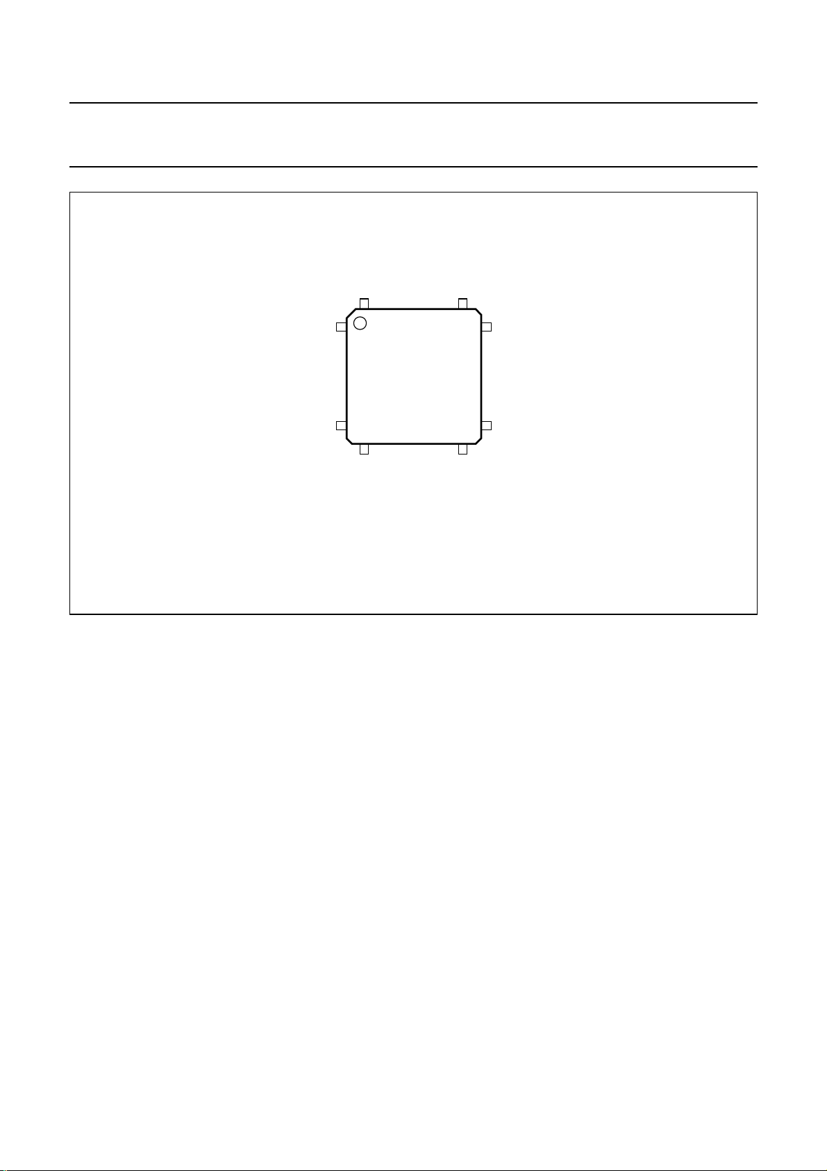
handbook, halfpage
40
160
1
SAA4978H
41
121
80
SAA4978H
120
81
MHB174
Fig.3 Pin configuration.
7 FUNCTIONAL DESCRIPTION
The SAA4978H consists of the following main functional
blocks:
• Analog preprocessing and analog-to-digital conversion
• Digital processing at 1fH level
• Digital processing at 2fH level
• Digital-to-analog conversion
• Line-locked clock generation
• Crystal oscillator
• Control interfacing I2C-bus and SNERT
• Register I/O
• Programmable Signal Positioner (PSP)
• 80C51 microcontroller core
• Board level testability provisions.
7.1 Analog input blocks
7.1.1 GAIN ELEMENTS FOR AUTOMATIC GAIN CONTROL
(9 dB RANGE)
A variable amplifier is used to map the possible YUV input
range to the analog-to-digital converter range e.g. as
defined for SCART signals.
According to this specification, a lift of 6 dB up to a drop of
3 dB may be necessary with respect to the nominal values.
The gain setting within the required minimum 9 dB range
is performed digitally via the internal microcontroller.
For this purpose a gain setting digital-to-analog converter
is incorporated. The smallest step in the gain setting
should be hardly visible on the picture, this can be met with
smaller steps of 0.4%/step.
Luminance and chrominance gain settings can be
separately controlled. The reason for this split is that
U and V may have already been gain adjusted by an
Automatic Chrominance Control (ACC), whereas
luminance is to be adjusted by the SAA4978H AGC.
However, for RGB originated sources, Y, U and V should
be adjusted with the same AGC gain.
7.1.2 C
LAMP CIRCUIT, CLAMPING Y TO DIGITAL LEVEL 32
AND UV TO 0(TWOS COMPLEMENT)
A clamp circuit is applied to each input channel, to map the
colourless black level in each video line (on the sync back
porch) to level 32 at 9 bits for Y and to the centre level of
the converters for U and V. During the clamp period, an
internally generated clamp pulse is used to switch-on the
clamp action.
1999 May 03 10
Page 11

Philips Semiconductors Product specification
Picture Improved Combined Network
(PICNIC)
A voltage controlled current source construction, which
references to voltage reference points in the ladders of the
analog-to-digital converters, provides a current on the
input of the YUV signals in order to bring the signals to the
correct DC value. This current is proportional to the DC
error, but is limited to±150 µA. It is essential that the clamp
current becomes zero with a zero error and that the
asymmetry between positive and negative clamp currents
is limited to within 10%. When the clamping action is off,
the residual clamp current should be very low, so that the
clamp level will not drift away within a video line.
The clamp level in the Y channel has a minimum value of
600 mV to ensure undisturbed clamping for maximum
Y input signals with top sync levels up to 600 mV. In order
to improve common mode rejection it is recommended to
connect the same source impedance as used in the YIN
input at the DIFFIN input to ground.
7.1.3 A
A 3rd-order linear phase filter is applied to each of the
Y, U and V channels. It provides a notch on f
at Y, U and V) to strongly prevent aliasing to low
frequencies, which would be the most disturbing.
The bandwidth of the filters is designed for −3 dB at
5.6 MHz. The filters can be bypassed if external filtering
with other characteristics is desired. In the bypass mode
the gain accuracy of the front-end part is 4% instead of 8%
for the filter-on mode.
7.1.4 9-
NALOG ANTI-ALIASING PREFILTER
BIT ANALOG-TO-DIGITAL CONVERSION
(16 MHz
clk
SAA4978H
7.2.2 Y
The Y samples can be shifted onto 4 positions with
respect to the UV samples. This shift is meant to account
for a possible difference in delay prior to the SAA4978H,
e.g. from a prefilter in front of an analog-to-digital
converter. The zero delay setting is suitable for the
nominal case of aligned input data according to the
interface format standard. One setting provides one
sampleless delay in Y, the other two settings provide more
delay in the Y path.
7.2.3 T
A circuit is added in the luminance channel to suppress the
typical multi-step trip level noise. This majority follower
filter compares the neighbouring pixels to a +1 or −1 LSB
difference. If the majority of these differences is +1 then 1
is added to the actual pixel. If the majority of these
differences is −1 then 1 is subtracted from the actual pixel.
The number of pixels included in the filter is selectable;
1 (bypass), 3, 5, 7 or 9.
7.2.4 N
The non-linear phase filter adjusts for possible group delay
differences in the luminance channel. The filter coefficients
are [−L × (1 − u); 1 + L; −L × u]; where L determines the
strength of the filter and u determines the asymmetry.
The effect of the asymmetry is that for higher frequencies
the delay is decreased for u ≤ 0.5. Settings are provided
for L = 0,1⁄16,2⁄16and3⁄16 and u = 0,1⁄4and1⁄2.
DELAY
RANSIENT NOISE SUPPRESSION
ON-LINEAR PHASE FILTER AFTER ADC
Three identical multi-step type analog-to-digital converters
are used to convert the Y, U and V inputs with a 16 MHz
data rate. The ADCs have a 2-bit overflow detection, and
an underflow detection for U and V, to be used for AGC
control. The 2 bits are coded for one in-range level and
three overflow levels; 1 dB, 1 to 2 dB and 2 to 3 dB.
7.2 Digital processing blocks
7.2.1 O
VERFLOW DETECTION
A histogram of the three overflow levels is made every field
and can be read in a 2-byte accuracy. An input selector
defines which ADC is monitored.
In the event of U or V selection the underflow information
is also added to the first histogram level, in this way the
data can be handled as out-of-range information.
The histogram content provides information for the AGC to
make an accurate estimate of the decrease in gain, in the
event of overflow for luminance or out-of-range detection
for U and V.
1999 May 03 11
7.2.5 4 MH
Z NOTCH
The 4 MHz notch provides a zero on1⁄4 of the sample
frequency. With fs= 16 MHz the notch is thus at 4 MHz.
The 3 dB notch width is 2 MHz. The filter coefficients are
1
⁄8× [−1; 0; 5; 0; 5; 0; −1]. This filter gives a relative gain of
0.75 dB at 1.7 and 6.3 MHz.
The notch can be bypassed without changing the group
delay.
7.2.6 D
IGITAL CLAMP CORRECTION FOR UV
During 32 samples within the active clamping the clamp
error is measured and accumulated to determine a
low-pass filtered value of the clamp error. A vertical
recursive filter is then used to further reduce this error
value. This value can be read by the microcontroller or be
used directly to correct the clamp error. It is also possible
for the microcontroller to give a fixed correction value.
Page 12

Philips Semiconductors Product specification
Picture Improved Combined Network
(PICNIC)
7.2.7 4:4:4DOWNSAMPLED TO 4:2:2OR 4:1:1
4:4:4 data is downsampled to 4 : 2 : 2, by first filtering
with a [1; 0; −7; 0; 38; 64; 38; 0; −7; 0; 1] filter, before being
subsampled by a factor of 2. The U and V samples from
the 4 :2:2 data are filtered again by a [−1; 0; 9; 16; 9; 0;
−1] filter, before being subsampled a second time by a
factor of 2. Bypassing this function keeps the data in the
4:2:2 format.
7.2.8 B
The chosen 4:1:1 or 4:2:2 formatted output data is
presented to bus A (YUV_A bus), consistent with the WEA
data enable signal. After the rising edge of WEA the first,
respectively second, data word contains the first phase of
the 4 :1:1 or 4:2:2 format, depending on the qualifier
respectively prequalifier mode of WEA. If the data has to
be formatted to 8 bits, a choice can be made between
rounding and dithered rounding. Dithered rounding may be
applied in the sense that every odd output sample has had
an addition of 0.25 LSB (relative to 8 bits) before
truncation and every even output sample has had an
addition of 0.75 LSB before truncation. In this way, on
average, correct rounding is realized (no DC shift).
Especially for low frequency signals, the resolution is
increased by a factor of 2 by the high frequency
modulation. The phase of dithering can be switched 180°
from line-to-line, field-to-field or frame-to-frame, in order to
decrease the visibility of the dithering pattern.
The not connected output pins of bus A, including WEA
(depending on the application), can be set to 3-state to
allow short-circuiting of these pins at board production.
Short-circuiting at not connected outputs can not be tested
by Boundary Scan Test (BST). For outputs in 3-state mode
it is not allowed to apply voltages higher than
V
DDO
7.2.9 B
Bus B can accommodate the following formats; 4 :1:1
serial, 4:2:2 parallel, 4:2:2 double clock UYVY, all
synchronous and asynchronous. All external formats are
selectable with prequalifier or qualifier WEB. All of the
various input formats are converted to the internal 9 bits
4:2:2. For the 8-bit inputs, the LSB of the input bus
should be connected externally to a fixed logic level. In the
event of a 4:1:1 input, the U and V channels are
reformatted and upsampled by generating the extra
samples with a1⁄16× [−1; 9; 9; −1] filter. The other U and V
samples remain equal to the original 4 :1:1 sample
values.
US A FORMAT: INTERFACE FORMATTING,TIMED
WITH ENABLING SIGNAL
+ 0.3 V.
US B FORMAT (see Table 1 and Fig.9)
(see Table 1 and Fig.9)
SAA4978H
It is possible, in bus B reformatter, to invert the UV data so
that the SAA4978H can handle any polarity convention of
the UV data.
In the event of an asynchronous input the clock has to be
provided externally to pin CLKAS.
When applying an external PALplus decoder with 30 ms
processing delay, the vertical field start can be set via
software in a PSP register. For
format input, inversion of the MSB of the (synchronized)
bus B UV input can be selected. Synchronization signals
included in this format will be ignored.
7.2.10 T
The Time Base Correction (TBC) and Sample Rate
Conversion (SRC) block provides a dynamically controlled
delay with an accuracy of up to1⁄64 of a pixel and a range
of −0.5 to +0.5 lines (plus processing delay).
The time base correction block has an input for skew data.
This skew data can be the phase error measured by a
HPLL, which is located in the PLL block of the SAA4978H.
The skew is used as a shift of the complete active video
part of a line. Added with a static (user controlled) shift, up
to1⁄2video line (32 µs) can be shifted in both directions,
related to a nominal1⁄2line delay.
For sample rate conversion, the delay is also varied along
the line with the subpixel accuracy. With a zero-order
variation of the delay, a linear compress or expand
function can be obtained. The range for the compression
factor is 0 to 2, meaning infinite zoom up to a compression
with a factor of 2. With a 2nd-order variation of the delay
added to the control, the compression factor can be
modulated with a parabolic shape, thus giving a panoramic
view option to display e.g. 4 : 3 video on a 16 : 9 screen or
vice versa.
The static shift may also be used to make the delay of the
SAA4978H plus periphery equal to an integer number of
lines. This is useful for 1fH applications, in which the
horizontal sync signal is not delayed with the video data.
This will then make the function of time base correction
obsolete for 1fH applications.
Another main task for the sample rate converter is to
resynchronize external data at a non-system clock sample
rate, for instance, MPEG decoder signals at 13.5 MHz.
A requirement for these signals is that they are line and
frame locked to the SAA4978H.
IME BASE CORRECTION AND SAMPLE RATE
CONVERSION
“CCIR 656”
standard data
1999 May 03 12
Page 13

Philips Semiconductors Product specification
Picture Improved Combined Network
(PICNIC)
7.2.11 NOISE REDUCTION
The noise reduction part consists of clamp noise reduction
and spatial noise reduction for low frequency noise. Within
this ensemble a two dimensional band split is used,
enabling also the functions of 2D low passing, adding the
multi Picture-In-Picture (multi PIP) function and 2D
peaking.
The clamp noise reduction is realized with an adaptive
temporal recursive filter. This filter will correct the DC level
of each line when it is varying from field-to-field in the
segments with the least likely movement. This clamp noise
filtering is intended to correct for clamp errors in a
complete chain, which cannot be removed with traditional
clamping on the back porch of the video. Clamp noise is
only reduced for luminance.
The spatial noise reduction is targeted for reduction of the
mid frequency noise spectrum, where adaptive filtering
combines pixels around the centre pixel and pixels from
the lines above in a recursive way. This spatial noise
reduction is only realized for luminance.
The 2D low-pass filter is a [1; 2; 1] filter in both the
horizontal and vertical direction. 2D high-pass is realized
by taking the centre tap and subtracting the 2D low-pass
output from it. Also added in the 2D high-pass is the
vertical low-passed data, which is subtracted from the
centre tap and multiplied by a user selectable gain
(0 to7⁄8). The 2D high-pass data is multiplied by a user
selectable gain of 0 and2⁄4to8⁄4 and cored before adding
it to the 2D low-pass branch for the 2D peaking function.
The HF signal bypasses both the LF temporal and the
spatial noise reduction, therefore sharpness in the high
frequencies is not reduced by the noise reduction parts.
The factor 0 on the HF signal yields a pure 2D low-passed
signal at the output. Multi PIP with pure subsampling of this
signal yields a much better result than without the low-pass
operation.
7.2.12 H
Histogram modification consists of acquiring the histogram
of the luminance levels and correcting the luminance
transfer curve in order to provide more perceptual contrast
in the picture.
ISTOGRAM
SAA4978H
The histogram acquisition uses 32 baskets on the grey
scale from (ultra) black to (ultra) white. Pixels that are
found around the centre of a basket increase a counter for
that basket with the value 8, pixels that come around the
edge between two baskets increase the counters in both
baskets, such as 3 in the left one and 5 in the right one.
By this method, the quantization distortion is overcome
from having a discrete set of baskets.
Between acquisition of the histogram and correction of the
transfer curves, the microcontroller included in the
SAA4978H processes the counter values from the
32 baskets. The outcome of the microcontrollers algorithm
defines a differential transfer curve for the luminance. This
means that only differences from a 1 : 1 transfer curve are
coded. This is done in 32 LUT points, with a linear
interpolation for all input values in between the LUT points.
When changes are made to the luminance level of pixels,
the saturation has to be restored by using the same
relative gain for the U and V channels.
The histogram data also provides the information of the
minimum and maximum levels of Y, U and V, by which the
microcontroller can affect an AGC gain before the video
analog-to-digital conversion.
Another main part of the histogram is the display-bars
block. This block can insert up to 32 horizontal bars in the
YUV data path. Size, spacing, luminance, colour and
length are fully programmable. This can be used to
construct a visual display of the histogram or transfer
curve.
7.2.13 S
Subtitle detection searches in a large area of the video
field for patterns that are characteristic for subtitles.
The expectation is to encounter in a video line a
considerable number of crossings through both a dark
grey and a light grey threshold and in its vicinity also
crossings in the other direction. This part is realized with
valid crossing (event) counting on each line in the target
area. This event value is stored for 128 lines in the subtitle
RAM, which is located at the top of the auxiliary RAM.
The subtitle logic has higher priority to access the subtitle
RAM than the microcontroller.
UBTITLE DETECTION
For economy, a subsampling is realized on the video with
a factor of 4 before the histogram is produced. From
line-to-line, a two pixel offset is used on the subsample
pattern.
1999 May 03 13
The internal microcontroller can filter out this data. In a
number of adjacent lines, there must be a similar high
count value for the number of events. If this condition holds
then the detection of subtitles on that vertical position is
more definite.
Page 14

Philips Semiconductors Product specification
Picture Improved Combined Network
(PICNIC)
This information can be used in combination with other
information on how to display the video source on the
screen. Such decisions are made entirely by the internal
microcontroller.
7.2.14 B
Black bar detection searches in the upper and in the lower
part of the screen to respectively the last black line and the
first black line. To avoid disturbances of Logos in the video,
measurements can be performed in only the horizontal
centre part of the lines.
7.2.15 B
The U and V samples from the 4 :2:2 data are filtered
again by a [−1; 0; 9; 16; 9; 0; −1] filter, before being
subsampled by a factor of 2. Bypassing this function keeps
the data in the 4 : 2 : 2 format.
Should it be required to format the data to 8 bits, a choice
can be made between rounding and dithered rounding.
Dithered rounding may be applied in the sense that every
odd output sample has had an addition of 0.25 LSB
(relative to 8 bits) before truncation and every even output
sample has had an addition of 0.75 LSB before truncation.
In this way, normally, correct rounding is realized (no DC
shift). Especially for low frequency signals, the resolution
is increased by a factor of 2 by the high frequency
modulation. The phase of dithering is switched 180° from
line-to-line, field-to-field or frame-to-frame in order to
decrease the visibility of the dithering pattern.
This block also performs the subsampling for multi PIP,
with subsampling factors of 1, 2, 3 and 4.
Another output format at bus C is Differential Pulse Code
Modulation (DPCM) 4 : 2 : 2. This data compression
method is applied on the U and V channels, and gives a
50% data reduction. In this way it is possible to convert a
4:2:2 picture to 2fH using a single 12-bit wide field
memory. This format is especially useful for graphics
conversion with high amplitude and high saturation input
signals. The not connected output pins of bus C including
WEC and IEC (depending on the application) can be set to
3-state to allow short-circuiting of these pins at board
production. Short-circuiting at not connected outputs can
not be tested by BST. For outputs in 3-state mode it is not
allowed to apply voltages higher than V
LACK BAR DETECTION
US C FORMAT (see Table 1)
DDO
+ 0.3 V.
SAA4978H
7.2.16 B
Bus D can handle 4 :1:1 external 8 or 9 bits, 4 : 2 : 2
external 8 or 9 bits, 4 : 2 : 2 internal 9 bits and DPCM
4:2:2.
Bus D is selectable in 1fH and 2fH mode. In 1fH mode the
internal input can also be used.
For dithered 8-bit luminance signals an undither block is
provided that restores the 9th bit for low frequency and low
noise. This is needed before the peaking circuit to prevent
amplification of the1⁄2fs dither modulation.
In the event of 8-bit inputs, the LSB of the input bus should
be externally connected to a fixed logic level.
In the event of a 4:1:1 input, the U and V channels are
reformatted and upsampled by generating the extra
samples with a1⁄16× [−1; 9; 9; −1] filter. The other U and V
samples remain equal to the original 4 :1:1 sample
values.
7.2.17 P
Peaking in the SAA4978H can be used in two ways:
1. The first way is to give the luminance a linear boost of
2. The second way is to use the peaking dynamically, in
Basically, the three peaking filters (1 high-pass and
2 band-pass) filter the incoming luminance signal.
The high-pass filter is made with [−1; 2; −1] coefficients,
giving a maximum throughput at1⁄2fs (equals 8 MHz).
The first band-pass filter has [−1; 0; 2; 0; −1] coefficients,
giving a maximum throughput at1⁄4fs (equals 4 MHz).
The second band-pass filter has a cascade of
[−1; 0; 0; 2; 0; 0; −1] and [1; 2; 1] coefficients, giving a
maximum throughput at 2.38 MHz.
With a separate gain control on each of the peaking filters
[possible gain settings of (0,1⁄16,2⁄16,3⁄16,4⁄16,5⁄16,6⁄
and8⁄16)], a desired frequency characteristic can be
obtained with steps of maximum 2 dB gain difference at
the centre frequencies.
US D REFORMATTER: THE VARIOUS INPUT
FORMATS ARE ALL CONVERTED TO THE INTERNAL
9 BITS 4:2:2(seeTable 1)
EAKING
the higher frequency ranges, which makes no
distinction between small and large details or edges.
order to boost smaller details and provide less gain on
large details and edges. The effect is detail
enhancement without the creation of unnaturally large
overshoots and undershoots on large details and
edges.
16
1999 May 03 14
Page 15

Philips Semiconductors Product specification
Picture Improved Combined Network
(PICNIC)
The sum of the filter outputs is fed through a coring circuit
with a user definable transfer curve between
−7 and +7 LSB at a 12-bit level. The definition of the coring
LUT is realized with two control registers. Herein, for each
of the points in the transfer curve, the user can define an
output between 0 and the input value. For the LUT
points +7 (and −7), a choice can be made from
(−4) +4 to (−7) +7. By setting control bit CORING to LOW,
the coring transfer curve is switched to a coarse coring
which is only dependent on the threshold (see Fig.13).
The so formed peaking signal can be added to the original
luminance signal, the sum of which then becomes the 9-bit
output signal (black-to-white), with an additional DA shift
fitting within 10 bits.
For dynamic use of the peaking circuit, an additional gain
is provided on the peaking signal. This gain is made
dependent on the energy in the peaking signal.
To overcome an unwanted coring on structured small
signals, the output of the low-pass filter is also used to
monitor if the high frequency contents are large enough to
refrain from coring. Therefore the coring is set off if the HF
energy level rises above a user definable threshold.
SAA4978H
7.2.19 DCTI
The Digital Colour Transient Improvement (DCTI) is
intended for U and V signals originating from a 4:1:1
source. Horizontal transients are detected and enhanced
without overshoots by differentiating, making absolute and
again differentiating the U and V signals separately. This
signal is used as a pointer to make a time modulation.
This results in a 4:4:4 UandV bandwidth. To prevent
third harmonic distortion, typical for this processing, a so
called ‘over the hill protection’ prevents peak signals from
becoming distorted. It is possible to control gain, width,
connect U and V and over the hill range via the
microcontroller.
At the output of the DCTI a post-filter is situated to make a
correction for the simple upsampling in DCTI which is a
linear interpolation [1; 2; 1]. The post-filter coefficients are
[−1; 2; 6; 2; −1], convolution of both filters gives
[−1; 0; 9; 16; 9; 0; −1]. This post-filter should only be used
when the DCTI is off, and the source material is 4 : 2 : 2
bandwidth.
7.2.20 B
ORDER BLANK
Spectral measurements are performed with the
spectr_meas subpart, by calculating the sum of the
absolute values from a chosen one of the three (high-pass
and band-pass) filter outputs over a vertical window in a
video field. With this window it is possible to disable
subtitles. The maximum value of the chosen filter output
within a windowed video field is also monitored. For the
generally lower HF contents of the video signal, a
weighting by a factor 4 can be switched in, while
measuring on the High-Pass Filter (HPF).
7.2.18 N
This non-linear phase filter adjusts for possible group
delay differences in the Y, U and V output channels, and
for sinus x/x bandwidth loss of the ADCs. The filter
coefficients are [−L × (1 − u); 1 + L; −L × u]; where
L determines the strength of the filter and u determines the
asymmetry. The effect of the asymmetry is that for higher
frequencies the delay is decreased for u ≤ 0.5. Settings
are provided for L = 0,1⁄8,2⁄8,3⁄8and u = 0,1⁄4,1⁄2.
ON-LINEAR PHASE FILTER BEFORE DAC
The border and blanking processing is operating at a
4:4:4 level, just before the analog-to-digital conversion.
Here it is possible to generate a blanking window and
within this window a border window. The blanking window
is used to blank the non-visible part of the output to the
clamp level. The border window is the visible part of the
video that contains no video, such as the sides in
compression mode, this part can be programmed to
display any luminance or colour level in an 8-bit accuracy;
pixel repetition is also possible here. In case of multi PIP
this block can generate separation borders in the
horizontal and vertical direction.
1999 May 03 15
Page 16

Philips Semiconductors Product specification
Picture Improved Combined Network
(PICNIC)
7.3 Analog output blocks
7.3.1 T
Three identical DACs are used to convert Y, U and V with
a 32 or 16 MHz data rate.
7.3.2 A
A 3rd-order linear phase filter is applied to each of the Y,
U and V channels. It provides a notch on f
U and V) to strongly prevent aliasing to low frequencies,
which would be most disturbing. The filters can be
bypassed if external filtering with other characteristics is
desired. Bandwidth and gain accuracy are given in
Chapter 11.
7.3.3 PLL
The PLL consists of a ring oscillator, Discrete Time
Oscillator (DTO) and digital control loop. The PLL
characteristic is controlled by means of the
microcontroller.
7.3.4 SNERT
A SNERT interface is built-in to transform the parallel data
from the microcontroller into 1 or 2 Mbaud switchable
SNERT data. This interface is also capable of reading data
from the SNERT bus should it be required to access read
registers.
The read or write operation must be set by the
microcontroller. When writing to the bus, 2 bytes are
loaded by the microcontroller; one for the address, the
other for the data. When reading from the bus, 1 byte is
loaded by the microcontroller for the address, the received
byte is the data from the addressed SNERT location.
The SNERT interface replaces the standard UART
interface. In contrast to the 80C51 UART interface there
are additional control registers, other I/O pads and no byte
separation time between address and data. After
power-on reset the 1 Mbaud mode is active. Switching
baud rate during transmission should be avoided.
7.3.5 PSP
For dynamically changing data such as timing signals, the
programmable signal positioner generates them on the
basis of parameters sent by the microcontroller. For the
reset function of the microcontroller, a watchdog timer is
also built-in that creates a reset pulse unless it is triggered
by a change in the Bone signal within a preset time
(1.05 s).
RIPLE 10-BIT DIGITAL-TO-ANALOG CONVERSION
NALOG ANTI-ALIASING POST-FILTER
(32 MHz at Y,
clk
SAA4978H
7.3.6 M
The SAA4978H contains an embedded 80C51
microcontroller core including a 1 kbyte RAM and a
32 kbyte ROM. It also includes an I2C-bus user control
interface. For development reasons an external ROM can
be accessed with 64 kbyte maximum size. An external
emulator can be connected.
The main difference to most existing 80C51 derivatives is:
• 768 byte auxiliary RAM from which 128 bytes can be
accessed as subtitle RAM
• Interrupt vector address for the I2C-bus is 33H
• On-chip ROM code protection
• SNERT at 1 or 2 Mbaud with additional Sample
Frequency Registers (SFRs) instead of UART
• Host interface containing all control registers access
e.g. via MOVX instruction.
7.3.7 B
Boundary scan test is implemented, according to
“IEEE standard 1149.1”
digital pins and will cover all connections from the
SAA4978H to other ICs that are also equipped with BST.
The connectivity of the analog YUV input/output pins can
also be tested with the use of BST.
The digital outputs UVAL, UVA0, UVA1, UVA2, UVA3,
YAL, UVCL, UVC0, UVC1, UVC2, UVC3, YCL, WEA,
WEC and IEC can be set in 3-state mode if not connected
in the application. This means that these outputs with
index 0 to 3 are set in 3-state if 4 :1:1 is chosen, and the
outputs with index L are set in 3-state if 8 bits output is
chosen.
7.3.8 P
All digital blocks except PLL are reset by a HIGH level at
the reset pin. Only the watchdog counter is reset by the
falling edge of the reset pulse. The PLL needs no reset.
The frequency guard generates a single reset pulse with a
duration of 0.875 ms when the actual frequency enters the
desired range of 14 to 18 MHz. If the frequency leaves this
range then no reset pulse is generated.
ICROCONTROLLER
OARD LEVEL TESTABILITY
. The boundary scan affects all
OWER-ON RESET
1999 May 03 16
Page 17

This text is here in white to force landscape pages to be rotated correctly when browsing through the pdf in the Acrobat reader.This text is here in
_white to force landscape pages to be rotated correctly when browsing through the pdf in the Acrobat reader.This text is here inThis text is here in
white to force landscape pages to be rotated correctly when browsing through the pdf in the Acrobat reader. white to force landscape pages to be ...
1999 May 03 17
8 CONTROL REGISTER DESCRIPTION
NAME
Clamp registers (clamp position in steps of one pixel, only first quarter of line available)
CLAMP_START 300 write XXXXXXXXclamp start position
CLAMP_STOP 301 write XXXXXXXXclamp stop position
AGC
AGC_GAIN_Y 302 write XXXXXXXXXset Y gain (−3to+6dB)
AGC_GAIN_U 303 write XXXXXXXXXset U gain (−3to+6dB)
AGC_GAIN_V 304 write XXXXXXXXXset V gain (−3to+6dB)
Overflow detection control
YUV_SELECT 305 write X X select ADC (Y, U, V, V)
OVERFLOW_11_HIGH 300 read E XXXXXXXXread HIGH byte level 11
OVERFLOW_11_LOW 301 read E XXXXXXXXread LOW byte level 11
OVERFLOW_10_HIGH 302 read E XXXXXXXXread HIGH byte level 10
OVERFLOW_10_LOW 303 read E XXXXXXXXread LOW byte level 10
OVERFLOW_01_HIGH 304 read E XXXXXXXXread HIGH byte level 01;
OVERFLOW_01_LOW 305 read E XXXXXXXXread LOW byte level 01;
ADDRESS
HEX
READ/
WRITE
DOUBLE
BUFFERED
876543210 DESCRIPTION
(1)
underflow/overflow
underflow/overflow
Philips Semiconductors Product specification
Picture Improved Combined Network
(PICNIC)
Digital front-end
DFRONTEND_CONTROLS1 306 write XXXXXXXX
U_CLAMP_COR_FVAL XXXUclamp correction value
(twos complement) used in external
correction mode
V_CLAMP_COR_FVAL X X X V clamp correction value
(twos complement) used in external
correction mode
UV_COR_MODE X X UV clamp correction mode (internal,
external, keep, keep)
DFRONTEND_CONTROLS2 307 write XXXXXXX
UV_TAU X X select UV clamp time constant
(4, 9, 19 and 39 lines)
Y_DELAY X X select Y delay (−1, 0, 1, 2)
SAA4978H
Page 18

This text is here in white to force landscape pages to be rotated correctly when browsing through the pdf in the Acrobat reader.This text is here in
_white to force landscape pages to be rotated correctly when browsing through the pdf in the Acrobat reader.This text is here inThis text is here in
white to force landscape pages to be rotated correctly when browsing through the pdf in the Acrobat reader. white to force landscape pages to be ...
1999 May 03 18
NAME
MFF_WIDTH X X X select MFF width
DFRONTEND_CONTROLS3 308 write XXXXX
NLP_L_AD X X input λ settings (0,
NLP_U_AD X X input µ settings (0,
NOTCH X select notch (off, on)
ACT_VIDEO_WINDOW_H_START 309 write XXXXXXXX
ACT_VIDEO_WINDOW_H_LENGTH 30A write XXXXXXXX
ACT_VIDEO_WINDOW_V_START 30B write XXXXXXXXX
ACT_VIDEO_WINDOW_V_LENGTH 30C write S XXXXXXXXXnot double buffered for PSP (WEA)
CLAMP_U_ERROR 306 read 0 XXXXXXXclamp offset in U (twos complement;
CLAMP_V_ERROR 307 read 0 XXXXXXXclamp offset in V (twos complement;
ADDRESS
HEX
READ/
WRITE
DOUBLE
BUFFERED
876543210 DESCRIPTION
(1)
(0, 3, 5, 7, 9, 9, 9 and 9 samples)
gain 16) used in internal correction
mode
gain 16) used in internal correction
mode
1
⁄16,2⁄16,3⁄16)
1
⁄4,1⁄2,1⁄2)
Philips Semiconductors Product specification
Picture Improved Combined Network
(PICNIC)
Bus A output control
BUS_A_CONTROL1 30D write XXXXXXXX
Y_BUS_A_8BIT_ROUND X X Y bus A (9-bit rounded, 9-bit rounded,
8-bit dithered, 8-bit truncated)
Y_BUS_A_DITHER X X X dithering mode on Y bus A (F1L1,
F1L2, F1L1,F1L2, F2L1, F2L2, F4L1,
F4L2)
SEL_422_OUT X select 4 :2:2 output format (4:1:1,
4:2:2)
UV_CORING X X select UV coring mode
(off, 0.5, 1.0, 1.5 LSB)
BUS_A_CONTROL2 30E write XXXXXXX
UV_BUS_A_8BIT_ROUND X X UV bus A (9-bit rounded,
9-bit rounded, 8-bit dithered,
8-bit rounded)
UV_BUS_A_DITHER X X X dithering mode on UV bus A (F1L1,
F1L2, F1L1, F1L2, F2L1, F2L2, F4L1,
F4L2)
SAA4978H
Page 19

This text is here in white to force landscape pages to be rotated correctly when browsing through the pdf in the Acrobat reader.This text is here in
_white to force landscape pages to be rotated correctly when browsing through the pdf in the Acrobat reader.This text is here inThis text is here in
white to force landscape pages to be rotated correctly when browsing through the pdf in the Acrobat reader. white to force landscape pages to be ...
1999 May 03 19
NAME
FORCE_BUS_A_TRI X force bus A output to 3-state including
WE_A_QUALIFIER X WEA definition (prequalifier, qualifier)
Bus B input control
BUS_B_CONTROL 30F write XXXXXXX
SEL_INPUT_FORMAT X X select input format (4 : 2 : 2 external,
SEL_DOUBLE_CLOCK X select double input data rate (single,
SEL_ASYNCHRONOUS X select asynchronous input clock
UV_INV X invert U and V data (not inverted,
WE_B_QUALIFIER X WEB definition (prequalifier, qualifier)
INV656 X invert MSB of bus B input (related to
ADDRESS
HEX
READ/
WRITE
DOUBLE
BUFFERED
876543210 DESCRIPTION
(1)
WEA (off, on)
4:1:1external, 4:2:2 internal,
4:2:2 internal)
double clock)
(synchronous, asynchronous clock)
inverted)
656 based input)
Philips Semiconductors Product specification
Picture Improved Combined Network
(PICNIC)
TBC/SRC control
C0 310 write S XXXXXXXXXcontrol of compression/expansion at
line centre (twos complement:
−256 to +255)
C2 311 write S XXXXXXXXcontrol of compression/expansion at
line edges (twos complement:
−128 to +127)
H_SHIFT_HIGH 312 write S XXXXXXXXhorizontal shift (bits 15 to 8)
H_SHIFT_LOW 313 write S XXXXXXXXhorizontal shift (bits 7 to 0)
H_DATAPATH_DELAY 314 write S XXXXXXXXhorizontal data path delay (bits 7 to 0)
H_DATAPATH_DELAY_SKEW 315 write S XXXXXXX
H_DATAPATH_DELAY_MSB XXXXXhorizontal data path delay
(bits 12 to 8)
SKEW_MUL T X X skew multiply factor (off, 1, undefined,
−1)
SAA4978H
Page 20

This text is here in white to force landscape pages to be rotated correctly when browsing through the pdf in the Acrobat reader.This text is here in
_white to force landscape pages to be rotated correctly when browsing through the pdf in the Acrobat reader.This text is here inThis text is here in
white to force landscape pages to be rotated correctly when browsing through the pdf in the Acrobat reader. white to force landscape pages to be ...
1999 May 03 20
NAME
Noise estimator
LIMERIC_THR_UP 316 write XXXXXXXXthreshold to define the weight factor of
LIMERIC_WANTED_VALUE 317 write S XXXXXXXXsensitivity of noise estimator
LIMERIC_TASTE_AND_COMP 318 write S XXXXXXXX
TASTE_VALUE XXXXtaste value
COMPENSATION_VALUE XXXX compensation value
LIMERIC_LB_DETAIL 319 write S XXXXXXXXbottom limit of detail counter
LIMERIC_UB_DETAIL 31A write S XXXXXXXXtop limit of detail counter
LIMERIC_YP_AND_OVLPL 31B write S XXXXXXXX
OVERLAP_VALUE XXXXoverlap level for noise estimator
PREFILTER_SCALING X X luminance prefilter scaling
SOB_NEGLECT X neglects the Sum Over a Block value
INPUT8BIT X number of bits at input of NE block
NEST 308 read E 0000XXXXnoise estimator value
NEST_FILT 309 read E XXXXXXXXfiltered noise estimator value
DETAIL_CNT_H 30A read E XXXXXXXXnumber of details detected in field
DETAIL_CNT_L 30B read E XXXXXXXXnumber of details detected in field
ADDRESS
HEX
READ/
WRITE
DOUBLE
BUFFERED
876543210 DESCRIPTION
(1)
considered pixels
(twos complement)
(0 to 15)
1
(1,
⁄2,1⁄4,off)
of those blocks that contain values
towards black and white;
(use, neglect) = (measure except
around black and white level, measure
everywhere
(9, 8)
(HIGH byte)
(LOW byte)
Philips Semiconductors Product specification
Picture Improved Combined Network
(PICNIC)
SAA4978H
Page 21

This text is here in white to force landscape pages to be rotated correctly when browsing through the pdf in the Acrobat reader.This text is here in
_white to force landscape pages to be rotated correctly when browsing through the pdf in the Acrobat reader.This text is here inThis text is here in
white to force landscape pages to be rotated correctly when browsing through the pdf in the Acrobat reader. white to force landscape pages to be ...
1999 May 03 21
NAME
Clamp noise reduction (CLINIC) control
CLINIC_CONTROL 31C write S XXXXXX
K_SCALE X X X select K scale
K_ONE X select K is 1 versus adaptive
CLINIC_OFF X CLINIC function off (on, off)
DITHER X dither on (off, on)
CLINIC_MAX_DIFF 31D write S XXXXXXXXmaximum difference allowed between
CLINIC_THRESHOLD 31E write S XXXXXXXXthreshold to define motion in
CLINIC_DIF_AND_THR_LSB 31F write S XXXX
MAX_DIFF_LSB X X maximum difference allowed between
THRESHOLD_LSB X X threshold to define motion in
NBR_EVENTS 30C read E XXXXXXXXnumber of events per field with motion
TOT_COR_H 30D read E XXXXXXXXaccumulated absolute clamp
TOT_COR_M 30E read E XXXXXXXXaccumulated absolute clamp
TOT_COR_L 30F read E 00000X X X accumulated absolute clamp
ADDRESS
HEX
READ/
WRITE
DOUBLE
BUFFERED
876543210 DESCRIPTION
(1)
1
(4, 2, 1,
(adaptive, K = 1)
actual and stored segment value
(bits 9 to 2)
segments (bits 9 to 2)
actual and stored segment value
(bits 1 and 0)
segments (bits 1 and 0)
above threshold
correction in field (bits 18 to 11)
correction in field (bits 10 to 3)
correction in field (bits 2 to 0)
⁄2,1⁄4,1⁄8,1⁄16,1⁄32)
Philips Semiconductors Product specification
Picture Improved Combined Network
(PICNIC)
Line memory and noise reduction (LIMERIC) control
LIMERIC_CONTROL 320 write S XXXXXXXX
N_DIST X X select n_dist (2, 4, 8, 9)
PC_DIST X X select pc_dist (1, 2, 3, 4)
PE_DIST X X select pe_dist (5, 6, 7, 8)
SAA4978H
Page 22

This text is here in white to force landscape pages to be rotated correctly when browsing through the pdf in the Acrobat reader.This text is here in
_white to force landscape pages to be rotated correctly when browsing through the pdf in the Acrobat reader.This text is here inThis text is here in
white to force landscape pages to be rotated correctly when browsing through the pdf in the Acrobat reader. white to force landscape pages to be ...
1999 May 03 22
NAME
ADDRESS
HEX
READ/
WRITE
DOUBLE
BUFFERED
876543210 DESCRIPTION
(1)
WEA VE X weave on (off, on)
SEL_N_THR X select threshold from estimator versus
threshold from microcontroller
(estimator, microcontroller)
Band split peaking and coring
PEAKING_CONTROL1 321 write S XXXX XXX
2D_PEAK_COEF X X X 2D peaking coefficient
2
(0,
⁄4,3⁄4,4⁄4,5⁄4,6⁄4,7⁄4,8⁄4)
CORE_THR XXXX coring threshold (0, 1, 2, 3, 4, 5, 6, 7,
8, 9, 10, 11,12, 13, 14, 15 LSB)
V_GAINSTR 322 write S X X X vertical peaking
1
(0,
⁄8,2⁄8,3⁄8,4⁄8,5⁄8,6⁄8,7⁄8)
Noise reduction energy measurement
VHF_ENERGY_SUM_H 310 read E XXXXXXXXmean vertical energy measured in one
field (bits 15 to 8)
VHF_ENERGY_SUM_L 311 read E XXXXXXXXmean vertical energy measured in one
field (bits 7 to 0)
VHF_ENERGY_MAX 312 read E XXXXXXXXmaximum vertical peak energy
measured in one field
Philips Semiconductors Product specification
Picture Improved Combined Network
(PICNIC)
Black bar position and control
BBD_FIRST_VIDEOLINE1 313 read E XXXXXXXX1⁄2number of first line after black bar
having video
1
BBD_LAST_VIDEOLINE1 314 read E XXXXXXXX
⁄2number of last line before black bar
having video
BBD_FIRST_VIDEOLINE2 315 read E XXXXXXXX
1
⁄2(number + 1) of first line after black
bar having video
BBD_LAST_VIDEOLINE2 316 read E XXXXXXXX
1
⁄2(number + 1) of last line before
black bar having video
BBD_WINDOW_H_START 323 write S XXXXXXXX
BBD_WINDOW_H_STOP 324 write S XXXXXXXX
BBD_WINDOW_V_START 325 write S XXXXXXXXX
BBD_WINDOW_V_STOP 326 write S XXXXXXXXX
SAA4978H
Page 23

This text is here in white to force landscape pages to be rotated correctly when browsing through the pdf in the Acrobat reader.This text is here in
_white to force landscape pages to be rotated correctly when browsing through the pdf in the Acrobat reader.This text is here inThis text is here in
white to force landscape pages to be rotated correctly when browsing through the pdf in the Acrobat reader. white to force landscape pages to be ...
1999 May 03 23
NAME
BBD_LOGO_LENGTH 327 write S XXXXXXXXnumber of non-black samples
BBD_SLICE_LEVEL1 328 write S XXXXXXXX1⁄2threshold to detect black
BBD_SLICE_LEVEL2 329 write S XXXXXXXX
Histogram control
BLACK_OFFSET 32A write S XXXXXXXXdefinition of DC shift in Y
LUT_DATA 32B write XXXXXXXXtransfer of 32 bytes that define the
THRESHOLD_HIS 32C write S XXXXXXXXifYn−Y
SPLIT_POSITION 32D write S XXXXXXXXposition of split point in steps of
HISTOGRAM_CONTROL1 32E write XXXXXXXnot double buffered
HISTO_GAIN XXXXhistogram gain (0 to 15)
NOISE_RED X noise reduction on
FILTER_1_ON X 1:2:1 filter on (off, on)
FILTER_2_ON X 1 :0:2:0:1 filter on (off, on)
RESERVED WRITE ADDRESS 32F write
YUV_IN_CONTROL 330 write S X X X X X
ROUND X rounding versus truncating
RATIO_LIMIT X select UV ratio 128 versus 64
UV_POS X follow if dy > 0 versus follow dy
UV_GAIN X X UV gain (0,
HGM_WINDOW_H_START 331 write S XXXXXXXXstart of horizontal histogram window
ADDRESS
HEX
READ/
WRITE
DOUBLE
BUFFERED
876543210 DESCRIPTION
(1)
permitted in a black bar line
(detector 1)
1
⁄2threshold to detect black
(detector 2)
(twos complement)
Y transfer LUT from microcontroller to
histogram (twos complement). The
first write after a field reset resets the
write pointer; subsequent write
operations increment the write pointer.
> threshold then Yn is
n−1
added to the histogram
4 pixels (left side unprocessed)
(truncated, rounded)
(64, 128)
(follow dy, follow if dy > 0)
1
⁄2,1,2)
Philips Semiconductors Product specification
Picture Improved Combined Network
(PICNIC)
SAA4978H
Page 24

This text is here in white to force landscape pages to be rotated correctly when browsing through the pdf in the Acrobat reader.This text is here in
_white to force landscape pages to be rotated correctly when browsing through the pdf in the Acrobat reader.This text is here inThis text is here in
white to force landscape pages to be rotated correctly when browsing through the pdf in the Acrobat reader. white to force landscape pages to be ...
1999 May 03 24
NAME
HGM_WINDOW_H_STOP 332 write S XXXXXXXXstop of horizontal histogram window
HGM_WINDOW_V_START 333 write S XXXXXXXXXstart of vertical histogram window
HGM_WINDOW_V_STOP 334 write S XXXXXXXXXstop of vertical histogram window
Histogram outputs
HISTOGRAM_DATA 317 read XXXXXXXXHistogram read command. The first
Y_MIN 318 read E XXXXXXXXminimum Y value in previous field
Y_MAX 319 read E XXXXXXXXmaximum Y value in previous field
U_MIN 31A read E XXXXXXXXminimum U value in previous field
U_MAX 31B read E XXXXXXXXmaximum U value in previous field
V_MIN 31C read E XXXXXXXXminimum V value in previous field
V_MAX 31D read E XXXXXXXXmaximum V value in previous field
MAX_HISTO_VALUE 31E read E XXXXXXXXmaximum value in histogram of
SMART_BLACK 31F read E XXXXXXXXblack level indication (filtered Y_MIN)
ADDRESS
HEX
READ/
WRITE
DOUBLE
BUFFERED
876543210 DESCRIPTION
(1)
read after a field reset resets the read
pointer; subsequent read operations
increment the read pointer.
previous field
Philips Semiconductors Product specification
Picture Improved Combined Network
(PICNIC)
Subtitle control
THRESHOLD_HIGH 335 write XXXXXXXXmaximum level required for valid event
THRESHOLD_LOW 336 write XXXXXXXXminimum level required for valid event
HIGH_TIME 337 write XXXXXXXXminimum time above HIGH threshold
required for valid event
LOW_TIME 338 write XXXXXXXXminimum time below LOW threshold
required for valid event
SUBTITLE_CONTROLS 339 write X X X
RESET_EVENTS X reset events (cumulative, reset)
EVENT_MODE X select event versus between
thresholds mode (within thresholds,
events)
RESET_PEAK X select ‘every field’ versus ‘bleed’
(bleed, every field)
SUBT_WINDOW_H_START 33A write XXXXXXXX
SAA4978H
Page 25

This text is here in white to force landscape pages to be rotated correctly when browsing through the pdf in the Acrobat reader.This text is here in
_white to force landscape pages to be rotated correctly when browsing through the pdf in the Acrobat reader.This text is here inThis text is here in
white to force landscape pages to be rotated correctly when browsing through the pdf in the Acrobat reader. white to force landscape pages to be ...
1999 May 03 25
NAME
SUBT_WINDOW_H_STOP 33B write XXXXXXXX
SUBT_WINDOW_V_ST ART 33C write XXXXXXXXX
SUBT_WINDOW_V_STOP 33D write XXXXXXXXX
EVENTS 280 to 2FF read XXXXXXXXEvents read command. Number of
RESERVED READ ADDRESS 320 read
PEAK_Y 321 read E XXXXXXXX
Bars control
BAR_ARRAY 33E write XXXXXXXXBar array write command. The first
BAR_ARRAY_Y 33F write S XXXXXXXXdisplay bar luminance level
BAR_ARRAY_U 340 write S XXXXXXXXdisplay bar U level (twos complement)
BAR_ARRAY_V 341 write S XXXXXXXXdisplay bar V level (twos complement)
BAR_ARRAY_H_START 342 write S XXXXXXXXhorizontal start position of the display
BAR_ARRAY_V_START 343 write S XXXXXXXXvertical start position of the display
BAR_ARRAY_WIDTH 344 write S XXXXXXXXthe width of each bar in number of
BAR_ARRAY_SPACE 345 write S XXXXXXXXthe number of lines between two bars
BAR_ARRAY_CONTROL 346 write S X X X
BAR_ARRAY_ON X select bar array on (off, on)
ADDRESS
HEX
READ/
WRITE
DOUBLE
BUFFERED
876543210 DESCRIPTION
(1)
transitions in the 128 lines of the
subtitle window.
1
⁄2peak value of Y within the event
window
write after a field reset resets the write
pointer; subsequent write operations
increment the write pointer (see also
BAR_ARRAY_RESOLUTION).
bars (see also
BAR_ARRAY_RESOLUTION)
bars
lines (see also
BAR_ARRAY_RESOLUTION)
(see also
BAR_ARRAY_RESOLUTION)
Philips Semiconductors Product specification
Picture Improved Combined Network
(PICNIC)
SAA4978H
Page 26

This text is here in white to force landscape pages to be rotated correctly when browsing through the pdf in the Acrobat reader.This text is here in
_white to force landscape pages to be rotated correctly when browsing through the pdf in the Acrobat reader.This text is here inThis text is here in
white to force landscape pages to be rotated correctly when browsing through the pdf in the Acrobat reader. white to force landscape pages to be ...
1999 May 03 26
NAME
BAR_ARRA Y_RESOLUTION X select bar array resolution
BAR_ARRAY_TRANS X select mashing versus superimpose
Bus C output control
BUS_C_CONTROL1 347 write S XXXXXXXX
SEL422OUT X select 4 :2:2 output (4:1:1,
UV_BUS_C_8BIT_ROUND X X UV bus C (9-bit rounded,
MPIP X X multi-PIP mode (off, 2 × 2, 3 × 3,
UV_BUS_C_DITHER X X X dither line and field phase (f1l1, f1l2,
BUS_C_CONTROL2 348 write S XXXXXXX
DPCM X DPCM output (4 :1:1/4:2:2,
FORCE_BUS_C_TRI X force bus C to 3-state including WEC
Y_BUS_C_8BIT_ROUND X X Y bus C (9-bit rounded, 9-bit rounded,
Y_BUS_C_DITHER X X X dither line and field phase (f1l1, f1l2,
ADDRESS
HEX
READ/
WRITE
DOUBLE
BUFFERED
876543210 DESCRIPTION
(1)
(BAR_ARRAY_H_START × 4,
BAR_ARRAY_WIDTH × 2,
BAR_ARRAY_SPACE × 2,
BAR_ARRAY × 4,
BAR_ARRAY_H_START × 2,
BAR_ARRAY_WIDTH × 1,
BAR_ARRAY_SPACE × 1,
BAR_ARRAY × 2)
(superimpose, mashing)
4 : 2 : 2) overridden by DPCM
9-bit rounded, 8-bit dithered,
8-bit truncated)
4 × 4); see also memory write control
f1l1, f1l2, f2l1, f2l2, f4l1, f4l2)
DPCM) overrides SEL422OUT
and IEC (off, on)
8-bit dithered, 8-bit truncated)
f1l1, f1l2, f2l1, f2l2, f4l1, f4l2)
Philips Semiconductors Product specification
Picture Improved Combined Network
(PICNIC)
SAA4978H
Page 27

This text is here in white to force landscape pages to be rotated correctly when browsing through the pdf in the Acrobat reader.This text is here in
_white to force landscape pages to be rotated correctly when browsing through the pdf in the Acrobat reader.This text is here inThis text is here in
white to force landscape pages to be rotated correctly when browsing through the pdf in the Acrobat reader. white to force landscape pages to be ...
1999 May 03 27
NAME
Field memory control
WE_WINDOW_H_START 349 write XXXXXXXXstart of horizontal write enable window
WE_WINDOW_H_STOP 34A write XXXXXXXXstop of horizontal write enable window
ACQ_EN_WINDOW_V_START 34B write XXXXXXXXXstart of vertical write and input enable
ACQ_EN_WINDOW_V_STOP 34C write XXXXXXXXXstop of vertical write and input enable
IE_WINDOW_H_START 34D write XXXXXXXXstart of horizontal input enable window
IE_WINDOW_H_STOP 34E write XXXXXXXXstop of horizontal input enable window
WE_IE_SHIFT 34F write XXXX
WE_C_SHIFT X X fine shift of WEC (0, 1, 2, 3 pixels)
IE_C_SHIFT X X fine shift of IEC (0, 1, 2, 3 pixels)
CHOP_CYCLE 350 write X X chop cycle of WEC and IEC
RE_WINDOW_H_START 351 write XXXXXXXXdefine start of horizontal read enable
RE_WINDOW_H_STOP 352 write XXXXXXXXdefine stop of horizontal read enable
RE_WINDOW_V_START 353 write XXXXXXXXXdefine start of vertical read enable
RE_WINDOW_V_STOP 354 write XXXXXXXXXdefine stop of vertical read enable
ADDRESS
HEX
READ/
WRITE
DOUBLE
BUFFERED
876543210 DESCRIPTION
(1)
window
window
1
(1,
⁄2,1⁄3,1⁄4)
window
window
window
window
Philips Semiconductors Product specification
Picture Improved Combined Network
(PICNIC)
Bus D input control
BUS_D_CONTROL 355 write S X X X
SEL_INPUT_FORMAT X X select input format (4 : 2 : 2 external,
4:1:1external, 4:2:2 internal,
DPCM external)
UNDITHER X select undither active (off, on)
BE_WINDOW_H_START 356 write XXXXXXXX
BE_WINDOW_H_STOP 357 write XXXXXXXX
BE_WINDOW_V_START 358 write XXXXXXXXX
BE_WINDOW_V_STOP 359 write XXXXXXXXX
SAA4978H
Page 28

This text is here in white to force landscape pages to be rotated correctly when browsing through the pdf in the Acrobat reader.This text is here in
_white to force landscape pages to be rotated correctly when browsing through the pdf in the Acrobat reader.This text is here inThis text is here in
white to force landscape pages to be rotated correctly when browsing through the pdf in the Acrobat reader. white to force landscape pages to be ...
1999 May 03 28
NAME
ADDRESS
HEX
READ/
WRITE
DOUBLE
BUFFERED
876543210 DESCRIPTION
(1)
CTI control
DBACKEND_CONTROLS1 35A write XXXXXX
CTI_SEPARATE X separate U and V processing (linked,
separate)
CTI_PROTECTION X select hill protection (off, on)
1
CTI_GAIN X X X CTI gain (0,
⁄8,2⁄8,3⁄8,4⁄8,5⁄8,6⁄8,7⁄8)
CTI_FILTER_ON X post-filter on (off, on)
DBACKEND_CONTROLS2 35B write XXXXXXXX
CTI_LIMIT X X limit CTI range (0, ±4, ±8, ±12)
CTI_SUPERHILL X select super hill protection (off, on)
CTI_DDX_SEL X select first differentiating filter
(−1 0 0 1, −1 −2 −1 1 2 1)
CTI_SUPERHILL XXXX hill detection threshold (0, 1, 2, 3, 4, 5,
6, 7, 8, 9, 10, 11,12, 13, 14, 15)
NLP_DA 35C write XXXX
NLP_L_DA X X output λ settings (0,
NLP_U_DA X X output µ settings (0,
1
⁄8,2⁄8,3⁄8)
1
⁄4,1⁄2,1⁄2)
Philips Semiconductors Product specification
Picture Improved Combined Network
(PICNIC)
Dynamic peaking and coring
PEAKING_CONTROL2 35D write S XXXXXXXX
ALPHA XXXαvalue
1
(0,
⁄16,2⁄16,3⁄16,4⁄16,5⁄16,6⁄16,8⁄16)
BETA XXX βvalue
1
(0,
⁄16,2⁄16,3⁄16,4⁄16,5⁄16,6⁄16,8⁄16)
DELTA XX δvalue (0,
1
⁄4,1⁄2,1)
LUTREGA 35E write S XXXXXXXXprogrammable coring replacement
values for luminance levels 1 to 4
LEVEL1 X level 1 (0, 1)
LEVEL2 X X level 2 (0, 1, 2, 3)
LEVEL3 X X level 3 (0, 1, 2, 3)
LEVEL4 X X X level 4 (0, 1, 2, 3, 4, 5, 6, 7)
LUTREGB 35F write S XXXXXXXXprogrammable coring replacement
values for luminance levels 5 to 7
SAA4978H
Page 29

This text is here in white to force landscape pages to be rotated correctly when browsing through the pdf in the Acrobat reader.This text is here in
_white to force landscape pages to be rotated correctly when browsing through the pdf in the Acrobat reader.This text is here inThis text is here in
white to force landscape pages to be rotated correctly when browsing through the pdf in the Acrobat reader. white to force landscape pages to be ...
1999 May 03 29
NAME
LEVEL5 X X X level 5 (0, 1, 2, 3, 4, 5, 6, 7)
LEVEL6 X X X level 6 (0, 1, 2, 3, 4, 5, 6, 7)
LEVEL7 X X level 7 (4, 5, 6, 7)
COR_THR 360 write S XXXXXXXXlocal energy above coring-threshold
PEAKING_CONTROL3 361 write S XXXXXXXX
TAU XXXτvalue
NEGGAIN X X negative gain value (0,
CORING X coring (coarse, fine) in accordance
ENERGY_SEL X X energy select (high × 4, mid, low, high)
ENERGY_SELECT_V_ST AR T 362 write XXXXXXXXXstart of vertical energy select window
ENERGY_SELECT_V_STOP 363 write XXXXXXXXXstop of vertical energy select window
RESERVED READ ADDRESS 322 read E XXXXXXXX
RESERVED READ ADDRESS 323 read E XXXXXXXX
ENERGY_MAX 324 read E XXXXXXXXmaximum peak energy measured in
ADDRESS
HEX
READ/
WRITE
DOUBLE
BUFFERED
876543210 DESCRIPTION
(1)
switches off coring
1
(0,
⁄16,2⁄16,3⁄16,4⁄16,5⁄16,6⁄16,8⁄16)
with LUTREGA and LUTREGB;
see Fig.13
one field
1
⁄4,1⁄2,1)
Philips Semiconductors Product specification
Picture Improved Combined Network
(PICNIC)
Blanking control (definition of blanking window)
BLANKING_WINDOW_H_START 364 write XXXXXXXX
BLANKING_WINDOW_H_STOP 365 write XXXXXXXX
BLANKING_WINDOW_V_START 366 write XXXXXXXXX
BLANKING_WINDOW_V_STOP 367 write XXXXXXXXX
Border control
BORDER_SIDE_H_START 368 write XXXXXXXXstart of right border
BORDER_SIDE_H_STOP 369 write XXXXXXXXend of left border
BORDER_SIDE_V_START 36A write XXXXXXXXXstart of lower border
BORDER_SIDE_V_STOP 36B write XXXXXXXXXstop of upper border
BORDER_BAR_H_START 36C write XXXXXXXXstart of first horizontal bar
BORDER_BAR_H_WIDTH 36D write XXXXXXXXwidth of horizontal bars
BORDER_BAR_V_START 36E write XXXXXXXXXstart of first vertical bar
SAA4978H
Page 30

This text is here in white to force landscape pages to be rotated correctly when browsing through the pdf in the Acrobat reader.This text is here in
_white to force landscape pages to be rotated correctly when browsing through the pdf in the Acrobat reader.This text is here inThis text is here in
white to force landscape pages to be rotated correctly when browsing through the pdf in the Acrobat reader. white to force landscape pages to be ...
1999 May 03 30
NAME
BORDER_BAR_V_WIDTH 36F write XXXXXXXXXwidth of vertical bars
BORDER_REPEAT_H 370 write XXXXXXXXhorizontal repeat value
BORDER_REPEAT_V 371 write XXXXXXXXXvertical repeat value
BORDER_Y 372 write XXXXXXXXYvalue of sides and bars
BORDER_U 373 write XXXXXXXXUvalue of sides and bars
BORDER_V 374 write XXXXXXXXVvalue of sides and bars
PLL
PLL_CK_AND_CD 375 write V XXXXXXXX
PLL_CK V XXXXXKfactor control (0 to 31)
PLL_CD V X X X damping control (0 to 7)
PLL_IDTO_PLUS_VARIOUS 376 write X X X X X X
PLL_IDTO(18-16) V X X X increment offset for DTO bits 18 to 16
PLL_OFF X PLL off; keep output frequency
PLL_OPEN V X PLL open loop mode (closed, open)
DO_SNAP X do snapshot
PLL_IDTO(15-8) 377 write V XXXXXXXXincrement offset for DTO bits 15 to 8
PLL_IDTO(7-0) 378 write V XXXXXXXXincrement offset for DTO bits 7 to 0;
PLL_SKEW_DELAY 379 write X X X skew transferred:
PLL_PE_MAX(15-8) 325 read V XXXXXXXXmaximum phase offset during field
PLL_PE_MAX(7-0) 326 read V XXXXXXXXmaximum phase offset during field
PLL_PE_MIN(15-8) 327 read V XXXXXXXXminimum phase offset during field
ADDRESS
HEX
READ/
WRITE
DOUBLE
BUFFERED
876543210 DESCRIPTION
(1)
(twos complement)
(twos complement)
(twos complement; bit 18 is the sign
bit)
(off, on)
transfers all bits (18 to 0)
512 × (1 + PLL_SKEW_DELAY)
clocks after HREF;
PLL_SKEW_DELAY (0 to 7)
HIGH byte
LOW byte; transfers all bits (15 to 0)
HIGH byte
Philips Semiconductors Product specification
Picture Improved Combined Network
(PICNIC)
SAA4978H
Page 31

This text is here in white to force landscape pages to be rotated correctly when browsing through the pdf in the Acrobat reader.This text is here in
_white to force landscape pages to be rotated correctly when browsing through the pdf in the Acrobat reader.This text is here inThis text is here in
white to force landscape pages to be rotated correctly when browsing through the pdf in the Acrobat reader. white to force landscape pages to be ...
1999 May 03 31
NAME
PLL_PE_MIN(7-0) 328 read V XXXXXXXXminimum phase offset during field
PLL_PE_SUM(15-8) 329 read V XXXXXXXXaccumulated phase offset during field
PLL_PE_SUM(7-0) 32A read V XXXXXXXXaccumulated phase offset during field
PLL_PE_SABS(15-8) 32B read V XXXXXXXXaccumulated absolute phase offset
PLL_PE_SABS(7-0) 32C read V XXXXXXXXaccumulated absolute phase offset
PLL_INC_OFFSET(19-16) 32D read V 0000XXXXincrement offset bits 19 to 16
PLL_INC_OFFSET(15-8) 32E read V XXXXXXXXincrement offset bit HIGH byte
PLL_INC_OFFSET(7-0) 32F read V XXXXXXXXincrement offset bit LOW byte;
PLL_CKA_VALUE 330 read V 000XXXXXactual K value
PLL_ADAPT_STATUS 331 read V 0000000XPLL adaptive status (locked,
RESERVED READ ADDRESS 332 read
ADDRESS
HEX
READ/
WRITE
DOUBLE
BUFFERED
876543210 DESCRIPTION
(1)
LOW byte; transfers all bits (15 to 0)
HIGH byte
LOW byte; transfers all bits (15 to 0)
during field HIGH byte
during field LOW byte; transfers all
bits (15 to 0)
(twos complement; bit 19 is the sign
bit)
transfers all bits (19 to 0)
unlocked)
Philips Semiconductors Product specification
Picture Improved Combined Network
(PICNIC)
Read registers PSP
HA_VALUE 333 read XXXXXXXXavailable after VA or
COPY_VALUE_STROBE
VA_VALUE 334 read XXXXXXXXas HA_VALUE; bit 8 in register
VARIOUS_BITS
HD_VALUE 335 read XXXXXXXXavailable after VD or
COPY_VALUE_STROBE
VD_VALUE 336 read XXXXXXXXas HD_VALUE; bit 8 in register
VARIOUS_BITS
PIP_RISING_EDGE_POS 337 read XXXXXXXX
PIP_FALLING_EDGE_POS 338 read XXXXXXXX
INTR_0_SOURCE 339 read 000000XXinterrupt read; register reset after
read
SAA4978H
Page 32

This text is here in white to force landscape pages to be rotated correctly when browsing through the pdf in the Acrobat reader.This text is here in
_white to force landscape pages to be rotated correctly when browsing through the pdf in the Acrobat reader.This text is here inThis text is here in
white to force landscape pages to be rotated correctly when browsing through the pdf in the Acrobat reader. white to force landscape pages to be ...
1999 May 03 32
NAME
V A_INTR_ACTIVE X VA interrupt active (not active, active)
WE_INTR_ACTIVE X WE interrupt active (not active, active)
VARIOUS_BITS 33A read 000000XX
VA_VALUE_MSB X MSB of VA
VD_VALUE_MSB X MSB of VD
Various PSP control
VA_SYNC_WINDOW_START 37A write XXXXXXXXXstart of vertical VA_SYNC enable
VA_SYNC_WINDOW_STOP 37B write XXXXXXXXXstop of vertical VA_SYNC enable
VA_INC_HOR_POS 37C write XXXXXXXXhorizontal position of VA_COUNTER
HREF_EXT_START 37D write XXXXXXXXstart HREFEXT pulse
HREF_EXT_STOP 37E write XXXXXXXXstop HREFEXT pulse
INTR_AND_SYNC_ENABLE 37F write X X X X X X
INTR_VA_ENABLE X VA interrupt enable (disabled,
INTR_WE_ENABLE X WE interrupt enable (disabled,
INTR_VD_ENABLE X VD interrupt enable (disabled,
HD_CNTR_RST_BY_HDREF X HD counter reset from HD_REF
DIVIDE_VD_INC X divide VD_INC by 2 (100 Hz,
SEL_HA_CLAMP X select clamp-counter reset
INTR_VA_DELAY 380 write XXXXXXXXXdelay in number of lines delay at
HD_START 381 write XXXXXXXXstart HD pulse
HD_STOP 382 write XXXXXXXXstop HD pulse
VD_HOR_POS 383 write XXXXXXXXhorizontal phase of VD
H_EXT_POS 384 write XXXXXXXXHD counter length
ADDRESS
HEX
READ/
WRITE
DOUBLE
BUFFERED
876543210 DESCRIPTION
(1)
window
window
clock
enabled)
enabled)
enabled)
(no reset, reset by HD_REF)
progressive scan mode)
(HA_REF, HA)
pin 157 caused by VA
Philips Semiconductors Product specification
Picture Improved Combined Network
(PICNIC)
SAA4978H
Page 33

This text is here in white to force landscape pages to be rotated correctly when browsing through the pdf in the Acrobat reader.This text is here in
_white to force landscape pages to be rotated correctly when browsing through the pdf in the Acrobat reader.This text is here inThis text is here in
white to force landscape pages to be rotated correctly when browsing through the pdf in the Acrobat reader. white to force landscape pages to be ...
1999 May 03 33
NAME
INTR_VD_DELA Y 385 write XXXXXXXXXvalue of COUNTER_VD that initiates
PLL_OFF_START 386 write XXXXXXXXXvertical start of PLL_OFF window
PLL_OFF_STOP 387 write XXXXXXXXXvertical stop of PLL_OFF window
DISPLAY_CONTROL 388 write XXXXXXXX
RE_SHIFT X X RE pixel shift (0, 1, 2, 3)
ENABLE_RESET_BLANK X enable blank reset (disabled, enabled)
PIXEL_REPETITION X enable pixel repetition (disabled,
ENABLE_BORDER_V_BAR X enable vertical bars (disabled,
ENABLE_BORDER_V_SIDE X enable vertical sides (disabled,
ENABLE_BORDER_H_BAR X enable horizontal bars (disabled,
ENABLE_BORDER_H_SIDE X enable horizontal sides (disabled,
RESERVED WRITE ADDRESS 389 write
ACQ_WINDOWS_RESET 38A write TRIGGER to reset acquisition
COPY_VALUE_STROBE 38B write TRIGGER to copy register values
TRIGGER_FLYBACK 38C write TRIGGER to set VD output
TRIGGER_SCAN 38D write TRIGGER to reset VD output
COUNTER_VD_RESET 38E write TRIGGER to reset VD counter
INTR_1_RESET 38F write TRIGGER to reset interrupt 1
DISPLAY_WINDOWS_RESET 390 write TRIGGER to reset display windows
SEL_1FH 391 write X select back-end clock at 16 MHz for
BUS_B_VREF 392 write XXXXXXXXXvertical start field reference for bus B
NRPXDIV4 393 write S XXXXXXXX
ADDRESS
HEX
READ/
WRITE
DOUBLE
BUFFERED
876543210 DESCRIPTION
(1)
interrupt 1
enabled)
enabled)
enabled)
enabled)
enabled)
windows
1f
processing (32 MHz, 16 MHz)
H
1
⁄4of horizontal length of video data in
data path
Philips Semiconductors Product specification
Picture Improved Combined Network
(PICNIC)
SAA4978H
Page 34

This text is here in white to force landscape pages to be rotated correctly when browsing through the pdf in the Acrobat reader.This text is here in
_white to force landscape pages to be rotated correctly when browsing through the pdf in the Acrobat reader.This text is here inThis text is here in
white to force landscape pages to be rotated correctly when browsing through the pdf in the Acrobat reader. white to force landscape pages to be ...
1999 May 03 34
NAME
T esting
RESET_CONTROL 394 write X
FIELD_RESET X
TEST_Y_IN_D 33B read XXXXXXXXtest receive register at bus D; Y input
TEST_UV_IN_D 33C read XXXXXXXXtest receive register at bus D; UV input
Analog blocks
ANASWITCH 395 write XXXXXXXXtest register for analog functions;
CLAMP_ACTIVE X clamp active
STDIFF_CONV X single to differential converter
STDIFF_CONV_AGC X single to differential converter and
STDIFF_CONV_AGC_FILTER X single to differential converter, AGC
FRONTEND_TO_OUTPUT X front-end to output
ATT_OUT X attenuator to output
ATT_RECONSTRUCT_OUT X attenuator and reconstruction filter to
FRONTEND_TO_BACKEND X front-end to back-end
RESERVED WRITE ADDRESS 396 write XXXX
RESERVED WRITE ADDRESS 397 write X
TM_AD_DA 398 write X X X test mode AD, DA blocks
TM_ADDA2 X ADC and DAC test
TM_ADDA1 X ADC and DAC test
TM_AD2DA X direct bypass from ADC to DAC
ADDRESS
HEX
READ/
WRITE
DOUBLE
BUFFERED
876543210 DESCRIPTION
(1)
normal application mode: 49H
AGC
and filter
output
Philips Semiconductors Product specification
Picture Improved Combined Network
(PICNIC)
SAA4978H
Page 35

This text is here in white to force landscape pages to be rotated correctly when browsing through the pdf in the Acrobat reader.This text is here in
_white to force landscape pages to be rotated correctly when browsing through the pdf in the Acrobat reader.This text is here inThis text is here in
white to force landscape pages to be rotated correctly when browsing through the pdf in the Acrobat reader. white to force landscape pages to be ...
1999 May 03 35
NAME
SNERT control (these registers are implemented as special function register, they have a HEX address outside the normal control register
range)
SNCON 98 read/
TRM read X SNERT transmit busy flag
REC read/
MB2 read/
SNADD 99 write XXXXXXXXaddress of SNERT message to be
SNWDA 9A write XXXXXXXXdata of SNERT message to be
SNRDA 9B read XXXXXXXXdata from SNERT bus after a
Note
1. Blank means not double buffered; E means double buffered and data available at end of active video; S means double buffered and data clocked in
at start of active video; V means double buffered and data valid at start of VA.
ADDRESS
HEX
READ/
WRITE
write
write
write
DOUBLE
BUFFERED
876543210 DESCRIPTION
(1)
X00000XXSNERT control register (reset on bit 1
of register $E8: power-on reset)
X SNERT receive busy flag
X SNERT baud rate (1 MHz, 2 MHz)
transmitted
transmitted
completed reception
Philips Semiconductors Product specification
Picture Improved Combined Network
(PICNIC)
SAA4978H
Page 36

Philips Semiconductors Product specification
Picture Improved Combined Network
SAA4978H
(PICNIC)
9 LIMITING VALUES
In accordance with the Absolute Maximum Rating System (IEC 134).
SYMBOL PARAMETER MIN. MAX. UNIT
V
DDA
V
; V
DDD
DDO
∆V
DDA−DDD
∆V
DDA−DDO
V
I
V
i
T
stg
T
j
10 THERMAL CHARACTERISTICS
SYMBOL PARAMETER CONDITIONS VALUE UNIT
R
th(j-a)
R
th(j-c)
analog supply voltage −0.5 +6 V
digital supply voltage −0.5 +6 V
supply voltage difference between analog and
−0.5 +0.5 V
digital supply voltages
supply voltage difference between analog and
−0.5 +0.5 V
output supply voltages
input voltage for all digital input and digital I/O pins −0.5 +5.5 V
analog input voltage −0.3 V
+ 0.3 V
DDA
storage temperature −55 +150 °C
operating junction temperature 0 125 °C
thermal resistance from junction to ambient in free air 25 K/W
thermal resistance from junction to case 2 K/W
1999 May 03 36
Page 37

Philips Semiconductors Product specification
Picture Improved Combined Network
SAA4978H
(PICNIC)
11 CHARACTERISTICS
V
DDD=VDDA
= 3.3 V; AGC at 0 dB; T
equalized frequency response test signal: EBU colour bar 100/0/75/0
SYMBOL PARAMETER CONDITIONS MIN. TYP. MAX. UNIT
Supplies
V
DDD
V
DDA
V
DD(I/O)
digital supply voltage 3.0 3.3 3.6 V
analog supply voltage 3.15 3.3 3.45 V
microcontroller I/O supply
voltage
V
DDO
digital supply voltage for
outputs
Dissipation
P
tot
total power dissipation −−1.6 W
YUV input processing (including AGC)
Y
AGC
Y AGC setting to obtain
full ADC range
U
AGC
U AGC setting to obtain
full ADC range
V
AGC
V AGC setting to obtain
full ADC range
∆E
G(YUV)all
overall input to output gain
error between Y, U and V
∆E
G(UV)i
gain error between
U and V inputs
∆E
G(UV)all
overall gain error between
U and V
∆E
G(f)(UV)i
filtered gain error
between U and V input
∆E
G(f)(UV)all
overall filtered gain error
between U and V
C
i
I
LI
∆G
AGC(min-max)
input capacitance − 715pF
input leakage current clamp not active;
difference in gain
between AGC minimum
and maximum
G
AGC(acc)
G
step(AGC)
AGC gain accuracy digital − 9 − bits
step resolution gain of
AGC
=25°C; nominal parameter settings: 2fH/100 Hz mode; features transparent;
amb
“CCIR471-1”
; unless otherwise specified.
3.0 − 5.5 V
3.0 3.3 3.6 V
V
i(Y)(b-w)
= 1.0 V (p-p);
117 132 148 −
note 1
V
= 1.33 V (p-p); note 1 120 136 151 −
i(U)
V
= 1.05 V (p-p); note 1 117 132 148 −
i(V)
f = 0 to 2.5 MHz (analog
−5.6 − +5.6 %
filters off)
f = 0 to 2.5 MHz (analog
− 1 3.2 %
filters off) from input to
digital domain
f = 0 to 2.5 MHz (analog
− 1.2 4.0 %
filters off) from input to
output
f = 0 to 1.25 MHz (analog
− 2 6.4 %
filters on) from input to
digital domain
f = 0 to 2.5 MHz (analog
− 2.5 8 %
filters on) from input to
output
−−100 nA
0<Vi<V
DDA
+ 0.3
9 9.5 10 dB
maximum gain variation
−−0.4 %
per step
1999 May 03 37
Page 38

Philips Semiconductors Product specification
Picture Improved Combined Network
SAA4978H
(PICNIC)
SYMBOL PARAMETER CONDITIONS MIN. TYP. MAX. UNIT
α
ct
Input clamp processing (Y clamp level digital 32; U and V clamp level digital 0 in twos complement)
E
clamp(stat)(Y)
E
clamp(stat)(UV)
E
clamp(dyn)
C
clamp
R
source
I
clamp(max)
Tilt maximum drift in one line
V
i(clamp)(Y)
Input transfer functions (sample rate 16 MHz; 9 bits); see Fig.7
f
i(s)(max)
δ
clk
INL DC integral non linearity ramp input signal; AGC
DNL DC differential non
SNR overall signal-to-noise
Φ
diff(UV)
G
diff(Y)
Φ
diff(Y)
SVRR supply voltage ripple
crosstalk between inputs
and outputs
static clamp error in
f = 0 to 1 MHz;
Z
source
= 200 Ω
f = 1 to 5 MHz;
Z
source
= 200 Ω
−−50 dB
−−44 dB
−5.0 − +2.0 LSB
Y channel
static clamp error in
digital correction circuit off −3.0 − +3.0 LSB
UV channel
dynamic clamp error average value (1 σ) −−0.25 LSB
clamping capacitance 10 22 − nF
source resistance −−350 Ω
maximum clamp current −160 − +160 µA
−−0.25 LSB
period
Y input clamping voltage over complete AGC range 600 −−mV
maximum input sample
18 −−MHz
frequency
duty factor of (internal)
40 − 60 %
clock cycle
−2 − +2 LSB
on; filters off
ramp input signal; note 2 −0.99 − +0.99 LSB
linearity
note 3 50 52 − dB
ratio (no harmonics) from
input to output
differential phase in
− 1 2.5 deg
U and V
differential gain in Y
Y within 0.2 to 0.75 V −−1.5 %
front-end
differential phase in Y
Y within 0.2 to 0.75 V −−1 deg
front-end
filters off; note 4 35 −−dB
rejection
PLL function (base frequency 32 MHz)
σ
line-line
σ
field-field
f
unlock
sigma value of line-to-line
jitter
sigma value of
field-to-field jitter
frequency in unlocked
locked to stable HA;
note 5
locked to stable HA;
note 5
state
1999 May 03 38
− 0.4 1.0 ns
− 0.4 1.0 ns
30.7 32 33.3 MHz
Page 39

Philips Semiconductors Product specification
Picture Improved Combined Network
SAA4978H
(PICNIC)
SYMBOL PARAMETER CONDITIONS MIN. TYP. MAX. UNIT
YUV output processing; note 6; see Fig.6
V
o(Y)(b-w)
V
o(U)(p-p)
V
o(V)(p-p)
∆E
G(UV)o
∆E
G(f)(UV)o
Z
o
V
Y(d)(0)
V
Y(d)(1023)
V
Y(d)(288)
V
Y(d)(768)
V
U(d)(0)
V
U(d)(1023)
V
V(d)(0)
V
V(d)(1023)
α
res(clk)
Y black-to-white output
voltage
U output voltage
(peak-to-peak value)
V output voltage
(peak-to-peak value)
gain error between
U and V output
filtered gain error
between U and V output
output impedance f = 0 to 10 MHz 65 75 85 Ω
Y super black level
voltage at 0
Y super white (headroom)
voltage at 1023
Y black level voltage
at 288
Y white level voltage
at 768
U voltage at 0 VbU= lower U voltage;
U voltage at 1023 VbU+ 1.43 VbU+ 1.49 VbU+ 1.55 V
V voltage at 0 VbV= lower V voltage;
V voltage at 1023 VbV+ 1.13 VbV+ 1.18 VbV+ 1.23 V
residual clock attenuation
related to YOUT
ZL=10kΩ 0.96 1.00 1.04 V
ZL=10kΩ 1.27 1.33 1.38 V
ZL=10kΩ 1.01 1.05 1.09 V
f = 0 to 2.5 MHz (analog
−−2.5 %
filters off) from digital
domain to output
f = 0 to 2.5 MHz (analog
−−5%
filters on) from digital
domain to output
VbY= black level voltage VbY− 0.63 VbY− 0.6 VbY− 0.57 V
VbY= black level voltage VbY+ 1.47 VbY+ 1.53 VbY+ 1.59 V
VbY= black level voltage − V
bY
− V
VbY= black level voltage VbY+ 0.96 VbY+ 1.0 VbY+ 1.04 V
− V
bU
− V
note 7
− V
bV
− V
note 7
f = 32 or 16 MHz −−40 dB
Output transfer functions (sample rate 32 MHz; 10 bits)
f
clk(max)
δ
clk
maximum sample clock 33.4 −−MHz
duty factor of clock cycle 40 − 60 %
INL DC integral non linearity −2 − +2 LSB
DNL DC differential non
note 2 −0.75 − +0.75 LSB
linearity
Digital output bus A and C, WEA, WEC, IEC and HREFEXT (C
= 15 pF; IOL= 2 mA; RL=2kΩ); timing referred
L
to CLK16, HREFEXT is not a 3-state output
V
OH
V
OL
I
OZ
HIGH-level output voltage 2.4 −−V
LOW-level output voltage −−0.4 V
output current in 3-state
−0.1<Vo<V
+ 0.1 −−1.0 µA
DDO
mode
V
ext(OZ)
external applied voltage
−−V
DDO
+ 0.3 V
in 3-state mode
t
d(o)
output delay time see Fig.4 −−30 ns
1999 May 03 39
Page 40

Philips Semiconductors Product specification
Picture Improved Combined Network
SAA4978H
(PICNIC)
SYMBOL PARAMETER CONDITIONS MIN. TYP. MAX. UNIT
t
h(o)
SR slew rate 200 500 700
Digital input bus B and D; timing referred to CLK32 for bus D and to CLK16, CLK32 or CLKAS for bus B (see
Fig.4); the reference for bus B depends on the selected mode respectively single clock, double clock or
asynchronous clock
V
IL
V
IH
t
su(i)
t
h(i)
CLKAS
V
IL
V
IH
t
h(i)(async)
t
L(min)
t
H(min)
T
CLKAS(min)
output hold time see Fig.4 4 −−ns
mV
-------- -
LOW-level input voltage 0 − 0.8 V
HIGH-level input voltage 5 V tolerant 2.0 − 5.5 V
input set-up time see Fig.4 6 −−ns
input hold time see Fig.4 1 −−ns
LOW-level input voltage 0 − 0.8 V
HIGH-level input voltage 5 V tolerant 2.0 − 5.5 V
asynchronous input hold
4 −−ns
time
minimum LOW time −−10 ns
minimum HIGH time −−10 ns
minimum period time the asynchronous clock
T
CLK32
−−ns
may not be faster than
CLK32
ns
CLK16 and CLK32 (C
V
OL
V
OH
t
o(r)
t
o(f)
t
dHO
LOW-level output voltage 0 − 0.4 V
HIGH-level output voltage 2.4 −−V
output rise time see Fig.4 234ns
output fall time see Fig.4 234ns
CLK16 HIGH transition
= 30 pF; IOL= 2 mA; RL=2kΩ)
L
see Fig.5 −−20 ns
delay time
t
hHO
CLK16 HIGH transition
see Fig.5 4 −−ns
hold time
t
dLO
CLK16 LOW transition
see Fig.5 −−20 ns
delay time
t
hLO
CLK16 LOW transition
see Fig.5 4 −−ns
hold time
RED, HD and VD (C
V
OH
V
OL
t
d(o)
t
h(o)
= 15 pF; IOL= 2 mA; RL=2kΩ); timing referred to CLK32; see Fig.4
L
HIGH-level output voltage 2.4 −−V
LOW-level output voltage −−0.4 V
output delay time see Fig.4 −−20 ns
output hold time see Fig.4 4 −−ns
SR slew rate 200 500 700
mV
-------- ns
1999 May 03 40
Page 41

Philips Semiconductors Product specification
Picture Improved Combined Network
SAA4978H
(PICNIC)
SYMBOL PARAMETER CONDITIONS MIN. TYP. MAX. UNIT
Oscillator stage (operation with crystal or external clock)
f
osc
C
L34
C
L35
R
ser1(xtal)
C
par(xtal)
2
C-bus signal: SDA and SCL; note 8
I
V
IH
V
IL
V
OL
f
SCL
t
HD;STA
t
SCLL
t
SCLH
t
SU;DAT
t
SU;DAT1
t
SU;DAT2
t
SU;STA
t
SU;STO
oscillator frequency − 12 − MHz
recommended load
capacitor
see Fig.11 − 12 − pF
− 18 − pF
crystal series resistance see Fig.12 −−250 Ω
crystal parallel
see Fig.12 −−7pF
capacitance
HIGH-level input voltage 0.7V
DDIO
LOW-level input voltage −−0.3V
−−V
DDIO
LOW-level output voltage IOL= 3.0 mA −−0.4 V
SCL clock frequency −−400 kHz
hold time ST AR T condition 0.6 −−µs
SCL LOW time 1.3 −−µs
SCL HIGH time 0.6 −−µs
data set-up time 100 −−ns
data set-up time (before
0.6 −−µs
repeated START
condition)
data set-up time (before
0.6 −−µs
STOP condition)
set-up time repeated
0.6 −−µs
START
set-up time STOP
0.6 −−µs
condition
V
SNERT bus timing valid for both 1 and 2 Mbaud: SNDA and SNCL; see Fig.10
V
OH
V
OL
V
IL
V
IH
t
su(i)(SNCL)
t
h(i)(SNCL)
t
h(o)
t
su(o)
t
dis(o)
t
cy(SNCL)
t
SNRSTH
t
d(SNRST-DAT)
HIGH-level output voltage IOH= −0.06 mA 2.4 −−V
LOW-level output voltage IOL= 1.6 mA −−0.4 V
LOW-level input voltage 0 − 0.8 V
HIGH-level input voltage 2.0 − 5.5 V
input set-up time to SNCL 80 −−ns
input hold time to SNCL 0 −−ns
output hold time 50 −−ns
output set-up time 260 −−ns
output disable time −−200 ns
SNCL cycle time 500 − 1000 ns
SNRST pulse HIGH time 500 −−ns
delay SNRST pulse to
200 −−ns
data
1999 May 03 41
Page 42

Philips Semiconductors Product specification
Picture Improved Combined Network
SAA4978H
(PICNIC)
SYMBOL PARAMETER CONDITIONS MIN. TYP. MAX. UNIT
HA and VA (horizontal and vertical sync input)
V
IL
V
IH
AC characteristics parallel bus: P0, P2, ALE and
t
W(ALE)
t
AVLL
t
LLAX
t
LLIV
t
LLPL
t
W(PSEN)
t
PLIV
t
PXIX
t
PXIZ
t
AVIV
t
PLAZ
LOW-level input voltage 0 − 0.8 V
HIGH-level input voltage 2.0 − 5.5 V
PSEN (external ROM access); see Fig.8
ALE pulse width − 62.5 − ns
address valid to ALE LOW 17 −−ns
address hold after ALE
20 −−ns
LOW
ALE LOW to instruction
−−96 ns
input
ALE LOW to PSEN LOW − 31.25 − ns
PSEN pulse width − 93.75 − ns
PSEN LOW to valid
−−60 ns
instruction input
input instruction hold after
0 −−ns
PSEN
input instruction float after
−−30 ns
PSEN
address to valid
−−128 ns
instruction input
PSEN LOW to address
−−10 ns
float
DC characteristics microcontroller pins: P0, P1,
INT0, INT1, T0, T1, RSTW, RSTR, SNDA, SNCL, ALE,
PSEN and EA
V
OH
V
OL
V
IL
V
IH
I
LI
C
I/O
HIGH-level output voltage IOH= −0.06 mA 2.4 −−V
LOW-level output voltage IOL= 1.6 mA −−0.4 V
LOW-level input voltage 0 − 0.8 V
HIGH-level input voltage 2.0 − 5.5 V
input leakage current −−±10 µA
pin capacitance −−10 pF
Analog Y, U and V input filters (3rd-order linear phase filter with notch at f
f
(−3dB)
α
(0.5)
3 dB down frequency 5.4 5.6 5.8 MHz
attenuation at1⁄2f
CLK
78−dB
(8 MHz)
α
sb
stop band attenuation
32 −−dB
(after notch)
f
notch
t
d(g)
notch frequency tuned to1⁄2f
CLK
15.3 16 16.7 MHz
group delay at 4 MHz signal frequency 52 55 58 ns
); see Fig.6
CLK
1999 May 03 42
Page 43

Philips Semiconductors Product specification
Picture Improved Combined Network
SAA4978H
(PICNIC)
SYMBOL PARAMETER CONDITIONS MIN. TYP. MAX. UNIT
Analog Y, U and V output filters (3rd-order linear phase filter with notch at f
f
(−3dB)
α
(0.5)
3 dB down frequency 11.3 11.7 12.1 MHz
attenuation at1⁄2f
CLK
78−dB
(16 MHz)
α
sb
stop band attenuation
32 −−dB
(after notch)
f
notch
t
d(g)
t
d(g)(tol)
notch frequency tuned to1⁄2f
CLK
30.6 32 33.4 MHz
group delay at 8 MHz signal frequency 26 28 31 ns
group delay tolerance
−−5ns
between channels
Notes
1. With AGC at −3 dB, Y full ADC range is obtained at Vi= 1.41 V; with AGC at 6 dB, Y full ADC range is obtained at
Vi= 0.5 V; with AGC at −3 dB, U full ADC range is obtained at Vi= 1.89 V; with AGC at 6 dB, U full ADC range is
obtained at Vi= 0.67 V; with AGC at −3 dB, V full ADC range is obtained at Vi= 1.48 V; with AGC at 6 dB, V full ADC
range is obtained at Vi= 0.52 V; at AGC attenuation more than 0 dB, where the input signal has an amplitude above
the nominal value, the input processing and transfer function may have decreased specification.
2. DNL is defined as deviation of the code length from the average code length in LSB;
q
n
DNL max
-----------------()=
qav1–
: 0.99LSB means no missing code.
CLK
)
3. Measurements taken using video analyzer VM700A at YUV output, control bit SEL_1FH (address 391H) set to
logic 1, internal analog filters off, AGC gain (addresses 302H, 303H and 304H) set to 074H, digital processing in
between, digital filters off, sampling frequency of 16 MHz.
4. Supply Voltage Ripple Rejection (SVRR) is a relative variation of the full scale analog input for a supply variation of
1
0.25 V over a frequency range from 20 Hz to 50 kHz. This includes
⁄2fV, fV, 2fV, fH and 2fH which are major load
frequencies.
5. Measurements carried out using Modulation Domain Analyzer HP53310A after change of control bit PLL_OPEN
(address 376H) from logic 1 to logic 0 (open to closed-circuit). Control bits PLL_CK (address 375H) set to logic 0.
Control bits PLL_CD (address 375H) set to 7.
6. The outputs are able to drive an external low-pass filter without slewing. In fH and 2fH this filter is of the type as
described in Fig.6. For calculating an output filter the typical output impedance is also given in Fig.6.
7. The output levels for U and V have 1 dB reserve headroom in case of a 75% saturated colour bar. The maximum
levels are 1.33 V + 1 dB = 1.49 V for U and 1.05 V + 1 dB = 1.18 V for V. Due to 1 dB headroom the typical AGC
setting to obtain 0 dB from input to output for U and V is 83.
8. The AC characteristics are in accordance with the I2C-bus specification for fast mode (clock frequency maximum
400 kHz). Information about the I2C-bus can be found in the brochure
“I2C-bus and how to use it”
(order number
9398 393 40011).
1999 May 03 43
Page 44

Philips Semiconductors Product specification
Picture Improved Combined Network
(PICNIC)
handbook, full pagewidth
t
h(i)
t
h(o)
90%
CLOCK
INPUT
DATA
OUTPUT
DATA
t
su(i)
data
valid
t
f
10%
data transition
period
t
d(o)
t
r
10%
90%
SAA4978H
1.5 V
MHB175
handbook, full pagewidth
CLK32
CLK16
t
hLO
Fig.4 Data input/output timing diagram.
t
hHO
t
dLO
t
dHO
MHB176
Fig.5 Timing relationship between CLK32 and CLK16.
1999 May 03 44
Page 45

Philips Semiconductors Product specification
Picture Improved Combined Network
(PICNIC)
handbook, full pagewidth
V
buffer
typical output
impedance internally
90 Ω
0.5 µH
70 Ω
200 Ω0.3 Ω
Cp =
10 pF
external load
5 µH (2.5)
20 pF (10)
51 pF
(25.5)
210 pF
(105)
MHB177
SAA4978H
V
o
Possible external load to be driven by output buffer without slewing.
Cp is including parasitic capacitance of the application.
Values in brackets are 2fH mode.
Fig.6 Output load circuit.
handbook, full pagewidth
4.43 MHz burst
64 µs
0.2 V
1.0 V
MHB178
Fig.7 Test signal for differential gain and phase measurements.
1999 May 03 45
Page 46

This text is here in white to force landscape pages to be rotated correctly when browsing through the pdf in the Acrobat reader.This text is here in
bo
_white to force landscape pages to be rotated correctly when browsing through the pdf in the Acrobat reader.This text is here inThis text is here in
white to force landscape pages to be rotated correctly when browsing through the pdf in the Acrobat reader. white to force landscape pages to be ...
1999 May 03 46
ok, full pagewidth
Philips Semiconductors Product specification
Picture Improved Combined Network
(PICNIC)
CDCLK
ALE
PSEN
PORT 0
PORT 2
S1
t
W(ALE)
S2 S3 S4 S5 S6
t
LLIV
t
AVLL
t
LLPL
t
LLAX
t
AVIV
t
t
PLIV
t
PLAZ
A8 to A15
W(PSEN)
INSTRUCTION INPUTA0 to A7
t
PXIX
t
PXIZ
MHB179
Fig.8 Program memory access timing.
SAA4978H
Page 47

Philips Semiconductors Product specification
Picture Improved Combined Network
SAA4978H
(PICNIC)
Table 1 YUV formats; note 1
I/O PIN 4:1:1 FORMAT
YX8 Y07 Y17 Y27 Y37 Y07 Y17 U07 Y07 V07 Y17 Y07 Y17
YX7 Y06 Y16 Y26 Y36 Y06 Y16 U06 Y06 V06 Y16 Y06 Y16
YX6 Y05 Y15 Y25 Y35 Y05 Y15 U05 Y05 V05 Y15 Y05 Y15
YX5 Y04 Y14 Y24 Y34 Y04 Y14 U04 Y04 V04 Y14 Y04 Y14
YX4 Y03 Y13 Y23 Y33 Y03 Y13 U03 Y03 V03 Y13 Y03 Y13
YX3 Y02 Y12 Y22 Y32 Y02 Y12 U02 Y02 V02 Y12 Y02 Y12
YX2 Y01 Y11 Y21 Y31 Y01 Y11 U01 Y01 V01 Y11 Y01 Y11
YX1 Y00 Y10 Y20 Y30 Y00 Y10 U00 Y00 V00 Y10 Y00 Y10
YX0 Y0L Y1L Y2L Y3L Y0L Y1L U0L Y0L V0L Y1L Y0L Y1L
UVX8 U07 U05 U03 U01 U07 V07 −−−−UC03 VC03
UVX7 U06 U04 U02 U00 U06 V06 −−−−UC02 VC02
UVX6 V07 V05 V03 V01 U05 V05 −−−−UC01 VC01
UVX5 V06 V04 V02 V00 U04 V04 −−−−UC00 VC00
UVX4 −−−−U03 V03 −−−−−−
UVX3 −−−−U02 V02 −−−−−−
UVX2 −−−−U01 V01 −−−−−−
UVX1 −−−−U00 V00 −−−−−−
UVX0 U0L − V0L − U03 V03 −−−−−−
4:2:2
FORMAT
4:2:2 FORMAT
DOUBLE CLOCK
4:2:2 DPCM
FORMAT
Note
1. Index X refers to different I/O buses:
a) X = A: output to PALplus.
b) X = B: input from PALplus, MPEG.
c) X = C: output to first field memory for 2fH applications.
d) X = D: input from SAA4990H, SAA4991WP.
The first index digit defines the sample number, the second defines the bit number.
1999 May 03 47
Page 48

Philips Semiconductors Product specification
Picture Improved Combined Network
(PICNIC)
handbook, full pagewidth
CLK
WE
prequalifier mode
WE
qualifier mode
Y7YX8
•
•
•
•
•
•
•
•
•
•
•
•
•
•
•
•
•
•
•
•
YLUX0 YL YL YL YL YL YL YL
U7UVX8 U5 U3 U1 U7 U5 U3 U1
Y7 Y7 Y7 Y7 Y7 Y7 Y7
•
•
•
•
•
SAA4978H
•
•
•
•
•
•
•
•
•
•
•
•
•
•
•
•
•
•
•
•
•
•
•
•
•
•
•
•
•
•
•
•
•
•
•
U6UVX7 U4 U2 U0 U6 U4 U2 U0
V7UVX6 V5 V3 V1 V7 V5 V3 V1
V6UVX5 V4 V2 V0 V6 V4 V2 V0
ULUVX0 VL UL VL
Fig.9 YUV data relationship defined by rising edge of WE in 4 :1:1 format.
MHB180
1999 May 03 48
Page 49

This text is here in white to force landscape pages to be rotated correctly when browsing through the pdf in the Acrobat reader.This text is here in
a
_white to force landscape pages to be rotated correctly when browsing through the pdf in the Acrobat reader.This text is here inThis text is here in
white to force landscape pages to be rotated correctly when browsing through the pdf in the Acrobat reader. white to force landscape pages to be ...
1999 May 03 49
SNCL
ndbook, full pagewidth
HIGH
LOW
Philips Semiconductors Product specification
Picture Improved Combined Network
(PICNIC)
write sequence:
SDNA
driven by
SAA4978H
read sequence:
SDNA
driven by
SAA4978H
SDNA
driven by
slave
write sequence:
read sequence:
a0
a0
SNCL
SDNA
driven by
SAA4978H
SDNA
driven by
SAA4978H
a1 a2 a3 a4 a5 a6 a7 w0 w1 w2 w3 w4 w5 w6 w7
a1 a2 a3 a4 a5 a6 a7
r0
r1 r2 r3 r4 r5 r6 r7
50% 50% 50%
t
su(o)
a6
a6 a7
t
h(o)
a7 w0 w1
t
o(dis)
t
h(SNCL)
HIGH
LOW
HIGH
3-state
LOW
HIGH
3-state
LOW
HIGH
3-state
LOW
HIGH
3-state
LOW
HIGH
3-state
LOW
SDNA
driven by
slave
Fig.10 Timing diagram for SNERT bus.
r0 r1
t
su(SNCL)
HIGH
3-state
LOW
MHB181
SAA4978H
Page 50

This text is here in white to force landscape pages to be rotated correctly when browsing through the pdf in the Acrobat reader.This text is here in
_white to force landscape pages to be rotated correctly when browsing through the pdf in the Acrobat reader.This text is here inThis text is here in
white to force landscape pages to be rotated correctly when browsing through the pdf in the Acrobat reader. white to force landscape pages to be ...
1999 May 03 50
handbook, full pagewidth
12 APPLICATION INFORMATION
Philips Semiconductors Product specification
Picture Improved Combined Network
(PICNIC)
DIFFIN
YIN
UIN
VIN
HA
VA
FBL
WEA bus A
62
21
23
25
26
28
29
10
CLK16 SNDA SNCL RSTWCLK32
53 to 61
4
SCL
PALPLUS
MODULE
18
67 to 84
5
SDA
18
bus B
WEB66SNDA
1
6
WDRST7RST
CLK16 SNDA SNCL RSTRCLK32
1fH TO 2fH CONVERSATION
PLUS 2fH FEATURES
WEC bus C
114 to 122
113
124 to 132
SNCL2RSTW
8
RSTW
RSTR9CLK3289CLK16
8843 to 51
SAA4978H
39
OSCI34OSCO35TEST36TRST37TMS38TDI
12 MHz
1 kΩ
18
91 to 99
101 to 109
TDO40TCK
18
bus D
41
110
RED
12
14
15
18
19
YOUT
UOUT
VOUT
HDFL
VDFL
MHB182
C
L34
C
L35
Fig.11 Application diagram.
SAA4978H
Page 51

Philips Semiconductors Product specification
Picture Improved Combined Network
(PICNIC)
handbook, halfpage
R
ser1(xtal)
MHB183
C
par(xtal)
SAA4978H
handbook, full pagewidth
Fig.12 Equivalent circuit of crystal.
output
fine coring
coarse coring
input
MHB184
Fig.13 Peaking coring transfer curves.
1999 May 03 51
Page 52

Philips Semiconductors Product specification
Picture Improved Combined Network
(PICNIC)
13 PACKAGE OUTLINE
QFP160: plastic quad flat package;
160 leads (lead length 1.6 mm); body 28 x 28 x 3.4 mm; high stand-off height
c
y
120
121
X
A
81
80
Z
E
SAA4978H
SOT322-2
pin 1 index
160
1
(1)
D
28.1
27.9
Z
w M
b
3.70
3.15
0.25
p
D
H
D
0.38
0.23
0.22
0.13
e
DIMENSIONS (mm are the original dimensions)
mm
A
max.
4.07
0.50
0.25
UNIT A1A2A3bpcE
41
40
D
0 5 10 mm
(1) (1) (1)
28.1
27.9
e
H
E
E
w M
b
p
v M
A
B
v M
B
scale
eH
H
D
31.45
0.65 0.31.6
30.95
E
31.45
30.95
LL
1.03
0.73
p
A
A
2
A
1
0.15 0.1
detail X
Z
D
1.5
1.1
(A )
3
L
p
L
Zywv θ
E
o
1.5
7
o
1.1
0
θ
Note
1. Plastic or metal protrusions of 0.25 mm maximum per side are not included.
OUTLINE
VERSION
SOT322-2 MO112DD1
IEC JEDEC EIAJ
REFERENCES
1999 May 03 52
EUROPEAN
PROJECTION
ISSUE DATE
96-03-14
97-08-04
Page 53

Philips Semiconductors Product specification
Picture Improved Combined Network
(PICNIC)
14 SOLDERING
14.1 Introduction to soldering surface mount
packages
This text gives a very brief insight to a complex technology.
A more in-depth account of soldering ICs can be found in
our
“Data Handbook IC26; Integrated Circuit Packages”
(document order number 9398 652 90011).
There is no soldering method that is ideal for all surface
mount IC packages. Wave soldering is not always suitable
for surface mount ICs, or for printed-circuit boards with
high population densities. In these situations reflow
soldering is often used.
14.2 Reflow soldering
Reflow soldering requires solder paste (a suspension of
fine solder particles, flux and binding agent) to be applied
to the printed-circuit board by screen printing, stencilling or
pressure-syringe dispensing before package placement.
Several methods exist for reflowing; for example,
infrared/convection heating in a conveyor type oven.
Throughput times (preheating, soldering and cooling) vary
between 100 and 200 seconds depending on heating
method.
Typical reflow peak temperatures range from
215 to 250 °C. The top-surface temperature of the
packages should preferable be kept below 230 °C.
SAA4978H
If wave soldering is used the following conditions must be
observed for optimal results:
• Use a double-wave soldering method comprising a
turbulent wave with high upward pressure followed by a
smooth laminar wave.
• For packages with leads on two sides and a pitch (e):
– larger than or equal to 1.27 mm, the footprint
longitudinal axis is preferred to be parallel to the
transport direction of the printed-circuit board;
– smaller than 1.27 mm, the footprint longitudinal axis
must be parallel to the transport direction of the
printed-circuit board.
The footprint must incorporate solder thieves at the
downstream end.
• For packages with leads on four sides, the footprint must
be placed at a 45° angle to the transport direction of the
printed-circuit board. The footprint must incorporate
solder thieves downstream and at the side corners.
During placement and before soldering, the package must
be fixed with a droplet of adhesive. The adhesive can be
applied by screen printing, pin transfer or syringe
dispensing. The package can be soldered after the
adhesive is cured.
Typical dwell time is 4 seconds at 250 °C.
A mildly-activated flux will eliminate the need for removal
of corrosive residues in most applications.
14.3 Wave soldering
Conventional single wave soldering is not recommended
for surface mount devices (SMDs) or printed-circuit boards
with a high component density, as solder bridging and
non-wetting can present major problems.
To overcome these problems the double-wave soldering
method was specifically developed.
1999 May 03 53
14.4 Manual soldering
Fix the component by first soldering two
diagonally-opposite end leads. Use a low voltage (24 V or
less) soldering iron applied to the flat part of the lead.
Contact time must be limited to 10 seconds at up to
300 °C.
When using a dedicated tool, all other leads can be
soldered in one operation within 2 to 5 seconds between
270 and 320 °C.
Page 54

Philips Semiconductors Product specification
Picture Improved Combined Network
SAA4978H
(PICNIC)
14.5 Suitability of surface mount IC packages for wave and reflow soldering methods
PACKAGE
BGA, SQFP not suitable suitable
HLQFP, HSQFP, HSOP, HTSSOP, SMS not suitable
(3)
PLCC
LQFP, QFP, TQFP not recommended
SSOP, TSSOP, VSO not recommended
Notes
1. All surface mount (SMD) packages are moisture sensitive. Depending upon the moisture content, the maximum
2. These packages are not suitable for wave soldering as a solder joint between the printed-circuit board and heatsink
3. If wave soldering is considered, then the package must be placed at a 45° angle to the solder wave direction.
4. Wave soldering is only suitable for LQFP, TQFP and QFP packages with a pitch (e) equal to or larger than 0.8 mm;
5. Wave soldering is only suitable for SSOP and TSSOP packages with a pitch (e) equal to or larger than 0.65 mm; it is
, SO, SOJ suitable suitable
temperature (with respect to time) and body size of the package, there is a risk that internal or external package
cracks may occur due to vaporization of the moisture in them (the so called popcorn effect). For details, refer to the
Drypack information in the
(at bottom version) can not be achieved, and as solder may stick to the heatsink (on top version).
The package footprint must incorporate solder thieves downstream and at the side corners.
it is definitely not suitable for packages with a pitch (e) equal to or smaller than 0.65 mm.
definitely not suitable for packages with a pitch (e) equal to or smaller than 0.5 mm.
“Data Handbook IC26; Integrated Circuit Packages; Section: Packing Methods”
WAVE REFLOW
(2)
(3)(4)
(5)
SOLDERING METHOD
(1)
suitable
suitable
suitable
.
1999 May 03 54
Page 55

Philips Semiconductors Product specification
Picture Improved Combined Network
SAA4978H
(PICNIC)
15 DEFINITIONS
Data sheet status
Objective specification This data sheet contains target or goal specifications for product development.
Preliminary specification This data sheet contains preliminary data; supplementary data may be published later.
Product specification This data sheet contains final product specifications.
Limiting values
Limiting values given are in accordance with the Absolute Maximum Rating System (IEC 134). Stress above one or
more of the limiting values may cause permanent damage to the device. These are stress ratings only and operation
of the device at these or at any other conditions above those given in the Characteristics sections of the specification
is not implied. Exposure to limiting values for extended periods may affect device reliability.
Application information
Where application information is given, it is advisory and does not form part of the specification.
16 LIFE SUPPORT APPLICATIONS
These products are not designed for use in life support appliances, devices, or systems where malfunction of these
products can reasonably be expected to result in personal injury. Philips customers using or selling these products for
use in such applications do so at their own risk and agree to fully indemnify Philips for any damages resulting from such
improper use or sale.
17 PURCHASE OF PHILIPS I
Purchase of Philips I
components in the I2C system provided the system conforms to the I2C specification defined by
Philips. This specification can be ordered using the code 9398 393 40011.
2
C COMPONENTS
2
C components conveys a license under the Philips’ I2C patent to use the
1999 May 03 55
Page 56

Philips Semiconductors – a worldwide company
Argentina: see South America
Australia: 34 Waterloo Road, NORTH RYDE, NSW 2113,
Tel. +61 2 9805 4455, Fax. +61 2 9805 4466
Austria: Computerstr. 6, A-1101 WIEN, P.O. Box 213,
Tel. +43 1 60 101 1248, Fax. +43 1 60 101 1210
Belarus: Hotel Minsk Business Center, Bld. 3, r. 1211, Volodarski Str. 6,
220050 MINSK, Tel. +375 172 20 0733, Fax. +375 172 20 0773
Belgium: see The Netherlands
Brazil: see South America
Bulgaria: Philips Bulgaria Ltd., Energoproject, 15th floor,
51 James Bourchier Blvd., 1407 SOFIA,
Tel. +359 2 68 9211, Fax. +359 2 68 9102
Canada: PHILIPS SEMICONDUCTORS/COMPONENTS,
Tel. +1 800 234 7381, Fax. +1 800 943 0087
China/Hong Kong: 501 Hong Kong Industrial Technology Centre,
72 Tat Chee Avenue, Kowloon Tong, HONG KONG,
Tel. +852 2319 7888, Fax. +852 2319 7700
Colombia: see South America
Czech Republic: see Austria
Denmark: Sydhavnsgade 23, 1780 COPENHAGEN V,
Tel. +45 33 29 3333, Fax. +45 33 29 3905
Finland: Sinikalliontie 3, FIN-02630 ESPOO,
Tel. +358 9 615 800, Fax. +358 9 6158 0920
France: 51 Rue Carnot, BP317, 92156 SURESNES Cedex,
Tel. +33 1 4099 6161, Fax. +33 1 4099 6427
Germany: Hammerbrookstraße 69, D-20097 HAMBURG,
Tel. +49 40 2353 60, Fax. +49 40 2353 6300
Hungary: see Austria
India: Philips INDIA Ltd, Band Box Building, 2nd floor,
254-D, Dr. Annie Besant Road, Worli, MUMBAI 400 025,
Tel. +91 22 493 8541, Fax. +91 22 493 0966
Indonesia: PT Philips Development Corporation, Semiconductors Division,
Gedung Philips, Jl. Buncit Raya Kav.99-100, JAKARTA 12510,
Tel. +62 21 794 0040 ext. 2501, Fax. +62 21 794 0080
Ireland: Newstead, Clonskeagh, DUBLIN 14,
Tel. +353 1 7640 000, Fax. +353 1 7640 200
Israel: RAPAC Electronics, 7 Kehilat Saloniki St, PO Box 18053,
TEL AVIV 61180, Tel. +972 3 645 0444, Fax. +972 3 649 1007
Italy: PHILIPS SEMICONDUCTORS, Piazza IV Novembre 3,
20124 MILANO, Tel. +39 2 6752 2531, Fax. +39 2 6752 2557
Japan: Philips Bldg 13-37, Kohnan 2-chome, Minato-ku,
TOKYO 108-8507, Tel. +81 3 3740 5130, Fax. +81 3 3740 5077
Korea: Philips House, 260-199 Itaewon-dong, Yongsan-ku, SEOUL,
Tel. +82 2 709 1412, Fax. +82 2 709 1415
Malaysia: No. 76 Jalan Universiti, 46200 PETALING JAYA, SELANGOR,
Tel. +60 3 750 5214, Fax. +60 3 757 4880
Mexico: 5900 Gateway East, Suite 200, EL PASO, TEXAS 79905,
Tel. +9-5 800 234 7381, Fax +9-5 800 943 0087
Middle East: see Italy
Netherlands: Postbus 90050, 5600 PB EINDHOVEN, Bldg. VB,
Tel. +31 40 27 82785, Fax. +31 40 27 88399
New Zealand: 2 Wagener Place, C.P.O. Box 1041, AUCKLAND,
Tel. +64 9 849 4160, Fax. +64 9 849 7811
Norway: Box 1, Manglerud 0612, OSLO,
Tel. +47 22 74 8000, Fax. +47 22 74 8341
Pakistan: see Singapore
Philippines: Philips Semiconductors Philippines Inc.,
106 Valero St. Salcedo Village, P.O. Box 2108 MCC, MAKATI,
Metro MANILA, Tel. +63 2 816 6380, Fax. +63 2 817 3474
Poland: Ul. Lukiska 10, PL 04-123 WARSZAWA,
Tel. +48 22 612 2831, Fax. +48 22 612 2327
Portugal: see Spain
Romania: see Italy
Russia: Philips Russia, Ul. Usatcheva 35A, 119048 MOSCOW,
Tel. +7 095 755 6918, Fax. +7 095 755 6919
Singapore: Lorong 1, Toa Payoh, SINGAPORE 319762,
Tel. +65 350 2538, Fax. +65 251 6500
Slovakia: see Austria
Slovenia: see Italy
South Africa: S.A. PHILIPS Pty Ltd., 195-215 Main Road Martindale,
2092 JOHANNESBURG, P.O. Box 7430 Johannesburg 2000,
Tel. +27 11 470 5911, Fax. +27 11 470 5494
South America: Al. Vicente Pinzon, 173, 6th floor,
04547-130 SÃO PAULO, SP, Brazil,
Tel. +55 11 821 2333, Fax. +55 11 821 2382
Spain: Balmes 22, 08007 BARCELONA,
Tel. +34 93 301 6312, Fax. +34 93 301 4107
Sweden: Kottbygatan 7, Akalla, S-16485 STOCKHOLM,
Tel. +46 8 5985 2000, Fax. +46 8 5985 2745
Switzerland: Allmendstrasse 140, CH-8027 ZÜRICH,
Tel. +41 1 488 2741 Fax. +41 1 488 3263
Taiwan: Philips Semiconductors, 6F, No. 96, Chien Kuo N. Rd., Sec. 1,
TAIPEI, Taiwan Tel. +886 2 2134 2886, Fax. +886 2 2134 2874
Thailand: PHILIPS ELECTRONICS (THAILAND) Ltd.,
209/2 Sanpavuth-Bangna Road Prakanong, BANGKOK 10260,
Tel. +66 2 745 4090, Fax. +66 2 398 0793
Turkey: Talatpasa Cad. No. 5, 80640 GÜLTEPE/ISTANBUL,
Tel. +90 212 279 2770, Fax. +90 212 282 6707
Ukraine: PHILIPS UKRAINE, 4 Patrice Lumumba str., Building B, Floor 7,
252042 KIEV, Tel. +380 44 264 2776, Fax. +380 44 268 0461
United Kingdom: Philips Semiconductors Ltd., 276 Bath Road, Hayes,
MIDDLESEX UB3 5BX, Tel. +44 181 730 5000, Fax. +44 181 754 8421
United States: 811 East Arques Avenue, SUNNYVALE, CA 94088-3409,
Tel. +1 800 234 7381, Fax. +1 800 943 0087
Uruguay: see South America
Vietnam: see Singapore
Yugoslavia: PHILIPS, Trg N. Pasica 5/v, 11000 BEOGRAD,
Tel. +381 11 62 5344, Fax.+381 11 63 5777
For all other countries apply to: Philips Semiconductors,
International Marketing & Sales Communications, Building BE-p, P.O. Box 218,
5600 MD EINDHOVEN, The Netherlands, Fax. +31 40 27 24825
© Philips Electronics N.V. 1999 SCA63
All rights are reserved. Reproduction in whole or in part is prohibited without the prior written consent of the copyright owner.
The information presented in this document does not form part of any quotation or contract, is believed to be accurate and reliable and may be changed
without notice. No liability will be accepted by the publisher for any consequence of its use. Publication thereof does not convey nor imply any license
under patent- or other industrial or intellectual property rights.
Internet: http://www.semiconductors.philips.com
Printed in The Netherlands 545004/00/02/pp56 Date of release: 1999 May 03 Document order number: 9397 750 05277
 Loading...