

Page 1

DATA SH EET
Objective specification
File under Integrated Circuits, IC02
1997 Jun 10
INTEGRATED CIRCUITS
SAA4952WP
Memory controller
Page 2
1997 Jun 10 2
Philips Semiconductors Objective specification
Memory controller SAA4952WP
FEATURES
• Support for acquisition, display and deflection PLL
• 50/100 Hz (or 60/120 Hz) scan conversion
• Progressive scan 50 Hz/1250 lines (60 Hz/1050 lines)
interlaced or 50 Hz/625 lines (60 Hz/525 lines)
non-interlaced in serial memory structure
• 50 Hz/625 lines (60 Hz/525 lines) mode support for a
PALplus system and basic features
• Acquisition frequencies 12, 13.5, 16 and 18 MHz and
display frequencies of 27, 32 and 36 MHz (2fH) in every
combination, horizontal compression (support for 4 : 3
and 14 : 9 display on a 16 : 9 screen) and horizontal
zoom
• Configured as a three clock system with a fixed 27 MHz
deflection clock (deflection controlled by the TDA9151)
• Configured as a two-clock system (deflection controlled
by e.g. TDA9152)
• Single clock for 50 Hz vertical and 15.625 kHz
horizontal frequency
• Support of new IC generations [PAN-IC (SAA4995WP),
VERIC (SAA4997H), MACPACIC (SAA4996H) and
LIMERIC (SAA4945H)]
• Support for two or one field memories
• Still picture
• Support for memory types such as TMS4C2970/71
• Internal simple Multi-PIP (3 × 3) or (4 × 4) conversion
• Multi-PIP support with an external PIP module/full
performance
• Programmable via microcontroller port
• Capability of reading the length of incoming fields via
microcontroller port
• Golden SCART option (clock generation for TDA9151)
• Acquisition is able to operate with external sync and
clock of digital sources (slave mode)
• Generator mode for the display, stable still picture or
OSD in the event of no input source.
GENERAL DESCRIPTION
The memory controller SAA4952WP is the improved
version of the SAA4951WP. The circuit has been designed
for high-end TV sets using 2f
H
technics. For basic feature
modules a 1fH mode can be activated. In this situation the
controller supplies the system with a line-locked clock.
The new device has been designed to be able to operate
in the hardware environment of the SAA4951WP.
The circuit provides all necessary write, read and clock
pulses to control different field memory concepts.
Furthermore the drive signals for the horizontal and
vertical deflection power stages are also generated.
The device is connected to a microcontroller via an 8-bit
data bus. The microcontroller receives commands via the
I2C-bus. Due to this fact the START and STOP conditions
of the main output control signals are programmable and
the SAA4952WP can be set in different function modes
depending on the TV feature concept that is used.
QUICK REFERENCE DATA
ORDERING INFORMATION
SYMBOL PARAMETER MIN. TYP. MAX. UNIT
V
DD
supply voltage 4.5 5 5.5 V
I
DD
supply current − 35 − mA
f
LLDFL,LLD
operating frequency of display and deflection part −−33 MHz
f
acq
acquisition frequency −−37 MHz
T
amb
operating ambient temperature 0 − 85 °C
TYPE NUMBER
PACKAGE
NAME DESCRIPTION VERSION
SAA4952WP PLCC44
plastic leaded chip carrier; 44 leads
SOT187-2
Page 3
1997 Jun 10 3
Philips Semiconductors Objective specification
Memory controller SAA4952WP
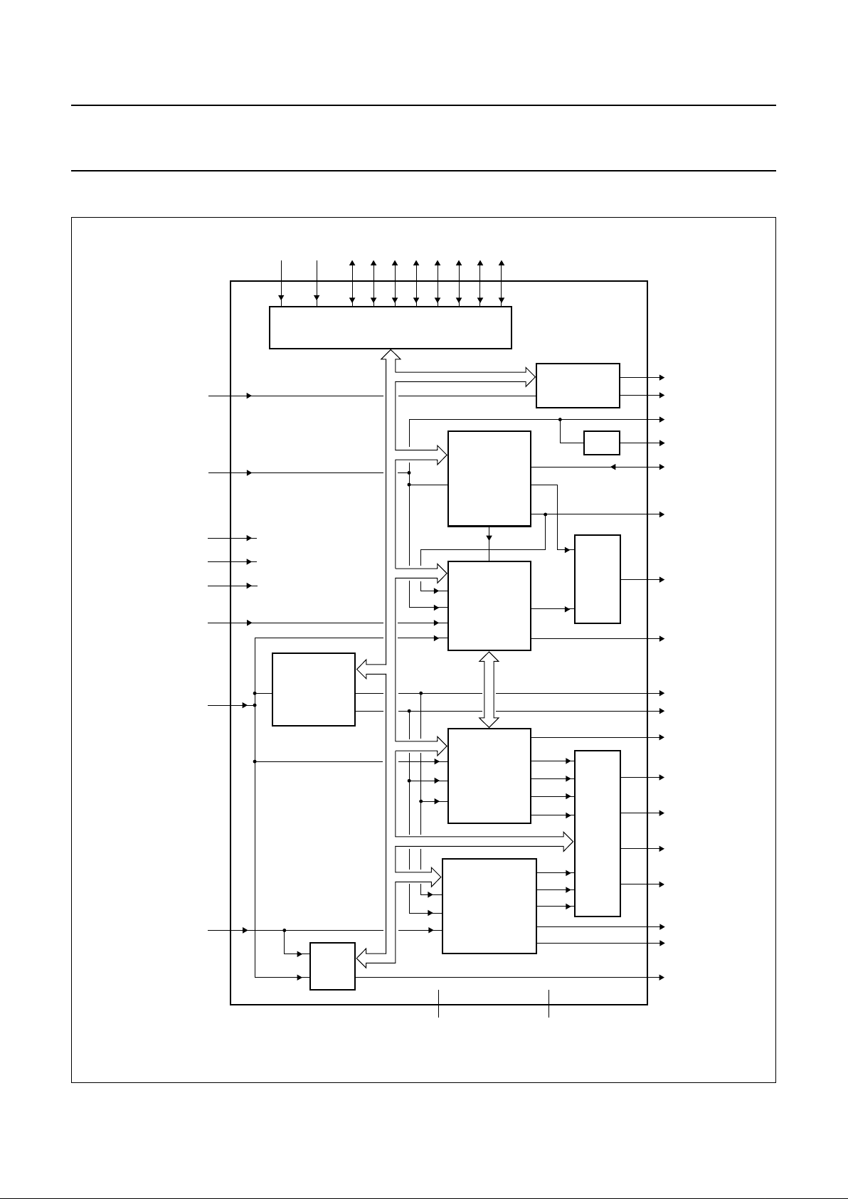
BLOCK DIAGRAM
Fig.1 Block diagram.
handbook, full pagewidth
MHA724
ALE
IE
PROCESSING
WRD P0 P1 P2
MICROCONTROLLER
INTERFACE
P3 P4 P5 P6 P7
÷ 2
LOGIC
STROBE
LLA
(12, 13.5, 16, 18 MHz)
TEST
SDP
SSC
VACQ
(50/60 Hz)
LLDFL
(27, 32, 36 MHz)
(32, 36 MHz)
LLD
VACQS
VWE2
HWE1
VWE1
VRE1
VRE2
VD
HWE2
HRE
HD
9
IE1
IE2
SWC1
SWC05
HRA/BLNA
CLV
WE1
RSTW1
HRDFL
HDFL
VDFL
BLND
HRD
SRC
21 22 25 26 27 28 29 30 31 32
7
SAA4952WP
14
3
6
11
16
8
42
35
37
38
20
1
RE2
19
RE1
18
HVCD
17
WE2
15
4
13
40
5
41
33
43
2, 10, 23, 36
39
ACQUISITION
HORIZONTAL
TIMING
ACQUISITION
VERTICAL
TIMING
DEFLECTION
TIMING
DISPLAY
VERTICAL
TIMING
DISPLAY
HORIZONTAL
TIMING
LOGIC
LOGIC
V
DD1
to V
DD4
V
SS1
to V
SS4
12, 24, 34, 44
Page 4

1997 Jun 10 4
Philips Semiconductors Objective specification
Memory controller SAA4952WP
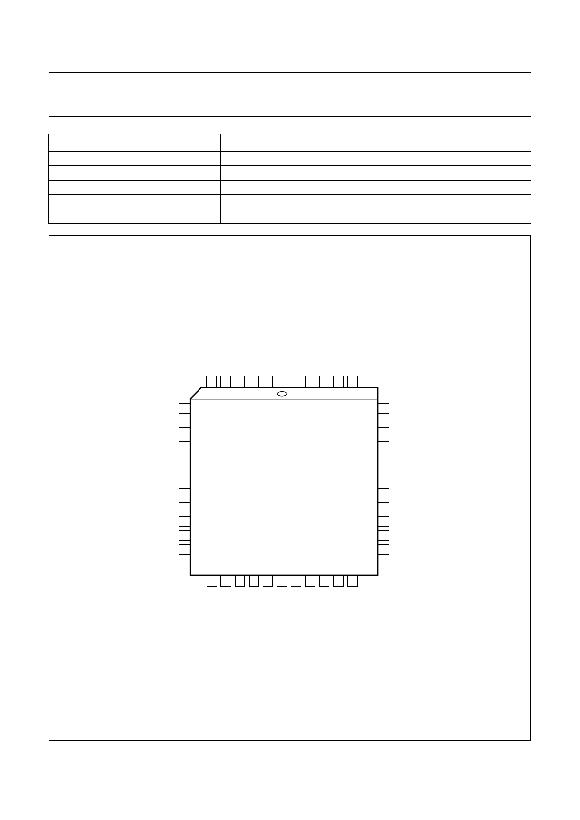
PINNING
SYMBOL PIN I/O DESCRIPTION
HRD 1 O horizontal reference signal output (display PLL)
V
DD1
2 supply supply voltage 1
SWC1 3 O serial write clock output for memory 1
SRC 4 O serial read clock output
SDP 5 I select deflection processor input
SWC05 6 O serial write clock output, SWC1 divided-by-2
IE1 7 O input enable signal output (memory 1)
WE1 8 O write enable signal output (memory 1)
STROBE 9 I strobe signal input
V
DD2
10 supply supply voltage 2
HRA/BLNA 11 I/O horizontal reference signal output (acquisition part)/horizontal blanking
signal input, reset for horizontal acquisition counters (acquisition part)
V
SS1
12 − ground 1
LLA 13 I line-locked clock signal input (acquisition part)
IE2 14 O input enable signal output (memory 2)
WE2 15 O write enable signal output (memory 2)
CLV 16 O horizontal signal output (acquisition part)
HVCD 17 O horizontal, vertical or composite blanking signal output (display part)
RE1 18 O read enable signal output (memory 1)
RE2 19 O read enable signal output (memory 2)
BLND 20 O horizontal blanking signal output (display part)
ALE 21 I address latch enable signal input
WRD 22 I write/read data signal input
V
DD3
23 supply supply voltage 3
V
SS2
24 − ground 2
P0 25 I/O data input/output signal bit 0
P1 26 I/O data input/output signal bit 1
P2 27 I/O data input/output signal bit 2
P3 28 I/O data input/output signal bit 3
P4 29 I/O data input/output signal bit 4
P5 30 I/O data input/output signal bit 5
P6 31 I/O data input/output signal bit 6
P7 32 I/O data input/output signal bit 7 (MSB = Most Significant Bit)
LLDFL 33 I line-locked clock signal input (deflection part)
V
SS3
34 − ground 3
HRDFL 35 O horizontal reference signal output (deflection part)
V
DD4
36 supply supply voltage 4
HDFL 37 O horizontal synchronization signal output (deflection part)
VDFL 38 O vertical synchronization signal output (deflection part)
VACQ 39 I vertical synchronization signal input (acquisition part)
Page 5
1997 Jun 10 5
Philips Semiconductors Objective specification
Memory controller SAA4952WP
TEST 40 I test input
SSC 41 I select single clock system input
RSTW1 42 O reset write signal output (memory 1)
LLD 43 I line-locked clock signal input (display part)
V
SS4
44 − ground 4
SYMBOL PIN I/O DESCRIPTION
Fig.2 Pin configuration.
handbook, full pagewidth
12
13
14
15
16
17
7
8
9
10
11
39
38
37
36
35
34
33
32
31
30
29
18
19
20
21
22
23
24
25
26
27
28
6
5
4
3
2
1
44
43
42
41
40
SAA4952WP
MHA723
VACQ
VDFL
HDFL
V
DD4
V
SS3
LLDFL
P7
P6
P5
P4
IE1
WE1
STROBE
V
DD2
HRA/BLNA
V
SS1
IE2
WE2
HVCD
HRDFL
SDP
SRC
SWC1
V
DD1
HRD
V
SS4
RSTW1
SSC
TEST
SWC05
LLD
RE2
BLND
ALE
WRD
V
DD3
V
SS2
P1
P2
P3
RE1
P0
LLA
CLV
Page 6

1997 Jun 10 6
Philips Semiconductors Objective specification
Memory controller SAA4952WP
FUNCTIONAL DESCRIPTION
The SAA4952WP is a memory controller intended to be
used for scan conversion in TV receivers. This conversion
is performed from 50 to 100 Hz or from 60 to 120 Hz.
Besides the doubling of the field frequency a progressive
scan conversion can be activated (50 Hz/1250 lines or
60 Hz/1050 lines). For low cost PALplus receivers a
simple 50 Hz/1fH mode can be performed. The device
supports up to three separate PLL circuits. The acquisition
PLL can operate with frequencies of 12, 13.5, 16 or
18 MHz. In a three-clock system the deflection PLL
operates with 27 MHz (see Fig.11). An additional display
PLL generates 32 or 36 MHz. If a two-clock system is
chosen the deflection PLL can operate with all possible
display frequencies (27, 32 and 36 MHz) and the extra
PLL can be omitted (see Fig.12). In a system using the
deflection processor TDA9151, three PLLs are necessary
because the 27 MHz clock is needed for the deflection.
If other deflection processors are used (e.g. TDA9152) two
PLLs are sufficient. The 50 Hz/1f
H
mode operates with a
single clock.
Frequency doubling is possible for input data rates of
12, 13.5, 16 and 18 MHz. Displaying a 4 : 3 picture on a
16 : 9 screen is possible by using the clock configuration
12/32 MHz and 13.5/36 MHz. A 14 : 9 picture can be
displayed on a 16 : 9 screen by the frequency
combinations 16/36 MHz or 12/32 MHz. The VCO and
loop filter are peripheral parts of each PLL, the clock
divider and generation of the reference pulse for the phase
detector are internally provided.
The device generates all write, read and clock pulses to
control a field memory in the desired mode. The required
signals are programmable via an 8-bit parallel
microcontroller port.
Figure 1 shows the block diagram of the SAA4952WP.
The clock signal LLA from the VCO is input at pin 13, a
horizontal reference pulse HRA for the phase discriminator
is output at pin 11. By setting the clock divider to different
values the PLL can be forced to operate with different
clock frequencies. The acquisition part can also be
configured to operate with an external clock frequency
from a digital source. Pin 11 is used as an input pin.
The horizontal reference pulse BLNA is supplied externally
to reset the horizontal counters. This mode is intended to
be used together with, for example, a digital colour
decoder which provides the clock and reference pulses.
The signals HWE1, CLV and HVACQS are generated in
the horizontal acquisition processing part. The vertical
processing block supplies the signals RSTW1 as well as a
vertical enable signal (VWE1) for the combined write
enable signal with a horizontal and vertical part (WE1).
The START and STOP position of the pulses are
programmable, whereas the increment equals 2 (4) clock
cycles in the horizontal part and 1 line in the vertical part.
For HWE1 an additional 2-bit fine delay is available.
Display related control signals are derived from the display
clock. The functions are similar to the acquisition part.
The clock frequency can be switched to 27, 32 or 36 MHz.
In the event of a three-clock system using the TDA9151
the 27 MHz clock frequency is generated by an additional
deflection PLL. In the horizontal part the pulses HWE2,
HR2, HD and BLND are programmable in increments of
2 (4) clock cycles, each one adjustable by an additional
2-bit fine delay. The vertical processing block generates
VDFL and enable signals for the horizontal part (VWE2,
VRE1, VRE2 and VD).
The 16 kHz PLL reference pulse HRDFL is generated from
the display clock frequencies (27, 32 or 36 MHz) and the
32 kHz deflection pulse HDFL. In the three-clock system
the deflection pulses are derived from an extra 27 MHz
clock, independent of the chosen mode of the scan
converter module.
The field length of two successive fields is measured in the
vertical acquisition part. The sampling of VACQ is
performed internally via the signal HVACQS, a pulse
which occurs every 32 µs. The position of this pulse is
programmable via the microcontroller interface to ensure
correct sampling of VACQ.
The measured length of the fields can be read by the
microcontroller. Depending on these values the
microcontroller selects an appropriate setting to achieve
an optimized display performance.
The 100 Hz vertical synchronizing signal VDFL is
generated in accordance with the measured length of the
incoming fields. The position towards the video data of this
pulse can also be selected by the microcontroller.
Furthermore two field identification signals for 50 Hz and
for 100 Hz are generated internally to mark the
corresponding display fields for the microcontroller.
The SAA4952WP supports two different Multi
Picture-In-Picture (MPIP) modes. In addition to the
features of the SAA4951WP the new controller is able to
generate a 3 × 3 MPIP without an external PIP module.
The PIP is obtained in a simple way by storing each third
pixel and line of the source into the memory. The display
is able to run free and is not synchronized to the PIP
source in this mode. One of the nine MPIPs can show a
live picture while the others are frozen.
Page 7

1997 Jun 10 7
Philips Semiconductors Objective specification
Memory controller SAA4952WP
By changing the active MPIP in a sequence all PIPs are
sequentially updated.
The second Multi-PIP option needs an extra PIP module.
This module produces a PIP picture which is originally
displayed at the bottom right position of the screen.
The information of the PIP picture is stored at a desired
position in the field memories. Depending on the
compression mode of the PIP module, the MPIP display
can be configured via software control
(e.g. 4 × 3, 4 × 4, etc.).
For basic features and PALplus systems a 50 Hz/1f
H
single clock mode is provided. Switching between a 2f
H
and the 1fH mode is performed by the SAA4952WP
hardware pin SHF to avoid wrong HDFL frequencies
which might occur in the event of a software controlled
selection. For the same reason the deflection processor is
selected via pin SDP, whereas in the case of the TDA9152
or another deflection processor without the need of a
constant 27 MHz clock, only two PLLs are necessary.
ICs from the new IC generation such as PALplus,
LIMERIC and PAN-IC need to be supplied with two clocks.
The frequency of one clock equals the frequency of the
output data (13.5, 16 or 18 MHz). A second clock operates
with twice the frequency (27, 32 or 36 MHz).
The SAA4952WP generates the necessary signals,
whereas SWC05 is obtained by dividing LLA by a factor of
two.
The display section can be set into a fixed mode via the
microcontroller port. This allows a generator mode
function for displaying OSD without a stable input signal.
A still picture can be shown on the screen completely
decoupled from the input of the converter. The generator
mode can also be used if the MPIP function is activated.
Microcontroller interface
The SAA4952WP is connected to a microcontroller via
pins P0 to P7, ALE and WRD. This controller receives
commands from the I
2
C-bus and sets the register of the
SAA4952WP accordingly. Figure 3 shows the timing of
these signals. Address and data are transmitted
sequentially on the bus with the falling edge of ALE
denoting a valid address and the falling edge of WRD
denoting valid data. The individual registers, their address
and their function are listed in Tables 1 to 12. Various
START and STOP registers are 9 bits wide, in this
instance the MSB is combined with MSBs of other signals
or fine delay control bits in an extra control register which
has to be addressed and loaded separately.
In order to load the proper values to the vertical control
registers (VWE2, VRE1 and VRE2) in the event of e.g.
median filtering, information about the current 100 Hz field
is necessary. To obtain this data, the microcontroller
sends the address 80H (read mode) which puts the
SAA4952WP in output mode for the next address/data
cycle. For this one cycle the WRD pin works as a RDN pin.
The microcontroller is able to read the length of the
incoming fields. The length is measured in multiples of
32 µs. The result of the measurement is a 10-bit data
word. The first 8 bits can be accessed under read address
81H. Register 80H contains the MSB and the 9th bit.
The exact knowledge of the field length makes it possible
to decide in which standard the input signal was
transmitted. The microcontroller is able to detect
non-standard sources such as a VCR in trick modes. It is
also possible to decide whether the input is interlaced or
non-interlaced. The vertical control signals to the
memories are adapted to the source to obtain a stable
display.
Fig.3 Microcontroller interface timing.
handbook, full pagewidth
MGH133
ALE
WRD
DATA
ADDRESS
ADDRESS
ADDRESS
DATA
DATA
Page 8
1997 Jun 10 8
Philips Semiconductors Objective specification
Memory controller SAA4952WP
Internal registers
Table 1 Vertical display related pulses
Notes
1. VDFLSTA, VDFLSTO, SETFIELD1 and SETFIELD2 are programmable in increments of half lines (16 µs/32 µs).
2. The memory control signals VWE2, VRE1 and VRE2 as well as VD can be changed in steps of one display line.
ADDRESS
(HEX)
REGISTER FUNCTION
40 VDFLSTA
(1)
start of VDFL pulse (only 8-bit)
41 VDFLSTO
(1)
stop of VDFL pulse (only 8-bit)
42 VWE2STA
(2)
start of vertical write enable 2 (lower 8 of 9 bits)
43 VWE2STO
(2)
stop of vertical write enable 2 (lower 8 of 9 bits)
44 VRE2STA
(2)
start of vertical read enable 2 (lower 8 of 9 bits)
45 VRE2STO
(2)
stop of vertical read enable 2 (lower 8 of 9 bits)
46 VRE1STA
(2)
start of vertical read enable 1 (lower 8 of 9 bits)
47 VRE1STO
(2)
stop of vertical read enable 1 (lower 8 of 9 bits)
53 VDSTA
(2)
start of vertical display signal (lower 8 of 9 bits)
54 VDSTO
(2)
stop of vertical display signal (lower 8 of 9 bits)
55 VDMSB
(2)
bit 0: MSB of VRE1STA
bit 1: MSB of VRE1STO
bit 2: MSB of VWE2STA
bit 3: MSB of VWE2STO
bit 4: MSB of VRE2STA
bit 5: MSB of VRE2STO
bit 6: MSB of VDSTA
bit 7: MSB of VDSTO
62 SETFIELD1
(1)
field length to be set by the microcontroller in the generator mode (lower 8 of 10 bits);
bit 0 = LSB
63 SETFIELD2
(1)
field length to be set by the microcontroller in the generator mode;
bit 0: bit 8 of field length
bit 1: bit 9 of field length (MSB)
Page 9
1997 Jun 10 9
Philips Semiconductors Objective specification
Memory controller SAA4952WP
Table 2 Horizontal display related pulses
ADDRESS
(HEX)
REGISTER FUNCTION
48 BLNDSTA start of horizontal blanking pulse (lower 8 of 9 bits)
49 BLNDSTO stop of horizontal blanking pulse (lower 8 of 9 bits)
4A HWE2STA start of horizontal write enable 2 (lower 8 of 9 bits)
4B HWE2STO stop of horizontal write enable 2 (lower 8 of 9 bits)
4C HRESTA start of horizontal read enable (lower 8 of 9 bits)
4D HRESTO stop of horizontal read enable (lower 8 of 9 bits)
56 HDSTA start of horizontal display signal HD (lower 8 of 9 bits)
57 HDSTO stop of horizontal display signal HD (lower 8 of 9 bits)
4E HDMSB bit 0: MSB of BLNDSTA
bit 1: MSB of BLNDSTO
bit 2: MSB of HWE2STA
bit 3: MSB of HWE2STO
bit 4: MSB of HRESTA
bit 5: MSB of HRESTO
bit 6: MSB of HDSTA
bit 7: MSB of HDSTO
4F HDDEL bit 0: fine delay of BLND (LSB)
bit 1: fine delay of BLND (MSB)
bit 2: fine delay of HWE2 (LSB)
bit 3: fine delay of HWE2 (MSB)
bit 4: fine delay of HRE (LSB)
bit 5: fine delay of HRE (MSB)
bit 6: fine delay of HD (LSB)
bit 7: fine delay of HD (MSB)
64 HVSP1 horizontal pulse 1 for frame synchronization, 8-bit resolution
65 HVSP2 horizontal pulse 2 for frame synchronization, 8-bit resolution
66 HVSP3 horizontal pulse 3 for frame synchronization, 8-bit resolution
67 HVSP4 horizontal pulse 4 for frame synchronization, 8-bit resolution
Page 10

1997 Jun 10 10
Philips Semiconductors Objective specification
Memory controller SAA4952WP
Table 3 Vertical acquisition related pulses
Note
1. VWE1 programmable in steps of 1 line (64 µs).
ADDRESS
(HEX)
REGISTER FUNCTION
50 VWE1STA
(1)
start of vertical write enable (lower 8 of 9 bits)
51 VWE1STO
(1)
stop of vertical write enable (lower 8 of 9 bits)
52 VAMSB bit 0: MSB of VWE1STA
bit 1: MSB of VWE1STO
bit 2:
BRE = 0: normal operation
BRE = 1: RE output is blanking every second line in program scan mode
bit 3:
BWE = 0: normal operation
BWE = 1: WE2 output is blanking every second line in program scan mode
bit 4: BPRR: Blanking Phase Relation RE for program
BPRR = 0: AND connection HRDFL and HRE
BPRR = 1: AND connection HRDFLN and HRE
bit 5: BPRW: Blanking Phase Relation WE2 for program
BPRW = 0: AND connection HRDFL and HWE2
BPRW = 1: AND connection HRDFLN and HWE2
bit 6: BVRA: Blanking Vertical Reset Acquisition
BVRA = 0: reset blanking disabled
BVRA = 1: reset blanking enabled
bit 7: BVRD: Blanking Vertical Reset Display
BVRD = 0: reset blanking disabled
BVRD = 1: reset blanking enabled
Page 11

1997 Jun 10 11
Philips Semiconductors Objective specification
Memory controller SAA4952WP
Table 4 Horizontal acquisition related pulses
Table 5 Mode registers
Table 6 Read registers
ADDRESS
(HEX)
REGISTER FUNCTION
58 CLVSTA start of clamp pulse
59 CLVSTO stop of clamp pulse
5A HWE1STA start of horizontal write enable 1 (lower 8 of 9 bits)
5B HWE1STO stop of horizontal write enable 1 (lower 8 of 9 bits)
5C HAMSBDEL bit 0: MSB of HWE1STA
bit 1: MSB of HWE1STO
bit 2: fine delay of HWE1 (LSB)
bit 3: fine delay of HWE1 (MSB)
bit 4: PWC05: Phase of Write Clock SWC05, determines the phase relationship of
SWC05 towards BLNA or HRA
bit 5: SFR: Select Field Recognition mode
bit 6: FRD: Field Recognition Disabled (FRD = 1)
bit 7: don’t care
5D HVACQS1 VACQ sample pulse 1
5E HVACQS2 VACQ sample pulse 2
ADDRESS
(HEX)
REGISTER FUNCTION
60 MODE0 mode register 0; see Table 7
61 MODE1 mode register 1; see Table 10
ADDRESS
(HEX)
REGISTER FUNCTION
81 FIELDINF2 bit 0: bit 8 of field length measurement
bit 1: bit 9 of field length measurement (MSB)
bit 2: LSB of display field count
bit 3: field recognition for incoming source
bit 4: MSB of display field count
80 FIELDINF1 result of field length measurement (lower 8 of 10 bits)
Page 12

1997 Jun 10 12
Philips Semiconductors Objective specification
Memory controller SAA4952WP
Table 7 Mode0 register description
Table 8 Acquisition frequency
Table 9 Display frequency
REGISTER BIT NAME REMARKS
MODE0 0 (LSB) FSA0 frequency select acquisition 0; see Table 8
1 FSA1 frequency select acquisition 1; see Table 8
2 FSD0 frequency select display 0; see Table 9
3 FSD1 frequency select display 1; see Table 9
4 SDAF select doubled acquisition frequency
SDAF = 0: normal operation
SDAF = 1: doubled acquisition frequency (2f
a
)
5 IMPIP MPIP select bit
IMPIP = 0: normal operation
IMPIP = 1: MPIP mode active
6 INPIP number of PIPs
INPIP = 0: 3 × 3 MPIP
INPIP = 1: 4 × 4 MPIP
7 GMOD generator mode for display
GMOD = 0: normal operation
GMOD = 1: generator mode for display; field length measurement is
disabled
FSA1 FSA0 FREQUENCY (MHz)
0 0 12.0
0 1 13.5
1 0 16.0
1 1 18.0
FSD1 FSD0 FREQUENCY (MHz)
0 0 27.0
0 1 27.0
1 0 32.0
1 1 36.0
Page 13

1997 Jun 10 13
Philips Semiconductors Objective specification
Memory controller SAA4952WP
Table 10 Mode1 register description
Table 11 Signal mode at pin 17
Table 12 Display modes
Notes
1. VFS: Vertical Frequency Select; register MODE1; bit 7.
2. SSC: Select Single Clock SAA4952WP input pin 41.
3. DR: Display Raster; register MODE1; bit 0.
REGISTER BIT NAME REMARKS
MODE1 0 DR display raster
1 STPWM1 stop writing to memory 1; still picture mode; STROBE signal can override still
picture mode
2 STPWM2 stop writing to memory 2; still picture mode
3 SD0 select mode of display signal at pin 17; bit 0
4 GSC golden SCART mode
GSC = 0: normal operation
GSC = 1: golden SCART mode
5 SD1 select mode of display signal at pin 17; bit 1; see Table 11
6 EXTLLA external acquisition clock
EXTLLA = 0: normal operation
EXTLLA = 1: LLA and horizontal reference pulse BLNA (horizontal reset)
from external digital source
7 VFS vertical frequency select
VFS = 0: 100/120 Hz
VFS = 1: 50/60 Hz
SD1 SD0 MODE
0 0 horizontal signal HD at the output
0 1 vertical signal VD at the output
1 0 composite signal CD (derived from HD and VD by AND connection) at the output
1 1 composite signal CD at the output
CONTROL BITS
DISPLAY MODE (NUMBER OF LINES VALID FOR STANDARD PAL)
VFS
(1)
SSC
(2)
DR
(3)
0 0 0 100 Hz (312.5 lines) ABAB raster
0 0 1 100 Hz (313, 312.5, 312 and 312.5 lines) AABB raster
0 1 0 not allowed
0 1 1 not allowed
1 0 0 50 Hz (625 lines) 1 : 1; non-interlaced
1 0 1 50 Hz (1250 lines) 2 : 1; interlaced
1 1 0 50 Hz (312.5 lines) 2 : 1
1 1 1 not allowed
Page 14

1997 Jun 10 14
Philips Semiconductors Objective specification
Memory controller SAA4952WP
Description of the acquisition part
LLA
This is the main input clock pulse for the acquisition part of
the memory controller normally generated by an external
PLL circuit. Depending on the chosen system application
LLA operates on the different frequencies of 12, 13.5, 16
and 18 MHz. When SDAF = 1 these frequencies are
doubled to 24, 27, 32 and 36 MHz. The PLL circuit is
controlled by the Analog Burst Key pulse (ABK) provided
by an inserted synchronization circuit (i.e. TDA2579 or
TDA9141) and the horizontal reference signal (HRA)
supplied by the SAA4952WP.
SWC1
The acquisition clock input signal LLA is connected via the
memory controller circuit SAA4952WP. LLA is internally
buffered and output as serial write clock for memory 1.
Additionally SWC1 is used as a clock signal for the
analog-to-digital converter (e.g. TDA8755).
SWC05
The signal SWC05 is obtained by dividing the clock LLA by
a factor of two. SWC05 is needed for feature concepts
containing new IC generations such as PALplus, LIMERIC
or PAN-IC.
HRA/BLNA
The horizontal reference output pulse (HRA) is used as the
digital feedback pulse for the phase comparator of the
acquisition PLL. The duty cycle of the signal is 50%.
The positive edge of HRA indicates the internal counter
reset.
When the memory controller operates in a digital
environment, a horizontal reference signal (BLNA) and a
suitable acquisition clock pulse have to be supplied from
the externally used circuits (i.e. SAA7151A, DMSD and
SAA7157, CGC). The rising edge of BLNA resets the
internal horizontal acquisition counters of the
SAA4952WP.
CLV
The horizontal video clamping output pulse is generated
by the acquisition clock signal LLA and can be used as a
clamp pulse for the incoming luminance and chrominance
signals Y, U and V for the analog-to-digital converter.
The time reference of CLV is the LOW-to-HIGH transition
of the HRA signal. In comparison to the SAA4951WP the
signal CLV has no internal influence on the vertical
processing and is free programmable.
WE1
A HIGH level on this output pin enables picture data to be
written to field memory 1. WE1 is a composite signal,
which includes the horizontal write enable signal (HWE1)
and the vertical write enable signal (VWE1). The position
of HWE1 can be programmed without restrictions.
It is possible to delay the horizontal timing of WE1 by up to
three LLA clock cycles. WE1 operates at a vertical
frequency of 50/60 Hz.
IE1
This output signal is used as a data input enable for
memory 1. A logic HIGH level on this output pin enables
the data information to be written into field memory 1.
The still picture function is controlled via signal IE1. When
this mode is selected, IE1 is switched to a LOW level. It is
possible to disable the still picture mode with externally
supplied STROBE pulses. Using this function a live PIP
insertion into a frozen main picture is possible, as the write
pointer of memory 1 is still incremented, depending on the
level of WE1. The STROBE input is not sampled in the
controller. This means that the display part of the PIP
module should be synchronized to the IPQ write clock.
HVACQS
The vertical synchronization signal for the acquisition part
(VACQ) is sampled by the pulse HVACQS twice per line.
This signal consists of the two programmable pulses
HVACQS1 and HVACQS2 (see Fig.4). To ensure a save,
sampling the position of each pulse (two per line) can be
programmed in steps of four LLA clock cycles. The signal
is referenced to the rising edge of HRA.
Page 15

1997 Jun 10 15
Philips Semiconductors Objective specification
Memory controller SAA4952WP
Table 13 Horizontal programming range of CLV, HWE1 and HVACQS
Nr (programmed start value of corresponding signal) not equal Nf (programmed stop value of corresponding signal).
Notes
1. N: programmed value of HVACQS1 pulse.
2. M: programmed value of HVACQS2 pulse.
The programmed values include the MSB setting contained in HAMSBDEL.
For SDAF = 1 the factors in front of Nr and Nf are doubled.
For EXTLLA = 1 the equations for LLA = 18 MHz are valid.
The programming margins depend on the used external clock frequency.
ACQUISITION FREQUENCY
(MHz)
TIMING EQUATIONS PROGRAMMING RANGE
12 CLV
r
= (4Nr + 2)LLA 0 ≤ Nr < 191
CLV
f
= (4Nf + 2)LLA 0 ≤ Nf < 191
HWE1
r
= (2Nr + 2)LLA 0 ≤ Nr < 383
HWE1
f
= (2Nf + 2)LLA 0 ≤ Nf < 383
HVACQS1 = (4N
(1)
+ 2)LLA 0 ≤ N < 191
HVACQS2 = (4M
(2)
+ 2)LLA 0 ≤ M < 191
13.5 CLV
r
= (4Nr + 2)LLA 0 ≤ Nr < 215
CLV
f
= (4Nf + 2)LLA 0 ≤ Nf < 215
HWE1
r
= (2Nr + 2)LLA 0 ≤ Nr < 431
HWE1
f
= (2Nf + 2)LLA 0 ≤ Nf < 431
HVACQS1 = (4N
(1)
+ 2)LLA 0 ≤ N < 215
HVACQS2 = (4M
(2)
+ 2)LLA 0 ≤ M < 215
16 CLV
r
= (4Nr + 2)LLA 0 ≤ Nr < 255
CLV
f
= (4Nf + 2)LLA 0 ≤ Nf < 255
HWE1
r
= (2Nr + 2)LLA 0 ≤ Nr < 511
HWE1
f
= (2Nf + 2)LLA 0 ≤ Nf < 511
HVACQS1 = (4N
(1)
+ 2)LLA 0 ≤ N < 255
HVACQS2 = (4M
(2)
+ 2)LLA 0 ≤ M < 255
18 CLV
r
= (8Nr + 2)LLA 0 ≤ Nr < 143
CLV
f
= (8Nf + 2)LLA 0 ≤ Nf < 143
HWE1
r
= (4Nr + 2)LLA 0 ≤ Nr < 287
HWE1
f
= (4Nf + 2)LLA 0 ≤ Nf < 287
HVACQS1 = (8N
(1)
+ 2)LLA 0 ≤ N < 143
HVACQS2 = (8M
(2)
+ 2)LLA 0 ≤ M < 143
1
LLAEXT
----------------------
N× 64 µs≤
Page 16

1997 Jun 10 16
Philips Semiconductors Objective specification
Memory controller SAA4952WP
VACQ
This is the 50 Hz vertical synchronization input signal
derived from a suitable vertical synchronization circuit
(i.e. TDA2579). The LOW-to-HIGH transition of this pulse
is the timing reference of all vertical control signals of the
SAA4952WP.
The vertical acquisition timing is illustrated in Fig.5. VWE1
is resynchronized with HWE1 internally. Nr and Nf can
represent values varying between 1 and 511, whereas Nf
should be programmed in accordance with the expected
field length (PAL 312, NTSC 262). If the incoming fields
are shorter than programmed the memory controller resets
VWE1 itself.
RSTW1
The reset write output pulse 1 starts the write address
pointer of field memory 1. The RSTW1 signal is derived
from the 50 Hz vertical acquisition pulse (VACQ) and has
a pulse width of 32 µs.
STROBE
The asynchronous, active HIGH, STROBE input controls
the input enable signal IE1 to memory 1 in the still picture
mode (see Section “IE1”).
Display and deflection part
LLD
The input signal LLD is a line-locked clock for the display
side of the memory controller.
In the event of a two-clock system the possible display
frequencies (27, 32 and 36 MHz) are derived from one
switchable external PLL. The internal system clocks LLD is
supplied via the input LLDFL. The input pin LLD is not used
and its level can be fixed. This configuration is foreseen for
applications using the TDA9152 or other deflection
controllers which do not need a clock supply.
In applications using the TDA9151 a 27 MHz clock is
always required. The system has to operate in a
three-clock mode. The deflection PLL generates the
27 MHz clock frequency only, whereas the display PLL
generates the 32 and 36 MHz in parallel, if conversion
modes are used which operate with these display
frequencies. If the display is operating with 27 MHz, LLD is
switched to the deflection PLL input and the third PLL can
be omitted. The 32 and 36 MHz PLL is synchronized on
the horizontal deflection pulse (HDFL). A digital feedback
signal (HRD) to the phase comparator is supplied by the
memory controller.
In the 50 Hz/1f
H
mode only one system clock is required.
The display, deflection and acquisition clocks are equal.
SRC
The display clock input signal from inputs LLD or LLDFL is
buffered in the memory controller. Depending on the
selected mode one of them is output as Serial Read Clock
(SRC) for the field memories. Additionally SRC is used as
a clock pulse for the writing of memory 2, the noise
reduction circuit NORIC and the back-end circuit BENDIC
or for PROZONIC (instead of NORIC) and the following
DAC.
HRD
The Horizontal Reference Display pulse (HRD) has a duty
cycle of 50% and a frequency of 32 kHz. HRD is the
reference pulse for the horizontal timing of the control
signals RE1, RE2, WE2, HD and BLND generated by the
display part of the SAA4952WP in the event of a
three-clock system with a selected display frequency of
32 or 36 MHz.
HVSP
The vertical display counter is incremented with every
HVSP pulse (see Fig.6). The HVSP signal is created from
the four pulses HVSP1 to HVSP4. The distance between
the pulses has to be programmed to 16 µs. The HVSP
signal is the equivalent to the HVACQS signal of the
vertical acquisition part. The HVSP1 pulse should be
programmed 32 µs after the HVACQS1 pulse. This
programming ensures that the vertical picture stability is
also kept in the event of unstable sources such as VCRs.
BLND
The output signal BLND is a horizontal blanking pulse and
is, for example, used for the peripheral circuits NORIC and
BENDIC. A LOW level indicates the blanking interval, a
HIGH level indicates valid data from the memories. It is
possible to delay the horizontal timing of BLND by up to
three LLD clock pulses.
WE2
A HIGH level on this output pin enables picture data to be
written to field memory 2. WE2 is a composite signal which
includes the horizontal write enable signal and the vertical
write enable signal. The horizontal timing of WE2 can be
delayed by up to three steps of LLD clock pulses.
Page 17

1997 Jun 10 17
Philips Semiconductors Objective specification
Memory controller SAA4952WP
HVCD
The memory controller supplies a display related output
which can generate, depending on the microcontroller
initialization, three different signals. The desired mode is
activated via microcontroller register MODE1 (control bits
SD0 and SD1).
Table 14 Mode setting of SAA4952WP output HVCD
IE2
This output signal is used as data input enable for
memory 2. A logic HIGH level on this output pin enables
the data information to be written to field memory 2.
SD1 SD0 MODE OF OUTPUT PIN 17
0 0 horizontal output signal HD; programmable
via HDSTA and HDSTO
0 1 vertical output signal VD; programmable via
VDSTA and VDSTO
1 X composite output signal HVCD; logical
AND connection of HD and VD
RE1
The output RE1 is the read enable signal for field
memory 1. A HIGH level enables the picture data to be
read from the memory. RE1 is a composite signal and
includes the horizontal read enable timing (HRE) and the
vertical read enable timing (VRE). It is possible to delay the
horizontal timing of RE1 by up to three display clock
pulses. The horizontal timing of RE1 and RE2 is equal.
RE2
The output RE2 is the read enable signal for field
memory 2. A HIGH level enables the picture data to be
read from memory. RE2 is a composite signal and includes
the horizontal read enable timing (HRE) and the vertical
read enable timing (VRE2). The horizontal timing of RE2
can be delayed by up to three display clock pulses.
The new memory controller supplies two completely
independent VRE signals, VRE1 and VRE2. VRE1 is not
generated as an adjustable delay of VRE2 as in the
SAA4951WP.
Table 15 Programming range of horizontal display signals (BLND, HRE, HWE2, HD and HVSP1 to HVSP4); see Fig.6
Nr (programmed start (rise) value of corresponding signal) not equal Nf (programmed stop (fall) value of corresponding
signal).
Notes
1. HVSP
n
= HVSP1 to HVSP4.
2. N: programmed value of HVSP pulse.
LLD equals LLDFL for 27 MHz display in the three-clock system.
LLD input is not used in the two-clock mode (internally switched to LLDFL input).
The programmed values include the MSB settings contained in HDMSB.
ACQUISITION FREQUENCY
(MHz)
TIMING EQUATIONS PROGRAMMING RANGE
27 HDSPr= (2Nr + 2)LLD 0 ≤ Nr < 431
HDSP
f
= (2Nf + 2)LLD 0 ≤ Nf < 431
HVSP
n
(1)
= (4N
(2)
+ 2)LLD 0 ≤ N < 215
32 HDSP
r
= (2Nr + 2)LLD 0 ≤ Nr < 511
HDSP
f
= (2Nf + 2)LLD 0 ≤ Nf < 511
HVSP
n
(1)
= (4N
(2)
+ 2)LLD 0 ≤ N < 255
36 HDSP
r
= (4Nr + 4)LLD 0 ≤ Nr < 287
HDSP
f
= (4Nf + 4)LLD 0 ≤ Nf < 287
HVSP
n
(1)
= (8N
(2)
+ 4)LLD 0 ≤ N < 145
Page 18

1997 Jun 10 18
Philips Semiconductors Objective specification
Memory controller SAA4952WP
The vertical display signal can be programmed in a range
of Nr, Nf from 1 to 511. The setting should correspond to
the source (PAL, NTSC) and the expected standard field
length. For the display the vertical read window should not
exceed the write window. In the event of non-standard
sources with shortened field lengths the memory controller
disables the vertical control signals if the programmed
STOP setting cannot be reached.
LLDFL
The input signal LLDFL is the main line-locked clock pulse
for the display and deflection part generated by an external
PLL circuit. The frequency of LLDFL is 27, 32 or 36 MHz
for a two-clock system. It is fixed to 27 MHz if the
three-clock system is chosen. In this mode, display clocks
of 32 and 36 MHz are generated by an extra display PLL.
The PLL circuit operates on the burst key pulse (ABK) of
the acquisition part and the horizontal reference signal
HRDFL generated by the deflection part of the memory
controller.
The LLDFL should not fall below 24 MHz because this
clock is used to sample the input signals at the memory
controller port (P0 to P7), ALE and WRD.
HRDFL
This horizontal output signal is the reference pulse for the
horizontal deflection drive signal HDFL. The duty cycle of
HRDFL is 50% and the cycle time is 64 µs (PAL). For the
golden SCART mode the cycle time is reduced to 32 µs.
VDFL
This is the vertical synchronization output signal generated
by the vertical deflection part of the memory controller.
The timing reference of VDFL is the LOW-to-HIGH
transition of the vertical acquisition input pulse VACQ.
Normally VDFL has a pulse width of 2.5 × HDFL = 80 µs
and a cycle time of 100 Hz.
HDFL
The output signal HDFL is used for driving the connected
horizontal deflection circuit. HDFL has a cycle time of
32 µs and a pulse width of 64 × LLDFL = 2.37 µs in the 2f
H
mode (see Fig.8).
Control inputs and outputs
ALE
The address latch enable input signal ALE is provided by
the microcontroller. A falling edge of ALE denotes a valid
address.
WRD
This is the write/read enable control signal supplied by the
microcontroller. The HIGH-to-LOW transition of WRD
indicates valid data.
P0
TO P7
The SAA4952WP is controlled by the bidirectional parallel
port bus P0 to P7 of a microcontroller. Address and data
are transmitted sequentially on the parallel bus.
TEST
The TEST input pin has to be connected to ground.
SDP
The SDP input pin has to be connected to ground for a
three-clock system. This configuration has to be chosen if
the TDA9151 is controlling the deflection. Connecting SDP
to the supply voltage switches the memory controller into
the two-clock mode.
Table 16 SDP mode pin setting
SSC
The Select Single Clock (SSC) control pin has to be
connected to ground to activate a 2fHmode and a multi
clock system. For the 50 Hz/1fH mode in a single clock
system the input is connected to the supply (VDD).
Table 17 SCC mode pin setting
TIMING SPECIFICATION
The internal delays of the output signals referenced to the
respective clock are given in Table 18.
SDP REMARK
0 three-clock system; supports TDA9151
1 two-clock system
SCC REMARK
02f
H
mode (100/120 Hz; progressive scan);
two-clock or three-clock system
11f
H
mode (50/60 Hz; 15.625/15.75 kHz);
single clock system
Page 19

1997 Jun 10 19
Philips Semiconductors Objective specification
Memory controller SAA4952WP
Table 18 Delay table (see Fig.9)
Worst case conditions: V
DD
= 4.5 V and T
amb
=85°C. Typical case conditions: VDD= 5 V and T
amb
=25°C.
Note
1. Source for SRC depends on the setting of register MODE0 and the level on the SDP pin.
CLK OUTPUT
LOAD
(pF)
t
h(min)
(ns)
t
h(typ)
(ns)
t
pd(max)
(ns)
t
pd(typ)
(ns)
LLA SWC1 15 2 3 11 8
LLA SWC05 15 4 5 13 10
LLD SRC 45 3 4 10 8
LLDFL
(1)
SRC 45 3 4 10 8
LLA WE1 15 7 8 18 13
LLD WE2 10 7 8 18 13
LLD RE1 10 8 9 18 13
LLD RE2 10 7 7 18 13
LLDFL HDFL 25 7 7 12 10
LLD BLND 25 8 9 19 13
LLD HVCD 25 8 8 20 15
LLA CLV 25 7 8 12 10
LLDFL VDFL 25 7 7 12 9
Fig.4 Horizontal acquisition timing.
handbook, full pagewidth
MHA725
HRA
CLV
f
CLV
r
CLV
HWE1
HVACQS
HWE1
r
HWE1
f
HVACQS1
HVACQS2
Page 20

1997 Jun 10 20
Philips Semiconductors Objective specification
Memory controller SAA4952WP
Fig.5 Vertical acquisition timing.
(1) Vr(WE1) =Nr × line.
(2) Vf(WE1) = Nf × line.
handbook, full pagewidth
MHA726
VACQ
VWE1
Vr(WE1)
(1)
Vf(WE1)
(2)
RSTW1
Fig.6 Programmable horizontal display signals.
(1) HDSP = BLND, HRE and HWE2.
(2) HVSP consists of the 4 pulses HVSP1 to HVSP4 (HVSPn).
handbook, full pagewidth
MHA727
HRD or
HRDFL
HDSP
(1)
HVSP
(2)
HDSP
r
HVSP
n
(2)
HDSP
f
Page 21

1997 Jun 10 21
Philips Semiconductors Objective specification
Memory controller SAA4952WP
Fig.7 Vertical display timing [VDSP = V(WE2) and V(RE1/2)].
handbook, full pagewidth
MHA728
VACQ
VDSP
RSTW2
VDSP
r
VDSP
f
Fig.8 Horizontal deflection timing (example for 27 MHz).
handbook, full pagewidth
MHA729
HRDFL
HDFL
64 × LLDFL 64 × LLDFL
1728 × LLDFL
864 × LLDFL
Page 22

1997 Jun 10 22
Philips Semiconductors Objective specification
Memory controller SAA4952WP
LIMITING VALUES
In accordance with the Absolute Maximum Rating System (IEC 134).
THERMAL CHARACTERISTICS
SYMBOL PARAMETER MIN. MAX. UNIT
V
DD
supply voltage −0.5 +6.0 V
V
i
input voltage −0.5 VDD+ 0.5 V
f
clk
clock frequency − 38 MHz
T
stg
storage temperature −40 +125 °C
T
amb
operating ambient temperature 0 85 °C
SYMBOL PARAMETER VALUE UNIT
R
th j-c
thermal resistance from junction to case 46 K/W
Fig.9 Timing diagram.
handbook, full pagewidth
MHA733
CLK
OUTPUT
t
h
t
pd
Page 23

1997 Jun 10 23
Philips Semiconductors Objective specification
Memory controller SAA4952WP
CHARACTERISTICS
V
DD
=5V; T
amb
=25°C; unless otherwise specified.
Notes
1. f
min
= 24 MHz for LLDFL, if the data at the microcontroller port P0 to P7, ALE and WRD is supplied from a
microcontroller clocked with 12 MHz.
2. For SRC Io= ±8 mA.
SYMBOL PARAMETER CONDITIONS MIN. TYP. MAX. UNIT
V
DD
supply voltage 4.5 5 5.5 V
I
DD
supply current − 35 − mA
f
acq
acquisition frequency −−33 MHz
f
LLDFL,LLD
operating frequency of display and deflection part note 1 24 − 37 MHz
C
i
input capacitance − 10 15 pF
V
IL
LOW level input voltage −−0.8 V
V
IH
HIGH level input voltage 2.0 −−V
V
OL
LOW level output voltage Io= 4 mA; note 2 −−0.4 V
V
OH
HIGH level output voltage Io= −4 mA; note 2 2.4 3.4 − V
T
j
junction temperature −−125 °C
T
amb
operating ambient temperature 0 − 85 °C
APPLICATION INFORMATION
Figure 10 illustrates a block diagram of the application
environment of the memory controller SAA4952WP.
The full option chip set of the new TV feature system
controlled by the I2C-bus includes the following circuits:
TDA8755
ADC.
SAA4955TJ
3 Mbit video RAM.
SAA4995WP
PANorama-IC (PAN-IC) for linear horizontal zoom and
compression, non-linear (panorama) horizontal aspect
ratio conversion.
SAA7165
VEDA2, DAC with digital CTI and luminance peaking.
SAA4990H
Progressive scan-Zoom and Noise reduction IC
(PROZONIC) with line flicker reduction.
SAA4991WP
The Motion Estimation/Compensation Line flicker
reduction ZOom and Noise reduction IC is abbreviated as
MELZONIC.
SAA4952WP
Memory controller.
S87C654-4A44
Microcontroller.
Page 24

1997 Jun 10 24
Philips Semiconductors Objective specification
Memory controller SAA4952WP
Application diagrams
book, full pagewidth
MHA730
ADC
CLV
RSTR
SWC1
VEDA2
SAA7165
VIDEO
ENHANCED
DAC
CTI, PEAKING
PROGRESSIVE
SCAN, LFR,
VERTICAL ZOOM,
NOISE
REDUCTION
CROSS-COLOUR
REDUCTION
PROZONIC
SAA4990H
MEMORY BLOCK
2 × SAA4955TJ
MEMORY CONTROLLER
SAA4952WP
YUV
3
TDA8755
12
2
24
RE1 output
RE2 output
WE2
24
12
3
YUV
V
H
DEFLECTION
TDA9151
VDFL
HDFL
LLDFL
27 MHz
MICRO-
CONTROLLER
P83C652/4FBA
21,22
25 to 32
38
37
9
39
11 13
16 3 7 8 42 14 15 1942018
143 35 33
CLV
SWC1
IE1
WE1
RSTW1
IE2
SRC
RE1
HVCD
HRA HRD HRDFL LLDFLLLD
ALE, WRD
P0 to P7
I
2
C-bus
I
2
C-bus
VDFL
STROBE
VACQ
ABK
SNERT-bus
COMP
LLA
CLV
HDFL
12, 13.5, 16
18 MHz
32, 36 MHz 27 MHz
PD
VCO
PD
VCO
PD
VCO
acquisition display deflection
Fig.10 Application diagram.
Page 25

1997 Jun 10 25
Philips Semiconductors Objective specification
Memory controller SAA4952WP
d
book, full pagewidth
MHA731
LPF
FEATURE CONNECTOR
ADC
TDA8755
PAN-IC
MEMORY 1
1 ×
SAA4955TJ
SAA4995WP
LPF
LPF
VCO1
I
2
C-bus
I2C-bus
VCO2
SNERT-bus
Y
12
U
V
HA, VA
12
12
MEMORY 2
1 ×
SAA4955TJ
MEMORY
CONTROLLER
SAA4952WP
MICROCONTROLLER
S87C654
12
f
A
f
D
12
VEDA2
SAA7165
CTI
Y-PEAKING
DAC
VERTICAL ZOOM
LINE FLICKER
REDUCTION
NOISE AND
CROSS-COLOUR
REDUCTION
PROZONIC
SAA4990H
12
Y
U
video processor
TDA4780
RGB output stages
TDA6111
V
HD, VD
to
deflection
processor
12
12
2
CONTROL DATA
8
CONTROL
Fig.11 Block diagram of a full-options IPQ module MK6.
Page 26

1997 Jun 10 26
Philips Semiconductors Objective specification
Memory controller SAA4952WP
b
ook, full pagewidth
MHA732
LPF
FEATURE CONNECTOR
ADC
TDA8755
PAN-IC
MEMORY 1
1 ×
SAA4955TJ
SAA4995WP
LPF
LPF
VCO1 VCO2
Y
12
U
V
HA, VA
12
12
MEMORY 2
1 ×
SAA4955TJ
MEMORY
CONTROLLER
SAA4952WP
MICROCONTROLLER
S87C654
12
f
A
f
D
12
VEDA2
SAA7165
CTI
Y-PEAKING
DAC
MOTION ESTIMATION
AND COMPENSATION
LINE FLICKER
REDUCTION
NOISE AND
CROSS-COLOUR
REDUCTION
VERTICAL ZOOM
MELZONIC
SAA4991WP
12
Y
U
video processor
TDA4780
RGB output stages
TDA6111
V
HD, VD
to
deflection
processor
12
12
2
CONTROL DATA
8
CONTROL
I2C-bus
I2C-bus
SNERT-bus
Fig.12 Block diagram of a full-options IPQ module MK7.
Page 27

1997 Jun 10 27
Philips Semiconductors Objective specification
Memory controller SAA4952WP
PACKAGE OUTLINE
UNIT A
A
min. max. max. max. max.
1
A
4
b
p
E
(1)
(1) (1)
eH
E
Z
ywv β
REFERENCES
OUTLINE
VERSION
EUROPEAN
PROJECTION
ISSUE DATE
IEC JEDEC EIAJ
mm
4.57
4.19
0.51
3.05
0.53
0.33
0.021
0.013
16.66
16.51
1.27
17.65
17.40
0.51
2.16
45
o
0.18 0.100.18
DIMENSIONS (millimetre dimensions are derived from the original inch dimensions)
Note
1. Plastic or metal protrusions of 0.01 inches maximum per side are not included.
SOT187-2
D
(1)
16.66
16.51
H
D
17.65
17.40
E
Z
2.16
D
b
1
0.81
0.66
k
1.22
1.07
k
1
0.180
0.165
0.020
0.12
A
3
0.25
0.01
0.656
0.650
0.05
0.695
0.685
0.020
0.085
0.007 0.0040.007
L
p
1.44
1.02
0.057
0.040
0.656
0.650
0.695
0.685
e
E
e
D
16.00
14.99
0.630
0.590
16.00
14.99
0.630
0.590
0.085
0.032
0.026
0.048
0.042
2939
44
1
6
717
28
18
40
detail X
(A )
3
b
p
w M
A
1
A
A
4
L
p
b
1
β
k
1
k
X
y
e
E
B
D
H
E
e
E
H
v M
B
D
Z
D
A
Z
E
e
v M
A
pin 1 index
112E10 MO-047AC
0 5 10 mm
scale
92-11-17
95-02-25
inches
PLCC44: plastic leaded chip carrier; 44 leads
SOT187-2
D
e
Page 28

1997 Jun 10 28
Philips Semiconductors Objective specification
Memory controller SAA4952WP
SOLDERING
Introduction
There is no soldering method that is ideal for all IC
packages. Wave soldering is often preferred when
through-hole and surface mounted components are mixed
on one printed-circuit board. However, wave soldering is
not always suitable for surface mounted ICs, or for
printed-circuits with high population densities. In these
situations reflow soldering is often used.
This text gives a very brief insight to a complex technology.
A more in-depth account of soldering ICs can be found in
our
“IC Package Databook”
(order code 9398 652 90011).
Reflow soldering
Reflow soldering techniques are suitable for all PLCC
packages.
The choice of heating method may be influenced by larger
PLCC packages (44 leads, or more). If infrared or vapour
phase heating is used and the large packages are not
absolutely dry (less than 0.1% moisture content by
weight), vaporization of the small amount of moisture in
them can cause cracking of the plastic body. For more
information, refer to the Drypack chapter in our
“Quality
Reference Handbook”
(order code 9398 510 63011).
Reflow soldering requires solder paste (a suspension of
fine solder particles, flux and binding agent) to be applied
to the printed-circuit board by screen printing, stencilling or
pressure-syringe dispensing before package placement.
Several techniques exist for reflowing; for example,
thermal conduction by heated belt. Dwell times vary
between 50 and 300 seconds depending on heating
method. Typical reflow temperatures range from
215 to 250 °C.
Preheating is necessary to dry the paste and evaporate
the binding agent. Preheating duration: 45 minutes at
45 °C.
Wave soldering
Wave soldering techniques can be used for all PLCC
packages if the following conditions are observed:
• A double-wave (a turbulent wave with high upward
pressure followed by a smooth laminar wave) soldering
technique should be used.
• The longitudinal axis of the package footprint must be
parallel to the solder flow.
• The package footprint must incorporate solder thieves at
the downstream corners.
During placement and before soldering, the package must
be fixed with a droplet of adhesive. The adhesive can be
applied by screen printing, pin transfer or syringe
dispensing. The package can be soldered after the
adhesive is cured.
Maximum permissible solder temperature is 260 °C, and
maximum duration of package immersion in solder is
10 seconds, if cooled to less than 150 °C within
6 seconds. Typical dwell time is 4 seconds at 250 °C.
A mildly-activated flux will eliminate the need for removal
of corrosive residues in most applications.
Repairing soldered joints
Fix the component by first soldering two diagonallyopposite end leads. Use only a low voltage soldering iron
(less than 24 V) applied to the flat part of the lead. Contact
time must be limited to 10 seconds at up to 300 °C. When
using a dedicated tool, all other leads can be soldered in
one operation within 2 to 5 seconds between
270 and 320 °C.
Page 29

1997 Jun 10 29
Philips Semiconductors Objective specification
Memory controller SAA4952WP
DEFINITIONS
LIFE SUPPORT APPLICATIONS
These products are not designed for use in life support appliances, devices, or systems where malfunction of these
products can reasonably be expected to result in personal injury. Philips customers using or selling these products for
use in such applications do so at their own risk and agree to fully indemnify Philips for any damages resulting from such
improper use or sale.
Data sheet status
Objective specification This data sheet contains target or goal specifications for product development.
Preliminary specification This data sheet contains preliminary data; supplementary data may be published later.
Product specification This data sheet contains final product specifications.
Limiting values
Limiting values given are in accordance with the Absolute Maximum Rating System (IEC 134). Stress above one or
more of the limiting values may cause permanent damage to the device. These are stress ratings only and operation
of the device at these or at any other conditions above those given in the Characteristics sections of the specification
is not implied. Exposure to limiting values for extended periods may affect device reliability.
Application information
Where application information is given, it is advisory and does not form part of the specification.
Page 30

1997 Jun 10 30
Philips Semiconductors Objective specification
Memory controller SAA4952WP
NOTES
Page 31

1997 Jun 10 31
Philips Semiconductors Objective specification
Memory controller SAA4952WP
NOTES
Page 32

Internet: http://www.semiconductors.philips.com
Philips Semiconductors – a worldwide company
© Philips Electronics N.V. 1997 SCA54
All rights are reserved. Reproduction in whole or in part is prohibited without the prior written consent of the copyright owner.
The information presented in this document does not form part of any quotation or contract, is believed to be accurate and reliable and may be changed
without notice. No liability will be accepted by the publisher for any consequence of its use. Publication thereof does not convey nor imply any license
under patent- or other industrial or intellectual property rights.
Netherlands: Postbus 90050, 5600 PB EINDHOVEN, Bldg. VB,
Tel. +31 40 27 82785, Fax. +31 40 27 88399
New Zealand: 2 Wagener Place, C.P.O. Box 1041, AUCKLAND,
Tel. +64 9 849 4160, Fax. +64 9 849 7811
Norway: Box 1, Manglerud 0612, OSLO,
Tel. +47 22 74 8000, Fax. +47 22 74 8341
Philippines: Philips Semiconductors Philippines Inc.,
106 Valero St. Salcedo Village, P.O. Box 2108 MCC, MAKATI,
Metro MANILA, Tel. +63 2 816 6380, Fax. +63 2 817 3474
Poland: Ul. Lukiska 10, PL 04-123 WARSZAWA,
Tel. +48 22 612 2831, Fax. +48 22 612 2327
Portugal: see Spain
Romania: see Italy
Russia: Philips Russia, Ul. Usatcheva 35A, 119048 MOSCOW,
Tel. +7 095 755 6918, Fax. +7 095 755 6919
Singapore: Lorong 1, Toa Payoh, SINGAPORE 1231,
Tel. +65 350 2538, Fax. +65 251 6500
Slovakia: see Austria
Slovenia: see Italy
South Africa: S.A. PHILIPS Pty Ltd., 195-215 Main Road Martindale,
2092 JOHANNESBURG, P.O. Box 7430 Johannesburg 2000,
Tel. +27 11 470 5911, Fax. +27 11 470 5494
South America: Rua do Rocio 220, 5th floor, Suite 51,
04552-903 São Paulo, SÃO PAULO - SP, Brazil,
Tel. +55 11 821 2333, Fax. +55 11 829 1849
Spain: Balmes 22, 08007 BARCELONA,
Tel. +34 3 301 6312, Fax. +34 3 301 4107
Sweden: Kottbygatan 7, Akalla, S-16485 STOCKHOLM,
Tel. +46 8 632 2000, Fax. +46 8 632 2745
Switzerland: Allmendstrasse 140, CH-8027 ZÜRICH,
Tel. +41 1 488 2686, Fax. +41 1 481 7730
Taiwan: Philips Semiconductors, 6F, No. 96, Chien Kuo N. Rd., Sec. 1,
TAIPEI, Taiwan Tel. +886 2 2134 2865, Fax. +886 2 2134 2874
Thailand: PHILIPS ELECTRONICS (THAILAND) Ltd.,
209/2 Sanpavuth-Bangna Road Prakanong, BANGKOK 10260,
Tel. +66 2 745 4090, Fax. +66 2 398 0793
Turkey: Talatpasa Cad. No. 5, 80640 GÜLTEPE/ISTANBUL,
Tel. +90 212 279 2770, Fax. +90 212 282 6707
Ukraine: PHILIPS UKRAINE, 4 Patrice Lumumba str., Building B, Floor 7,
252042 KIEV, Tel. +380 44 264 2776, Fax. +380 44 268 0461
United Kingdom: Philips Semiconductors Ltd., 276 Bath Road, Hayes,
MIDDLESEX UB3 5BX, Tel. +44 181 730 5000, Fax. +44 181 754 8421
United States: 811 East Arques Avenue, SUNNYVALE, CA 94088-3409,
Tel. +1 800 234 7381
Uruguay: see South America
Vietnam: see Singapore
Yugoslavia: PHILIPS, Trg N. Pasica 5/v, 11000 BEOGRAD,
Tel. +381 11 625 344, Fax.+381 11 635 777
For all other countries apply to: Philips Semiconductors, Marketing & Sales Communications,
Building BE-p, P.O. Box 218, 5600 MD EINDHOVEN, The Netherlands, Fax. +31 40 27 24825
Argentina: see South America
Australia: 34 Waterloo Road, NORTH RYDE, NSW 2113,
Tel. +61 2 9805 4455, Fax. +61 2 9805 4466
Austria: Computerstr. 6, A-1101 WIEN, P.O. Box 213,
Tel. +43 1 60 101, Fax. +43 1 60 101 1210
Belarus: Hotel Minsk Business Center, Bld. 3, r. 1211, Volodarski Str. 6,
220050 MINSK, Tel. +375 172 200 733, Fax. +375 172 200 773
Belgium: see The Netherlands
Brazil: see South America
Bulgaria: Philips Bulgaria Ltd., Energoproject, 15th floor,
51 James Bourchier Blvd., 1407 SOFIA,
Tel. +359 2 689 211, Fax. +359 2 689 102
Canada: PHILIPS SEMICONDUCTORS/COMPONENTS,
Tel. +1 800 234 7381
China/Hong Kong: 501 Hong Kong Industrial Technology Centre,
72 Tat Chee Avenue, Kowloon Tong, HONG KONG,
Tel. +852 2319 7888, Fax. +852 2319 7700
Colombia: see South America
Czech Republic: see Austria
Denmark: Prags Boulevard 80, PB 1919, DK-2300 COPENHAGEN S,
Tel. +45 32 88 2636, Fax. +45 31 57 0044
Finland: Sinikalliontie 3, FIN-02630 ESPOO,
Tel. +358 9 615800, Fax. +358 9 61580920
France: 4 Rue du Port-aux-Vins, BP317, 92156 SURESNES Cedex,
Tel. +33 1 40 99 6161, Fax. +33 1 40 99 6427
Germany: Hammerbrookstraße 69, D-20097 HAMBURG,
Tel. +49 40 23 53 60, Fax. +49 40 23 536 300
Greece: No. 15, 25th March Street, GR 17778 TAVROS/ATHENS,
Tel. +30 1 4894 339/239, Fax. +30 1 4814 240
Hungary: see Austria
India: Philips INDIA Ltd, Shivsagar Estate, A Block, Dr. Annie Besant Rd.
Worli, MUMBAI 400 018, Tel. +91 22 4938 541, Fax. +91 22 4938 722
Indonesia: see Singapore
Ireland: Newstead, Clonskeagh, DUBLIN 14,
Tel. +353 1 7640 000, Fax. +353 1 7640 200
Israel: RAPAC Electronics, 7 Kehilat Saloniki St, PO Box 18053,
TEL AVIV 61180, Tel. +972 3 645 0444, Fax. +972 3 649 1007
Italy: PHILIPS SEMICONDUCTORS, Piazza IV Novembre 3,
20124 MILANO, Tel. +39 2 6752 2531, Fax. +39 2 6752 2557
Japan: Philips Bldg 13-37, Kohnan 2-chome, Minato-ku, TOKYO 108,
Tel. +81 3 3740 5130, Fax. +81 3 3740 5077
Korea: Philips House, 260-199 Itaewon-dong, Yongsan-ku, SEOUL,
Tel. +82 2 709 1412, Fax. +82 2 709 1415
Malaysia: No. 76 Jalan Universiti, 46200 PETALING JAYA, SELANGOR,
Tel. +60 3 750 5214, Fax. +60 3 757 4880
Mexico: 5900 Gateway East, Suite 200, EL PASO, TEXAS 79905,
Tel. +9-5 800 234 7381
Middle East: see Italy
Printed in The Netherlands 547047/20/01/pp32 Date of release: 1997 Jun 10 Document order number: 9397 750 01973
 Loading...