

Page 1

INTEGRATED CIRCUITS
DATA SH EET
SAA2521
Masking threshold processor for
MPEG layer 1 audio compression
applications
Preliminary specification
File under Integrated Circuits, IC01
August 1993
Page 2

Philips Semiconductors Preliminary specification
Masking threshold processor for MPEG
SAA2521
layer 1 audio compression applications
FEATURES
• Stereo or 2-channel mono encoding
• Status may be read continuously
• Microcontroller interface
• I2S-interfaces
• Allocation algorithm including optional emphasis
correction (for 44.1 kHz)
• Reduced power consumption
• 4 V nominal operating voltage capability.
ORDERING INFORMATION
EXTENDED TYPE
NUMBER
SAA2521GP 44 QFP plastic SOT205AG
Note
1. SOT205-1; 1996 August 23.
PINS PIN POSITION MATERIAL CODE
GENERAL DESCRIPTION
The SAA2521 performs the adaptive allocation and
scaling function for calculating the masking thresholds and
sub-band sample accuracy in MPEG layer 1 applications.
The SAA2521 is intended for use in conjunction with the
stereo filter codec SAA2520.
PACKAGE
(1)
August 1993 2
Page 3

Philips Semiconductors Preliminary specification
Masking threshold processor for MPEG
layer 1 audio compression applications
handbook, full pagewidth
SWS
FS256
FDAF
NODONE
RESOL0
RESOL1
FDIR
FRESET
FSYNC
SCALE
TEST3
TEST4
31
39
34
INTERFACE INTERFACECOMPENSATION DELAY
20
21
22
37
36
35
38
15
16
CONTROL
SAA2521
ALLOCATION AND
SCALING
CALCULATION
V
DD
14,24,40
SAA2521
33
FDAC
32
SCL
LTDATA
LTCNT1
LTCNT0
LTENA
LTCLK
CLK24
RESET
PWRDWN
5
1
2
3
4
26
23
30
LT INTERFACE
6,25,44
V
SS
11
7
8
9
10
MLB137
LTDATAC
LTCNT1C
LTCNT0C
LTENC
LTCLKC
Fig.1 Block diagram.
August 1993 3
Page 4

Philips Semiconductors Preliminary specification
Masking threshold processor for MPEG
layer 1 audio compression applications
SS
V
n.c.
n.c.
handbook, full pagewidth
LTCNT1
LTCNT0
LTENA
LTCLK
LTDATA
V
SS
LTCNT1C
LTCNT0C
LTENC
LTCLKC
LTDATAC
44
1
2
3
4
5
6
7
8
9
10
11
n.c.
43
42
41
SAA2521
SAA2521
DD
V
40
FS256
39
SCALE
38
FDIR
37
FRESET
FSYNC
36
35
FDAF
34
33
32
31
30
29
28
27
26
25
24
23
FDAC
SCL
SWS
PWRDWN
TEST10
TEST9
TEST8
CLK24
V
SS
V
DD
RESET
handbook, full pagewidth
AUDIO
SOURCE
MICROCONTROLLER
AMPLIFIER
ADC/DAC
AUDIO
digital audio interface
system micro interface
12
13
14
15
16
17
DD
V
TEST1
TEST2
TEST3
TEST4
TEST5
Fig.2 Pin configuration.
control
power down
reset
18
19
TEST6
TEST7
SAA2520
and
SAA2521
21
20
RESOL0
NODONE
22
MLB136
RESOL1
MPEG interface
MPEG
source/
receiver
MLB138
Fig.3 MPEG codec system data flow diagram.
August 1993 4
Page 5

Philips Semiconductors Preliminary specification
Masking threshold processor for MPEG
SAA2521
layer 1 audio compression applications
PINNING
SYMBOL PIN DESCRIPTION TYPE
LTCNT1 1 mode control 1, microcontroller interface input I
LTCNT0 2 mode control 0, microcontroller interface input I
LTENA 3 enable microcontroller interface input I
LTCLK 4 bit clock microcontroller interface input I
LTDATA 5 data, microcontroller interface (3-state inputs/outputs) I/O
V
SS
LTCNT1C 7 control 1; microcomputer interface O
LTCNT0C 8 control 0; microcomputer interface O
LTENC 9 enable microcontroller interface O
LTCLKC 10 bit clock; microcontroller interface O
LTDATAC 11 data; microcontroller interface, (3-state inputs/outputs) I/O
TEST1 12 test output; do not connect
TEST2 13 test output; do not connect
V
DD
TEST3 15 test mode input; to be connected to V
TEST4 16 test mode input; to be connected to V
TEST5 17 test input; to be connected to V
TEST6 18 test input; to be connected to V
TEST7 19 test input; to be connected to V
NODONE 20 no done state selection input I
RESOL0 21 resolution selection 0 input I
RESOL1 22 resolution selection 1 input I
RESET 23 active HIGH reset input I
V
DD
V
SS
CLK24 26 24.576 MHz processing clock input I
TEST8 27 test input; to be connected to V
TEST9 28 test input; to be connected to V
TEST10 29 test input; to be connected to V
PWRDWN 30 power-down input I
SWS 31 word selection input; (Filtered) - I
SCL 32 bit clock input; (Filtered) - I
FDAC 33 filtered data (Filtered) - I
FDAF 34 filtered data (Filtered) - I
FSYNC 35 sub-band synchronization on (Filtered) - I
FRESET 36 reset signal input from SAA2520 I
FDIR 37 direction of the I
SCALE 38 scale factor index select (note 1) I
FS256 39 system clock input; sample frequency × 256 I
V
DD
6 supply ground (0 V)
14 positive supply voltage (+ 5 V)
24 positive supply voltage (+ 5 V)
25 supply ground (0 V)
2
S-interface I
2
S-interface (3-state inputs/outputs) I/O
2
S-interface (3-state inputs/outputs) I/O
2
S-interface; input I
40 positive supply voltage (+ 5 V)
DD
DD
SS
SS
SS
SS
SS
SS
2
S-interface I
2
S-interface, input I
August 1993 5
Page 6

Philips Semiconductors Preliminary specification
Masking threshold processor for MPEG
SAA2521
layer 1 audio compression applications
SYMBOL PIN DESCRIPTION TYPE
n.c. 41 not connected
n.c. 42 not connected
n.c. 43 not connected
V
SS
Note to the Pinning Description
1. The scale input must be set LOW for use with the SAA2521.
FUNCTIONAL DESCRIPTION
Coding System
This efficient MPEG audio encoder is used in conjunction
with the SAA2520 filter codec (bit rates of 384, 256, 192
and 128 k bits/s). The encoder utilizes a system producing
sub-band samples from an incoming digital audio signal.
This relies upon the audibility of signals above a given
level and upon high amplitude signals masking those of
lower amplitude. Although each sub-band signal is of
approximately 750 Hz bandwidth, it possesses
considerable overlap with those adjacent to it.
During the process of encoding, the masking threshold
processor analyses the broadband audio signal at
sampling frequency f
signals at a sampling frequency (fs/32).
The coded signal consists of frames conveying the
information corresponding to the sub-band samples.
These also include a synchronization pattern identifying
the start of each new frame. The allocation information for
the 32 sub-bands is transferred as 4-bit values. If the
amplitude of a sub-band signal is below the masking
threshold it will be omitted from the coded signal.
The duration of a MPEG frame depends upon sampling
frequency and is adjusted to 384 divided by fs.
44 supply ground (0 V)
by splitting it into 32 sub-band
s
Encoding Mode
Signal FDIR sets the data flow direction on the
Filtered-I
the device will accept samples from FDAF. These will be
delayed by a number of sample periods depending upon
the setting of the SCALE input. In the instance of operation
with the SAA2520 (SCALE = logic 0) this delay will be 480
SWS periods. This will ensure alignment of the data with
the computed allocations.
After the delay the samples will be presented on FDAC
(pin 33). The circuit also performs all the calculations
required to build the allocation table which is used in the
codec (SAA2520). When used with the SAA2520 the
calculated scale factor indices are sent via the LT
interface. These operations are performed for every frame
of the sub-band codec.
In order to synchronize with the codec and utilize the
correct tables for the calculations the SAA2521 frequently
requests the status of the codec. It monitors the bit-rate,
sample frequency, operation mode and the emphasis
information and uses the 'ready to receive' bit of the codec
to determine the moment of the transfer of allocation
information.
Decoding Mode
2
S-interface. In the encoding mode (FDIR LOW)
Adaptive Allocation and Scaling
The coding system calculates the masking power of the
sub-band signals and adds the masking threshold.
Sub-band signals with power below this threshold denote
information to be discarded. Non-masked signals are
coded using floating point notation in which a mantissa
corresponds in length to the difference between peak
power and masking threshold. The process is repeated for
every MPEG frame and is known as the Adaptive
Allocation of the available capacity.
August 1993 6
In the decoding mode (FDIR HIGH) the SAA2521 will take
samples from FDAC which will be presented on the FDAF
after a delay of 160 SWS periods. The LT interface
between microcontroller and codec (SAA2520) will only be
affected by the 'ready to receive' bit from the codec
(SAA2520).
Page 7

Philips Semiconductors Preliminary specification
Masking threshold processor for MPEG
layer 1 audio compression applications
Microcontroller Interface Operation
Information on the interface between microcontroller and
codec (SAA2520) will flow in a regular sequence
synchronized with the codec (SAA2520):
- with every FSYNC the SAA2521 will read the status of
the codec (SAA2520)
- Following the calculation of the allocation and scale
factors the SAA2521 will send the first allocation
information unit (16-bits). It will then continuously read
the codec (SAA2520) status to ascertain when it is
able to receive further allocation information units.
When the transfer of these units is complete the
SAA2521 will send settings and (for SCALE = logic 0)
scale factor indices.
- The extended settings will be sent to the codec as
soon as possible after reception from the
microcontroller.
The microcontroller communicates with the SAA2521 in
a similar fashion:
- status can be read continuously. The SAA2521 will
output a copy of the codec (SAA2520) status on the
LTDATA line except for the 'ready to receive' bits
which are generated by the SAA2521. These indicate
whether the SAA2521 is ready to receive the next
settings or extended settings.
- settings can be sent following every occasion that the
'ready to receive' bit 'S' changes to logic 1.
- extended settings can be sent following each
occasion that the 'ready to receive' bit 'E' changes to
logic 1.
SAA2521
Mode Control
Operation is controlled by the FRESET and FDIR signals.
FRESET causes a general reset. The FDIR signal is
sampled at the falling edge of the FRESET signal to
determine the operation mode:
FDIR = logic 1 decoding mode, SAA2521 in
feed-through mode
FDIR = 0 encoding mode, SAA2521 in
calculation mode
Fig.4 shows the timing diagram for FRESET and FDIR.
Resolution Selection
The (SAA2521) is designed for operation with input
devices (ADCs) which may possess a different sample
resolution capability, i.e. audio sample inputs into the
sub-band filters. Pins RESOL0 and RESOL1 (respectively
pins 21 and 22) may be utilized to adjust the allocation
information calculation to the resolution of the samples.
With the instance of pin 20 (NODONE) being HIGH, all
available bits in the bit-pool will be allocated. If NODONE
is LOW, no bits will be allocated to the sub-bands with
energy levels below the theoretical threshold for the
selected resolution.
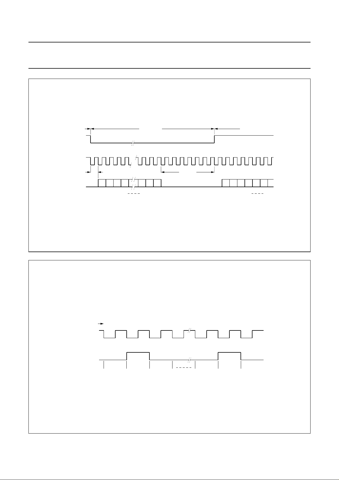
t
FRESET
t
suD
FDIR
TrH> 5T
TsD < 0 ns min. set-up time FDIR to FRESET = LOW
= 210 ns (for CLK24 = 24.576 MHz) min. time FRESET HIGH
CLK24
Fig.4 Timing: FRESET and FDIR.
August 1993 7
rH
MBC123 - 1
Page 8

Philips Semiconductors Preliminary specification
Masking threshold processor for MPEG
layer 1 audio compression applications
Power-down Mode Switching
When the potential on the RESET pin (pin 23) is held HIGH
for at least 5T
after which it will operate in its decoding mode.
The power-down mode is activated when the PWRDWN
pin (pin 30) is held HIGH. The 3-state buffers will be set to
a high impedance while the normal outputs will retain the
state attained prior to this mode being entered. This mode
can only be used if other associated circuits react
accordingly. The power-down mode is de-activated by a
reset action.
Fig.5 shows the operation for the power-down mode
switching.
clock periods, the device will be reset
CLK24
SAA2521
Table 1 Resolution selection.
RESOL1 RESOL0 RESOLUTION
0 0 16-bits
0 1 18-bits
1 0 14-bits
1 1 15-bits
TrH> 5T
PWRDWN
RESET
= 210 ns (for CLK24 = 24.576 MHz) minimum time RESET HIGH
CLK24
Fig.5 Power-down mode switching.
sleep mode active
t
rH
MEA659 - 1
August 1993 8
Page 9
Philips Semiconductors Preliminary specification
Masking threshold processor for MPEG
layer 1 audio compression applications
channel
SWS
SCL
FDA
bit :
1
0
msb lsb
left 32 bits
2102322212
7 bits
2322212
msb
right
0
SAA2521
MBC149 - 1
channel
SWS
FSYNC
sub-band
Fig.6 Format for transferring filtered data.
LRLLLLLLRRRRRR
31 0 1 31 0 1
MBC126 - 2
Fig.7 FSYNC related to SWS 0 data transfer period.
August 1993 9
Page 10

Philips Semiconductors Preliminary specification
Masking threshold processor for MPEG
layer 1 audio compression applications
Table 2 The (Filtered) - I2S-interface.
SWS input word selection F
SCL input bit clock 64 F
FDAF bi-directional filtered data to/from the filter section of SAA2520
FDAC bi-directional filtered data to/from the codec section of SAA2520
FSYNC input filter synchronization F
2
Table 3 The (Filtered) - I
FRESET input reset
FDIR input Filtered - I
(Filtered) - I2S-interfaces
Interfaces with the sub-band filter and codec (SAA2520)
consist of the following signals.
Fig.6 shows the format for transferring filtered data.
Fs256 must be provided as system clock. This frequency
is used by the interfaces with the SAA2520.
S-interface.
2
S-interface direction of data flow
SAA2521
s
s
/32
s
The frequency of the SWS signal (pin 31) is equal to the
sample frequency Fs. Bit clock SCL (pin 32) is 64 times the
sample frequency; thus each SWS period contains 64 data
bits, 48 of which are actually used in data transfer. The half
period during which SWS is logic 0 is used to transfer
Left-channel information while that during which it is 1
permits transfer of Right-channel data.
The 24-bit samples are transferred with the most
significant bit first. This bit is transferred during the bit clock
period, one bit time after the change in SWS.
FSYNC signal is provided for the purposes of
synchronization and indicates the portion of the SWS
period during which the samples of sub-band 0 are
transferred.
Fig.7 shows the relationship between FSYNC and the
SWS 0 data transfer period.
August 1993 10
Page 11

Philips Semiconductors Preliminary specification
Masking threshold processor for MPEG
layer 1 audio compression applications
4T
t
cH
SCL
t
d4
output
input
t
d3
SAA2521
t
cL
t
su1
t
h1
MBC127 - 2
OUTPUT applies to FDAF and FDAC in the output mode.
INPUT applies to FDAF and FDAC in the input mode, SWS and FSYNC.
T = one Fs256 cycle time
tcH ≥ T +35 ns minimum HIGH time SCL
TcL≥ T +35 ns minimum LOW time SCL
td3≥ 2T − 10 ns hold time output after SCL HIGH
td4≤ 3T +60 ns delay time output after SCL HIGH
ts1≥ 20 ns set-up time input before SCL HIGH
th1≥ T +35 ns hold time input after SCL HIGH
FDIR
t
W1
FDA
HIGH Z HIGH Z
t
W2
MEA692 - 1
tw1≥ 3T minimum time high impedance to FDA enabled
tw2 ≥ 2T +35 ns maximum time FDA enabled to high impedance
Fig.8 (Filtered) - I2S-interface timing.
August 1993 11
Page 12

Philips Semiconductors Preliminary specification
Masking threshold processor for MPEG
SAA2521
layer 1 audio compression applications
Table 4 SAA2521 interface with microcontroller.
LTCLK input bitclock
LTDATA bi-directional data
LTCNT0 input control line 0
LTCNT1 input control line 1
LTENA input enable
Table 6 SAA2521 interface control lines functions.
LTCNT1(C) LTCNT0(C) MODE FROM TO TRANSFER OF
0 0 extended settings microcontroller SAA2520 8-bits
0 1 allocation (see note) SAA2521 SAA2520 16/48 × 16-bits
1 0 settings microcontroller SAA2520 16-bits
1 1 status codec microcontroller 8 or 16-bits
Microcontroller Interface
Two microcontroller interfaces are provided; one for
connection to the microcontroller interface of the
SAA2520, the other to connect to the system controller.
Information is conveyed via the SAA2521 which executes
monitoring and extracts signals (e.g. settings and
synchronization) essential to its operation. Additionally it
also sends allocation information to the SAA2520.
However, the SAA2521 does not monitor the external
settings bits from the microcontroller (see Extended
Settings).
Table 5 SAA2521 interface with SAA2520.
LTCLKC output bit clock
LTDATAC bi-directional data
LTCNT0C output control line 0
LTCNT1C output control line 1
LTENC output enable
A transfer of information begins when the master sets the
control lines for the required action. It then sets the
LTENA/C line to logic 1. Once this signal is established the
slave determines the kind of action required and prepares
for the transfer of data.
When the master supplies the LTCLK/C signal, data is
transferred either to or from the slave in units of 8-bits; the
least significant bit is always transferred first. A transfer of
16-bits is made in two, 8-bit units with the most significant
8-bit unit first. In between the two 8-bit units the LTENA/C
signal remains logic 1.
The SAA2521 is a slave on the interface with the
microcontroller which is active only when the enable signal
LTENA (pin 3) is logic 1. This permits connection of this
interface to other devices. Only the enable signal is not
common to all devices.
SAA2521 is master on the interface with the SAA2520 and
provides all signals with the exception of the data in the
instance of status transfer from SAA2520 to SAA2521.
Information conveyed via these interfaces is transferred in
8 or 16-bit serial units with the type of information
designated by the control lines (LTCNT1(C) and
LTCNT0(C)).
Fig.9 shows an example of information transfer via
SAA2521 interfaces.
Note to Table 6
This mode only on the interface between SAA2521 and
SAA2520.
If SCALE = logic 1 then 16 × 16-bits
If SCALE = logic 0 then 48 × 16-bits
August 1993 12
Page 13

Philips Semiconductors Preliminary specification
Masking threshold processor for MPEG
layer 1 audio compression applications
LTENA/C
LTCNT0(C)/1(C)
LTCLK(C)
LTDATA(C)
01234567
SAA2521
MBC128
LTENA/C
LTCNT0(C)/1(C)
LTCLK(C)
LTDATA(C)
Fig.9 Example of information transfer via SAA2521 interfaces.
E0 E1 E2 E3 E4 E5 E6 E7
MBC129
Refer to the SAA2520 description for the meaning of these bits as they pass SAA2521 unchanged.
Fig.10 Extended settings (LTCNT1 and LTCNT0)
August 1993 13
Page 14

Philips Semiconductors Preliminary specification
Masking threshold processor for MPEG
layer 1 audio compression applications
Extended settings (LTCNT1(C) = logic 0, L TCNT0(C) = logic 0)
Eight information bits, generated by the microcontroller,
are transferred in this mode. The SAA2521 will transfer
these bits to the SAA2520 as soon as possible but does
not monitor this information.
Fig.10 shows the relationship of the extended settings.
Allocation and SCALING information (LTCNT1C = logic 0, LTCNT0C = logic 1)
In the encoding mode (FDIR = logic 0) the SAA2521 will
transfer allocation information to the SAA2520. This will
occur once for every SAA2520 frame.
SAA2521
The information will consist of 16 transfers each of 16-bits.
To synchronize the SAA2521 operation with that of the
SAA2520, following the first 16-bit transfer of allocation
data the SAA2521 checks the SAA2520 status to ensure it
is ready to receive the remainder of the allocation
information. Transfer of allocation data is completed by
sending settings. Between 16-bit transfers the LTENC line
returns to 0 as shown in Fig.11.
Fig.12 shows the order in which the bits occur on the
interface during allocation information transfer.
The 4-bit sub-band allocation unit contains the number of
bits allocated to the sub-band MINUS 1. A value of 0000
indicates no bits allocated to that sub-band.
LTENC
16 bits 16 bits
LTCLKC
Fig.11 LTENC behaviour for 16-bit transfers.
Table 7 Allocation and SCALING information.
MSB BITS LSB CHANNEL SUB-BAND
A15 − A14 − A13 − A12 L 2 * COUNT
A11 − A10 − A9 − A8 R 2 * COUNT
A7 − A6 − A5 − A4 L (2 * COUNT) + 1
A3 − A2 − A1 − A0 R (2 * COUNT) + 1
Table 8 Allocation and SCALING information.
MSB BITS LSB CHANNEL CONTENTS
SL15 − SL14 − --- 00
SL13 − SL12 - SL11 - SL10 - SL9 − SL8 L SCALE FACTOR (COUNT)
SL7 − SL6 --- 00
SL5 − SL4 - SL3 - SL2 - SL1 − SL0 R SCALE FACTOR(COUNT)
MBC130
August 1993 14
Page 15

Philips Semiconductors Preliminary specification
Masking threshold processor for MPEG
layer 1 audio compression applications
With stereo encoding, Left and Right channels are
designated L and R. This changes to channels I or II for
2-channel mono mode. If SCALE = logic 0 the transfer of
allocation information will be followed by the transfer of
scale factors. Each 16-bit transfer contains two scale
factor indices.
Algorithm showing the process of information transfer:
COUNT: = logic 0
SEND ALLOCATION (COUNT)
REPEAT
READ STATUS
UNTIL
READY-TO-RECEIVE
FOR COUNT: = 1 to 15
DO
SEND ALLOCATION (COUNT)
SAA2521
SEND SETTINGS
IF SCALE = logic 0
THEN
FOR COUNT; = logic 0 TO 31
DO
SEND SCALE FACTORS (COUNT)
LTENA/C
LTCNT0(C)/1(C)
LTCLK(C)
LTDATA(C)
bit :
A or SL : 8 9 1 1 1 1 1
01234
5
012345671
MEA691
Fig.12 Order of interface bits during allocation information transfer.
August 1993 15
Page 16

Philips Semiconductors Preliminary specification
Masking threshold processor for MPEG
layer 1 audio compression applications
SETTINGS (LTCNT1(C) = logic 1, LTCNT0(C) = logic 0)
Without using the information, the SAA2521 transfers
microcontroller settings to the SAA2520.
Prior to sending settings, the microcontroller would utilize
the SAA2521 status readings to ensure its readiness to
accept and convey the data.
Following reception of the settings the SAA2521 will cause
the ready-to-receive bit to be logic 0 until the settings have
been sent to the SAA2520. The microcontroller can only
send this data when this bit is logic 1.
Fig.13 shows the order of the bits on the interface.
LTENA/C
LTCNT0(C)/1(C)
SAA2521
LTCLK(C)
LTDATA(C)
bit :
S : 8911111
01234
012345671
5
MBC132
Fig.13 The order of bits on the interface.
Table 9 Microprocessor settings applied to the SAA2520 via the SAA2521.
MSB BITS LSB NAME FUNCTION VALID IN
S15 − S14 − S13 − S12 bitrate index bitrate indication encode
S11 − S10 sample frequency 44.1, 48 or 32 kHz indic. encode
S9 DECODE 1 - decode; 0 - encode enc/dec
S8 ext 256f
s
1 - ext; 0 - int enc/dec
S7 2-ch mono 1 - 2 ch mono; 0 - stereo encode
S6 MUTE 1 - mute; 0 - no mute enc/dec
S5 not used − enc/dec
S4 CH I 1 - CH I; 0 - CH II decode
S3 − S2 Tr0 - Tr1 transparent bits encode
S1 − S0 EMPHASIS emphasis indication encode
August 1993 16
Page 17

Philips Semiconductors Preliminary specification
Masking threshold processor for MPEG
SAA2521
layer 1 audio compression applications
Status (LTCNT1(C) = logic 1, LTCNT0(C) = logic 1)
The SAA2520 and SAA2521 operation may be checked by
reading these bits. All, except the ready-to-receive bits,
are generated by the SAA2520.
The bit rate index indicates the bit rate of the sub-band
signal in units of 32 kbits/s. The SAA2521 is designed for
bit rates of 384, 256, 192 and 128 kbits/s only.
With EMPHASIS activated (S1 = T1 = 0 and S0 = T0 = 1)
only bit rates 384 and 256 kbits/s can be used.
A ready-to-receive S or E indicates whether or not the
SAA2521 can receive new settings or extended settings
respectively from the microcontroller and should be
checked prior to sending new information.
Table 10 Order of SAA2520 bits as they appear on the interface (see also Fig.14).
MSB BITS LSB NAME FUNCTION VALID IN
T15 - T14 − T13 − T12 bitrate index bitrate indication enc/dec
T11 - T10 sample frequency 44.1, 48 or 32 kHz indic. enc/dec
T9 ready-to-rec S 1 - ready; 0 - not ready enc/dec
T8 ready-to-rec E 1 - ready; 0 - not ready enc/dec
T7 − T6 MODE sub-band signal mode ID enc/dec
T5 SYNC synchronization indic. dec
T4 CLKOK 1 - OK; 0 - not OK enc/dec
T3 − T2 Tr0 - Tr1 transparent bits enc/dec
T1 − T0 EMPHASIS emphasis indication enc/dec
The SAA2521 can only be used to encode stereo (mode
00) signals and 2-channel mono (mode 10) signals.
During the decoding mode this bit indicates if the operation
of the SAA2520 is in synchronization with the MPEG
coded signal. Should this not be the case the SAA2520
cannot perform the decoding.
CLKOK indicates whether or not the F
corresponds with the specified sample frequency.
EMPHASIS indication may be used to apply correct
de-emphasis. During the encoding 50 / 15 µs mode the
SAA2521 will correct the calculated allocation if emphasis
is applied for a 44.1 kHz sampling frequency.
256 clock
s
August 1993 17
Page 18

Philips Semiconductors Preliminary specification
Masking threshold processor for MPEG
layer 1 audio compression applications
LTENA/C
LTCNT0(C)/1(C)
LTCLK(C)
LTDATA(C)
bit :
T : 8911111
01234
5
SAA2521
012345671
MBC133
Fig.14 Order of appearance of bits on the interface.
Sample frequency indication.
MSB LSB
00 44.1 kHz default value
01 48 kHz
10 32 kHz
11 -- do not use
MODE identification.
MSB LSB MODE OUTPUT
00 stereo L and R
01 joint stereo L and R
10 2 - channel
I or II as selected
mono
11 1 - channel
mono, no selection
mono
Frequency Range Limitation
In encode mode the frequency range will be limited at
lower rates. This is implemented by making the samples of
higher frequency sub-bands equal to logic 0 before the
allocation calculation. This automatically ensures that
these sub-bands do not get any bits allocated.
The following table shows the sub-bands affected and the
resulting frequency range.
The transfer of either 8-bits or 16-bits is permitted for the
transfer of status information. When only 8-bits are
transferred, these will always form the first byte and may
be used in checking the ready-to-receive bit.
August 1993 18
Page 19

Philips Semiconductors Preliminary specification
Masking threshold processor for MPEG
layer 1 audio compression applications
Table 11 Frequency examples.
BIT RATE F
S
256 kbit/s 48 kHz 29, 30, 31 > 21750 Hz
192 kbit/s 48 kHz 20, 21, ... , 30, 31 > 15000
44.1 kHz 22, 23, ... , 30, 31 > 15159
128 kbit/s 48 kHz 12, 13, ... , 30, 31 > 9000
44.1 kHz 13, 14, ... , 30, 31 > 8957
32 kHz 20, 21, ... , 30, 31 >10000
t
Le
SUB-BANDS SET TO 0 @ FREQUENCY
SAA2521
LTENA
t
su1
LTCNT0/1
t
su4
LTCLK
LTDATA
bit :
tle > 210 ns minimum LOW time LTENA prior to transfer
ts1 > 50 ns set-up time LTCNT0, 1 before LTENA HIGH
th1 > 210 ns hold time LTCNT0, 1 after LTENA HIGH
ts2 > 210 ns set-up time LTENA before LTCLK LOW
th2 > 210 ns hold time LTENA after LTCLK HIGH
tlc > 210 ns minimum LOW time LTCLK
thc > 210 ns minimum HIGH time LTCLK
ts3 > 210 ns set-up time LTDATA before LTCLK HIGH
th3 > 50 ns hold time LTDATA after LTCLK HIGH
ts4 > 210 ns set-up time LTCLK before LTENA HIGH
t
su2
t
h1
t
cL
t t
su3 h3
01
t
cH
t
h2
MEA658 - 2
Fig.15 Microcontroller to SAA2521 timing.
August 1993 19
Page 20

Philips Semiconductors Preliminary specification
Masking threshold processor for MPEG
layer 1 audio compression applications
LTENA
LTCNT0/1
LTCLK
tw1> 550 ns minimum time between two 8-bit transfers
LTENA must remain HIGH
Fig.16 16-bit transfers.
SAA2521
MBC135 - 1
t
W1
t
Le
LTENA
t
su1
LTCNT0/1
t
su4
LTCLK
LTDATA
bit :
tle > 210 ns minimum LOW time LTENA prior to transfer
ts1 > 50 ns set-up time LTCNT0, 1 before LTENA HIGH
th1 > 210 ns hold time LTCNT0, 1 after LTENA HIGH
ts2 > 210 ns set-up time LTENA before LTCLK LOW
th2 > 210 ns hold time LTENA after LTCLK HIGH
tlc > 210 ns minimum LOW time LTCLK
thc > 210 ns minimum HIGH time LTCLK
td1 < 385 ns maximum delay LTDATA after LTENA HIGH
td2 < 385 ns maximum delay LTDATA after LTCLK HIGH
th5 > 145 ns hold time LTDATA after LTCLK HIGH
tS4 > 210 ns set-up time LTCLK before LTENA HIGH
th6 > 0 ns hold time LTDATA after LTENA LOW
t
h1
t
su2
t t
d1 d2
t
01
t
cL
cH
th5t
t
h2
h6
MEA657 - 2
Fig.17 SAA2521 to Microcontroller timing.
August 1993 20
Page 21

Philips Semiconductors Preliminary specification
Masking threshold processor for MPEG
layer 1 audio compression applications
LTENA
LTCNT0/1
LTCLK
tw2> 550 ns minimum time between two 8-bit transfers
Fig.18 16-bit transfers.
LTENA must remain HIGH
SAA2521
MBC137
t
W2
t
Le
LTENC
t
su1
LTCNT0(C)/1(C)
t
su4
LTCLKC
LTDATAC
bit :
tle > 400 ns minimum LOW time LTENA prior to transfer
ts1 > 400 ns set-up time LTCNT0, 1C before LTENC HIGH
ts2 > 200 ns set-up time LTENC before LTCLKC LOW
th2 > 400 ns hold time LTENC after LTCLK HIGH
tlc > 210 ns minimum LOW time LTCLKC
thc > 210 ns minimum HIGH time LTCLKC
ts3 > 210 ns set-up time LTDATAC before LTCLKC HIGH
th3 > 160 ns hold time LTDATAC after LTCLKC HIGH
ts4 > 900 ns set-up time LTCLKC before LTENC HIGH
t
su2
t
t t
su3 h3
01
t
cL
cH
t
h2
MBC138 - 2
Fig.19 SAA2521 to SAA2520 timing.
August 1993 21
Page 22

Philips Semiconductors Preliminary specification
Masking threshold processor for MPEG
layer 1 audio compression applications
LTENC
LTCNT0(C)/1(C)
LTCLKC
tw2 > 600 ns minimum time between two 8-bit transfers
LTENC must remain HIGH
Fig.20 16-bit transfers.
SAA2521
MBC139
t
W2
t
Le
LTENC
t
su1
LTCNT0(C)/1(C)
t
su4
LTCLKC
LTDATAC
bit :
tle > 400 ns minimum LOW time LTENC prior to transfer
ts1 > 400 ns set-up time LTCNT0, 1C before LTENC HIGH
ts2 > 200 ns set-up time LTENC before LTCLKC LOW
th2 > 400 ns hold time LTENC after LTCLKC HIGH
tlc > 210 ns minimum LOW time LTCLKC
thc > 210 ns minimum HIGH time LTCLKC
td1 < 300 ns maximum delay LTDATAC after LTENC HIGH
td2 < 300 ns maximum delay LTDATAC after LTCLKC HIGH
ts4 > 900 ns set-up time LTCLKC before LTENC HIGH
th5 > 160 ns hold time after LTCLKCC HIGH
th6 > 0 ns hold time LTDATAC after LTENC LOW
t
su2
t t
d1 d2
t
01
t
cL
cH
th5t
t
h2
h6
MBC140 - 2
Fig.21 SAA2520 to SAA2521 timing.
August 1993 22
Page 23

Philips Semiconductors Preliminary specification
Masking threshold processor for MPEG
layer 1 audio compression applications
LTENC
LTCNT0(C)/1(C)
LTCLKC
LTENC must remain HIGH
t
W2
SAA2521
MBC141
tw1> 600 ns minimum time between two 8-bit transfers
Fig.22 16-bit transfers.
LIMITING VALUES
In accordance with the Absolute Maximum Rating System (IEC 134).
SYMBOL PARAMETER MIN. MAX. UNIT
V
V
I
I
I
P
T
T
V
V
DD
I
DD
I
o
tot
stg
amb
es1
es2
supply voltage −0.5 6.5 V
input voltage (note 1) −0.5 VDD + 0.5 V
supply current − 100 mA
input current −±10 mA
output current −±40 mA
total power dissipation − 550 mW
storage temperature −55 + 150 °C
operating ambient temperature −40 + 85 °C
electrostatic handling (note 2) −1500 1500 V
electrostatic handling (note 3) −70 70 V
Notes
1. Input voltage should not exceed 6.5 V unless otherwise specified.
2. Equivalent to discharging a 100 pF capacitor through a 1.5 kΩ series resistor.
3. Equivalent to discharging a 200 pF capacitor through a 0 Ω series resistor.
August 1993 23
Page 24

Philips Semiconductors Preliminary specification
Masking threshold processor for MPEG
SAA2521
layer 1 audio compression applications
DC CHARACTERISTICS
V
= 3.8 to 5.5 V; T
DD
SYMBOL PARAMETER CONDITIONS MIN. TYP. MAX. UNIT
Supply
V
DD
I
DD
I
DD
I
PWRDWN
supply voltage range 3.8 5 5.5 V
operating current VDD = 3.8 V − 15 30 mA
operating current VDD = 5 V − 25 50 mA
stand-by current in power-down
Inputs
V
IL
V
IH
I
I
LOW level input voltage 0 − 0.3 V
HIGH level input voltage 0.7 V
input current −−10 µA
Outputs
V
OL
V
OH
LOW level output voltage note 1 −−0.4 V
HIGH level output voltage note 1 VDD − 0.5 −−V
3-state outputs
I
oz
OFF state current Vi = 0 to 5.5 V −−10 µA
= −40 to 85 °C; unless otherwise specified.
amb
mode
− 100 −µA
V
V
DD
− V
DD
DD
Note
1. Maximum load current for LTDATA, LTCNT1C, LTCNT0C, LTENC, LTCLKC, TEST1, TEST2, FDAC, FDAF = 2 mA;
for LTDATAC = 3 mA.
August 1993 24
Page 25

Philips Semiconductors Preliminary specification
Masking threshold processor for MPEG
SAA2521
layer 1 audio compression applications
AC CHARACTERISTICS
V
= 3.8 to 5.5 V; T
DD
SYMBOL PARAMETER CONDITIONS MIN. TYP. MAX. UNIT
CLOCK CLK24
f
s
CLOCK F
f
s
frequency 23 24.576 26 MHz
256
s
frequency fs = 48 kHz −−13 MHz
Inputs FSYNC, SWS, LTCNT1, LTCNT0, LTENA, LTCLK, LTDATA, LTDATAC, FDAF, FDAC, SCL, SWS
C
I
input capacitance −−10 pF
INPUT SET-UP TIME
t
SU
set-up time of inputs related to
CLK24 rising edge
t
SU
set-up time of inputs related to
256fs rising edge
INPUT HOLD TIME
t
HD
hold time of inputs related to CLK24
rising edge
t
HD
hold time of inputs related to 256f
rising edge
= −40 to 85 °C.
amb
note 1 15 −−ns
note 2 15 −−ns
note 1 20 −−ns
note 2 10 −−ns
s
Outputs LTDATA, LTDATAC, LTCNT1C, LTCNT0C, LTENC, LTCLKC, FDAF, FDAC
C
o
t
d
t
d
output capacitance −−10 pF
output delay time related to CLK24
rising edge
output delay time related to 256f
rising edge
s
CL = 25 pF;
note 3
CL = 25 pF;
note 4
−−45 ns
−−30 ns
3-state outputs
t
PHZ
t
PLZ
t
PZH
t
PZL
disable time HIGH-to-Z CL = 25 pF −−65 ns
disable time LOW-to-Z CL = 25 pF −−65 ns
enable time Z-to-HIGH CL = 25 pF −−65 ns
enable time Z-to-LOW CL = 25 pF −−65 ns
Notes
1. Inputs FSYNC, SWS, LTCNT1, LTCNT0, LTENA, LTCLK, LTDATA, LTDATAC
2. Inputs FDAF, FDAC, SCL, SWS
3. Outputs LTDATA, LTDATAC, LTCNT1C, LTCNT0C, LTENC, LTCLK
4. Outputs FDAF, FDAC
August 1993 25
Page 26

Philips Semiconductors Preliminary specification
Masking threshold processor for MPEG
layer 1 audio compression applications
PACKAGE OUTLINE
QFP44: plastic quad flat package; 44 leads (lead length 2.35 mm); body 14 x 14 x 2.2 mm
c
y
X
33 23
34
Z
22
E
A
SAA2521
SOT205-1
e
w M
b
p
v M
scale
eH
H
19.2
1
18.2
e
pin 1 index
2.3
2.1
b
0.25
12
11
Z
w M
p
D
H
D
0.50
0.25
0.35
0.14
D
B
0 5 10 mm
(1)
(1) (1)(1)
D
14.1
14.1
13.9
13.9
44
1
DIMENSIONS (mm are the original dimensions)
mm
A
max.
2.60
0.25
0.05
UNIT A1A2A3bpcE
Note
1. Plastic or metal protrusions of 0.25 mm maximum per side are not included.
v M
D
E
A
B
E
19.2
18.2
H
E
LL
A
2.0
1.2
p
A
2
A
1
detail X
Z
D
0.152.35 0.10.3
2.4
1.8
(A )
3
L
p
L
Zywv θ
E
o
2.4
7
o
1.8
0
θ
OUTLINE
VERSION
SOT205-1
IEC JEDEC EIAJ
133E01A
REFERENCES
August 1993 26
EUROPEAN
PROJECTION
ISSUE DATE
95-02-04
97-08-01
Page 27

Philips Semiconductors Preliminary specification
Masking threshold processor for MPEG
layer 1 audio compression applications
SOLDERING
Introduction
There is no soldering method that is ideal for all IC
packages. Wave soldering is often preferred when
through-hole and surface mounted components are mixed
on one printed-circuit board. However, wave soldering is
not always suitable for surface mounted ICs, or for
printed-circuits with high population densities. In these
situations reflow soldering is often used.
This text gives a very brief insight to a complex technology.
A more in-depth account of soldering ICs can be found in
our
“IC Package Databook”
Reflow soldering
Reflow soldering techniques are suitable for all QFP
packages.
The choice of heating method may be influenced by larger
plastic QFP packages (44 leads, or more). If infrared or
vapour phase heating is used and the large packages are
not absolutely dry (less than 0.1% moisture content by
weight), vaporization of the small amount of moisture in
them can cause cracking of the plastic body. For more
information, refer to the Drypack chapter in our
Reference Handbook”
Reflow soldering requires solder paste (a suspension of
fine solder particles, flux and binding agent) to be applied
to the printed-circuit board by screen printing, stencilling or
pressure-syringe dispensing before package placement.
Several techniques exist for reflowing; for example,
thermal conduction by heated belt. Dwell times vary
between 50 and 300 seconds depending on heating
method. Typical reflow temperatures range from
215 to 250 °C.
Preheating is necessary to dry the paste and evaporate
the binding agent. Preheating duration: 45 minutes at
45 °C.
(order code 9398 652 90011).
“Quality
(order code 9397 750 00192).
SAA2521
Wave soldering
Wave soldering is not recommended for QFP packages.
This is because of the likelihood of solder bridging due to
closely-spaced leads and the possibility of incomplete
solder penetration in multi-lead devices.
If wave soldering cannot be avoided, the following
conditions must be observed:
• A double-wave (a turbulent wave with high upward
pressure followed by a smooth laminar wave)
soldering technique should be used.
• The footprint must be at an angle of 45° to the board
direction and must incorporate solder thieves
downstream and at the side corners.
Even with these conditions, do not consider wave
soldering the following packages: QFP52 (SOT379-1),
QFP100 (SOT317-1), QFP100 (SOT317-2),
QFP100 (SOT382-1) or QFP160 (SOT322-1).
During placement and before soldering, the package must
be fixed with a droplet of adhesive. The adhesive can be
applied by screen printing, pin transfer or syringe
dispensing. The package can be soldered after the
adhesive is cured.
Maximum permissible solder temperature is 260 °C, and
maximum duration of package immersion in solder is
10 seconds, if cooled to less than 150 °C within
6 seconds. Typical dwell time is 4 seconds at 250 °C.
A mildly-activated flux will eliminate the need for removal
of corrosive residues in most applications.
Repairing soldered joints
Fix the component by first soldering two diagonallyopposite end leads. Use only a low voltage soldering iron
(less than 24 V) applied to the flat part of the lead. Contact
time must be limited to 10 seconds at up to 300 °C. When
using a dedicated tool, all other leads can be soldered in
one operation within 2 to 5 seconds between
270 and 320 °C.
August 1993 27
Page 28

Philips Semiconductors Preliminary specification
Masking threshold processor for MPEG
SAA2521
layer 1 audio compression applications
DEFINITIONS
Data sheet status
Objective specification This data sheet contains target or goal specifications for product development.
Preliminary specification This data sheet contains preliminary data; supplementary data may be published later.
Product specification This data sheet contains final product specifications.
Limiting values
Limiting values given are in accordance with the Absolute Maximum Rating System (IEC 134). Stress above one or
more of the limiting values may cause permanent damage to the device. These are stress ratings only and operation
of the device at these or at any other conditions above those given in the Characteristics sections of the specification
is not implied. Exposure to limiting values for extended periods may affect device reliability.
Application information
Where application information is given, it is advisory and does not form part of the specification.
LIFE SUPPORT APPLICATIONS
These products are not designed for use in life support appliances, devices, or systems where malfunction of these
products can reasonably be expected to result in personal injury. Philips customers using or selling these products for
use in such applications do so at their own risk and agree to fully indemnify Philips for any damages resulting from such
improper use or sale.
August 1993 28
 Loading...