

Page 1

INTEGRATED CIRCUITS
DATA SH EET
SAA2510
Video CD (VCD) decoder
Preliminary specification
File under Integrated Circuits, IC02
1996 May 21
Page 2

Philips Semiconductors Preliminary specification
Video CD (VCD) decoder SAA2510
FEATURES
(With standard microcode loaded)
• Decoding and display of MPEG1 video streams
(constrained parameters)
• Decoding of MPEG audio streams (layer II)
• Decoding, storage (compressed) and display of
high-resolution still pictures of 704 × 576 pixels
• Requires only 4 Mbits of external 70 ns DRAM
• Audio transparency mode for CD-DA discs
• On-screen display capability
• Play options:
– Play
– Stop
– Pause/continue
– Slow-motion forward
– Scan forward
– Scan backward.
• Supports auto-pause feature
2
• Disc interface: Philips I
S, EIAJ, MEC formats and
IEC 958 (EBU) interface
• Separate error flag input (EFIN) and data valid input
(NDAV)
• Performs basic block decoder functions:
– serial-to-parallel conversion
– sync detection
– descrambling
– EDC calculation
– error-correction for mode 2 form 1 sectors
– header and sub-header interpretation.
• I2C-bus interface
• Video output YUV 4:2:2 format. DMSD bus
compatible
• Also supports CCIR656 video interface, including line
and field timing codes
• Audio output: 44.1 kHz. 16, 18 or 20 bits per audio
sample in Philips I2S, Sony or MEC formats
• EBU audio output, fully transparent from input to output
in CD-DA mode and generated in MPEG mode
• Downloadable microcode for internal controllers
• Internal video timing generator
• Requires 40 MHz crystal for system clock generation
• Requires 27 MHz crystal or external 27 MHz source for
video timing generation
• Requires 16.9344 MHz (384 × 44.1 kHz) clock locked to
CD drive
• Internal generation of 90 kHz MPEG clock
• Capability of sharing external DRAM by 3-stating all
DRAM pins.
APPLICATION
• Dedicated video CD players.
GENERAL DESCRIPTION
MPEG1 audio and video CD (VCD) decoder, intended for
use in low-cost dedicated video CD players. When used
with a 4 Mbit DRAM and a digital video encoder, the
decoder adds the required functionality to a CD decoder to
implement a low-cost video CD player capable of playing
discs coded to version 2.0 of the video CD specification.
The SAA2510 is an I
2
C-bus controlled chip and features
serial data input in four common bus formats. It provides
digital video output in CCIR601 and 656 formats.
A bit-mapped on-screen display is provided and output
video timing can be 525 lines/30 frames per second or
625 lines/25 frames per second. The chip is microcode
programmable for feature enhancement.
ORDERING INFORMATION
PACKAGE
TYPE NUMBER
NAME DESCRIPTION VERSION
SAA2510 QFP100 plastic quad flat package; 100 leads (lead length 1.95 mm);
body 14 × 20 × 2.7 mm; high stand-off height
1996 May 21 2
SOT317-1
Page 3

Philips Semiconductors Preliminary specification
Video CD (VCD) decoder SAA2510
QUICK REFERENCE DATA
SYMBOL PARAMETER MIN. TYP. MAX. UNIT
V
V
I
DD
f
xtal s
f
xtal v
f
i
T
DD3
DD5
amb
supply voltage 3.0 3.3 3.6 V
supply voltage 4.5 5.0 5.5 V
supply current − tbf − mA
system clock crystal frequency − 40.0 − MHz
video clock crystal frequency − 27.0 − MHz
audio clock input frequency − 16.9344 − MHz
operating ambient temperature −20 −+70 °C
1996 May 21 3
Page 4
1996 May 21 4
a
ndbook, full pagewidth
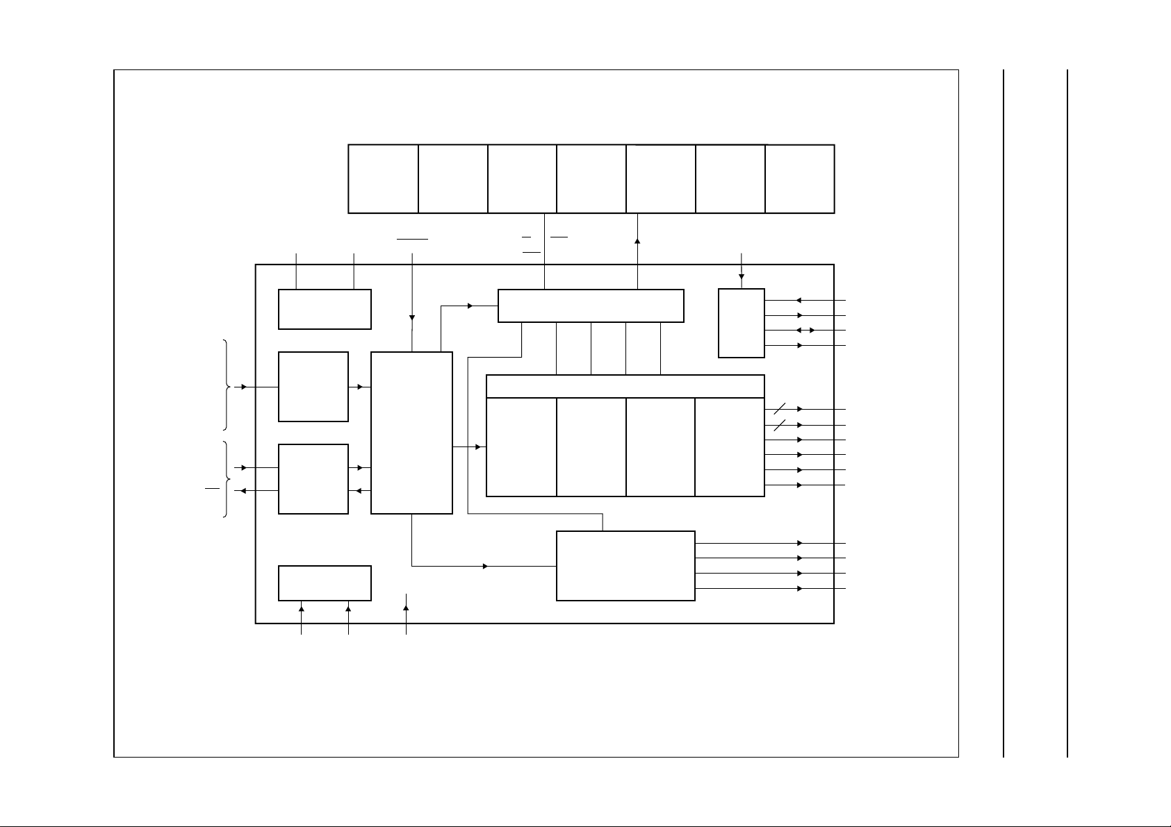
BLOCK DIAGRAM
Philips Semiconductors Preliminary specification
Video CD (VCD) decoder SAA2510
EBUIN
AUDIOCLK
WSIN
CLIN
EFIN
DAIN
NDAV
SDA
SCL
INT
ASEL
EXTERNAL
4 Mbit DRAM
Sys_osc_1 Sys_osc_0
76
SYSTEM CLOCK
BLOCK
DECODER
HOST
2
I
C
INTERFACE
BUFFER
74 27 79
SAA2510
TEST CONTROL
OSD
3 k 7 k
RESET CDIR
SYSTEM
CONTROLLER
PLAY
CONTROL
BUFFER
AUDIO
FIFO
W
RAS
MEMORY MANAGEMENT UNIT
DATA
SORTER
VIDEO
FIFO
CAS
A0 to A8 DR0 to DR15
VIDEO DECODER
IDCT
AUDIO DECODER
VIDEO
BUFFER
0
FRAME
RECON-
STRUCTOR
VIDEO
BUFFER
1
VIDEO
CLOCK
VIDEO
GENERATOR
VIDEO
BUFFER
2
8
95 to 88
8
7 to 1
100
84
86
82
80
99
97
11
9
12
13
16
14
Vid_osc_0
Vid_osc_1
CLK27
CREF
UV0 to UV7
Y0 to Y7
VSYNC
HREF
TLSAND
CSYNC
EBUOUT
DAOUT
CLOUT
WSOUT
77 78 28
TP1 TP2 DRAMON
MGE325
Fig.1 Block diagram.
Page 5

Philips Semiconductors Preliminary specification
Video CD (VCD) decoder SAA2510
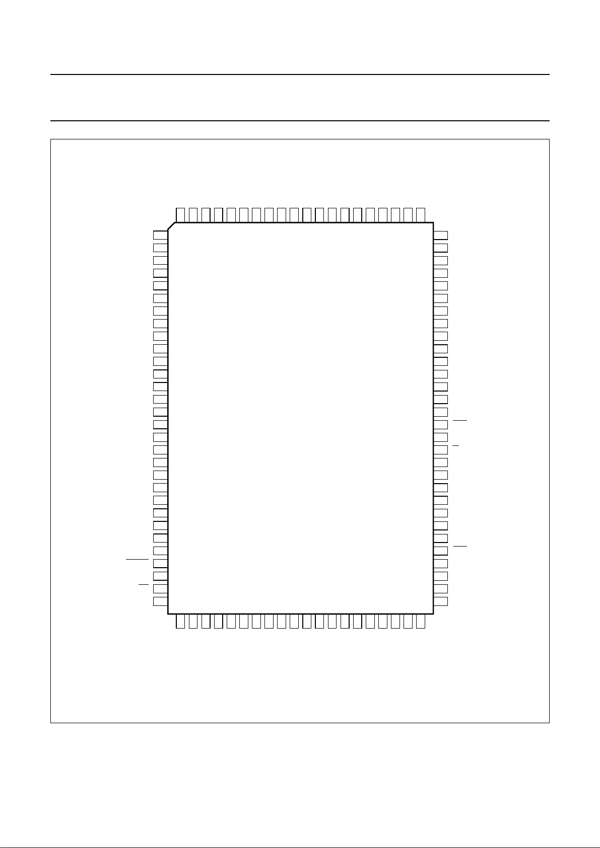
PINNING
SYMBOL PIN DESCRIPTION
UV6 1 video UV bus output bit 6;
16-bit video output mode: the UV bus outputs alternating U and V chroma samples
at 13.5 Mbytes/s
CCIR656 mode: this bus is not used (inactive)
UV5 2 video UV bus bit 5
UV4 3 video UV bus bit 4
UV3 4 video UV bus bit 3
UV2 5 video UV bus bit 2
UV1 6 video UV bus bit 1
UV0 7 video UV bus bit 0
V
DD5
CSYNC 9 composite sync output; 525 lines/60 Hz or 625 lines/50 Hz
V
SS5
TLSAND 11 two-level Sandcastle (composite blanking) output; requires external resistor network
EBUOUT 12 IEC 958 digital audio output
DAOUT 13 I
WSOUT 14 I
V
DD3
CLOUT 16 I
V
SS
AUDIOCLK 18 16.9 MHz audio clock input
V
DD5
EBUIN 20 EBU (IEC 958) input
CLIN 21 I
WSIN 22 I
DAIN 23 I
V
DD3
EFIN 25 error flag input from I
V
SS
RESET 27 active low reset input
DRAMON 28 DRAM pin 3-state control input; also 3-states video outputs and some timing signals
INT 29 active low open drain interrupt request to host microcontroller
NDAV 30 data not valid input (data on I
ASEL 31 I
SDA 32 I
V
DD5
SCL 34 I
V
SS5
DR15 36 DRAM data input/output bit 5
8 5 V external pad power supply
10 0 V external pad power supply
to define horizontal/vertical blanking level
2
S data; digital audio output
2
S word select digital audio output
15 +3 V internal power supply
2
S bit clock output
17 0 V internal power supply
19 5 V internal power supply
2
S bit clock input
2
S word select input
2
S digital data input
24 +3 V internal power supply
2
S source
26 0 V internal power supply
2
C-bus address select pin
2
C-bus data pin
33 5 V external pad power supply
2
C-bus clock input
35 0 V external pad power supply
2
S or EBU input not valid)
1996 May 21 5
Page 6

Philips Semiconductors Preliminary specification
Video CD (VCD) decoder SAA2510
SYMBOL PIN DESCRIPTION
DR14 37 DRAM data input/output bit 14
DR13 38 DRAM data input/output bit 13
DR12 39 DRAM data input/output bit 12
DR11 40 DRAM data input/output bit 11
DR10 41 DRAM data input/output bit 10
DR9 42 DRAM data input/output bit 9
V
DD5
DR8 44 DRAM data input/output bit 8
V
SS5
DR7 46 DRAM data input/output bit 7
DR6 47 DRAM data input/output bit 6
DR5 48 DRAM data input/output bit 5
DR4 49 DRAM data input/output bit 4
DR3 50 DRAM data input/output bit 3
DR2 51 DRAM data input/output bit 2
DR1 52 DRAM data input/output bit 1
DR0 53 DRAM data input/output bit 0
V
SS5
CAS 55 DRAM column address strobe
V
DD5
A8 57 DRAM row/column address pin A8
A7 58 DRAM row/column address pin A7
A6 59 DRAM row/column address pin A6
A5 60 DRAM row/column address pin A5
A4 61 DRAM row/column address pin A4
V
DD3
W 63 active low DRAM write strobe
V
SS
RAS 65 DRAM row address strobe
V
DD5
A3 67 DRAM row/column address pin A3
V
SS5
A2 69 DRAM row/column address pin A2
V
DD5
A1 71 DRAM row/column address pin A1
A0 72 DRAM row/column address pin A0
V
DDO3
Sys_osc_0 74 oscillator input pin; 40 MHz oscillator
V
SS
Sys_osc_1 76 oscillator output pin; 40 MHz oscillator
TP1 77 factory test pin; connect to ground
43 5 V external pad power supply
45 0 V external pad power supply
54 0 V external pad power supply
56 5 V external pad power supply
62 +3 V internal power supply
64 0 V internal power supply
66 5 V internal power supply
68 0 V external pad power supply
70 5 V external pad power supply
73 3 V internal power supply for oscillator
75 0 V internal power supply
1996 May 21 6
Page 7

Philips Semiconductors Preliminary specification
Video CD (VCD) decoder SAA2510
SYMBOL PIN DESCRIPTION
TP2 78 factory test pin; connect to ground
CDIR 79 clock direction control pin; when high, CLK27 is an output
CREF 80 clock qualifier output; 13.5 MHz timing signal used in 16-bit video output mode; can
also be used as 13.5 MHz video sample clock
V
SS5
CLK27 82 27 MHz clock input or output; direction controlled by CDIR pin
V
DD5
Vid_osc_0 84 oscillator pin; 27 MHz; input pin
V
SS
Vid_osc_1 86 oscillator pin; 27 MHz; output pin
V
DDO3
Y7 88 video Y bus output bit 7
Y6 89 video Y bus bit 6
Y5 90 video Y bus bit 5
Y4 91 video Y bus bit 4
Y3 92 video Y bus bit 3
Y2 93 video Y bus bit 2
Y1 94 video Y bus bit 1
Y0 95 video Y bus bit 0
V
SS5
HREF 97 horizontal (line) timing reference signal; high during active video part of line, low
V
DD5
VSYNC 99 vertical (field/frame) timing reference signal; high during vertical blanking interval of
UV7 100 video UV bus output bit 7
81 0 V external pad power supply
83 5 V external pad power supply
85 0 V internal power supply
87 3 V internal power supply for oscillator
DMSD mode: the Y bus outputs luminance samples at 13.5 Mbytes/s
CCIR656 mode: this pin supplies multiplexed chrominance and luminance
(27 Mbytes/s)
96 0 V external pad power supply
during line blanking
98 5 V external pad power supply
field
DMSD mode: the UV bus outputs alternating U and V chroma samples at
13.5 Mbytes/s
CCIR656 mode: this bus is not used (inactive)
1996 May 21 7
Page 8
Philips Semiconductors Preliminary specification
Video CD (VCD) decoder SAA2510
handbook, full pagewidth
DD5
UV6
UV5
UV4
UV3
UV2
UV1
UV0
V
DD5
CSYNC
V
SS5
TLSAND
EBUOUT
DAOUT
WSOUT
V
DD3
CLOUT
V
SS
AUDIOCLK
V
DD5
EBUIN
CLIN
WSIN
DAIN
V
DD3
EFIN
V
SS
RESET
DRAMON
INT
NDAV
UV7
VSYNC
99989796959493929190898887868584838281
100
1
2
3
4
5
6
7
8
9
10
11
12
13
14
15
16
17
18
19
20
21
22
23
24
25
26
27
28
29
30
SS5
V
HREF
V
Y0Y1Y2Y3Y4Y5Y6Y7V
SAA2510
DDO3
Vid_osc_1
DD5
VSSVid_osc_0
V
CLK27
V
SS5
80
79
78
77
76
75
74
73
72
71
70
69
68
67
66
65
64
63
62
61
60
59
58
57
56
55
54
53
52
51
CREF
CDIR
TP2
TP1
Sys_osc_1
V
SS
Sys_osc_0
V
DDO3
A0
A1
V
DD5
A2
V
SS5
A3
V
DD5
RAS
V
SS
W
V
DD3
A4
A5
A6
A7
A8
V
DD5
CAS
V
SS5
DR0
DR1
DR2
31323334353637383940414243444546474849
SS5
SCL
DD5
ASEL
SDA
V
DR15
DR14
DR13
V
DR12
Fig.2 Pin configuration.
1996 May 21 8
DR11
DR10
DR9VDD5
DR8
SS5
V
DR7
DR6
DR5
DR4
50
DR3
MGE324
Page 9

Philips Semiconductors Preliminary specification
Video CD (VCD) decoder SAA2510
FUNCTIONAL DESCRIPTION
Block decoder
The VCD chip receives MPEG A/V or CD digital audio data
from a CD decoder chipset using any one of four common
interface formats (Philips I
Philips I2S, EIAJ and Matsushita input modes use the bit
clock (CLIN), word select (WSIN), data (DAIN) and error
flag (EFIN) inputs. If IEC 958 (EBU) input mode is
selected, only the EBUIN pin needs to be connected. The
chip also requires a 16.9 MHz clock input (CLIN) which is
synchronous with the data input from the CD decoder
providing the serial data input.
The VCD chip contains a block decoder and descrambler
which performs error correction on the Video CD data track
(form 1) sectors and error detection on real-time audio and
video tracks where an error correction code is present.
In most events, audio output can be in any of the three
(I2S, EIAJ or MEC) formats, independent of input type.
When playing CD digital audio discs, the input is copied to
the outputs.
The block decoder supports some special functions which
enable recovery of play control lists. The desired sectors
can be acquired by programming a sector address via the
I2C-bus microcontroller interface. The microcontroller then
instructs the CD servo/decoder subsystem to execute a
servo jump to the required disc location and then waits for
an interrupt indicating that the desired sector information
has been received and error-corrected.
System controller
Overall control of the chip and a number of its less
time-critical functions is carried out by a dedicated
RISC processor. The microcode for this processor is
executed from an on-chip RAM. This microcode must be
loaded into RAM after power-up by the host
microcontroller, using the I
the functionality of the chip to be customized for specific
applications.
On-screen display
The VCD chip provides a bit-mapped On-Screen-Display
(OSD), containing 32 display lines of 352 pixels per line.
There is a double-height mode which repeats OSD lines so
that the maximum height of OSD objects becomes
64 lines. This character-set-independent OSD permits
display of ideographic characters and simple graphic
displays anywhere on the screen.
2
S, EIAJ, MEC or IEC 958). The
2
C-bus interface. This enables
The OSD is implemented as 48 vertical ‘slices’ of 8 pixels
(horizontally) and 32 (vertically). Each pixel is stored as
2 bits. This gives three programmable logical colours, plus
a transparent option. Each slice is identified by a slice code
(slice number).
The horizontal position of a slice is defined by its position
in a slice code sequence written to the VCD chip. This
arrangement reduces the need to completely update the
OSD bit map in many situations. It may be possible to
simply reorder the slices, e.g. if a track time display is
being updated and slices are prepared to represent digits.
At any time, up to 44 of the 48 slices can be displayed.
Video decoder
Video output data can be presented in one of two modes:
1. 16-bit wide data is output in YUV 4 : 2 : 2 format as
8 bits of luminance and 8 bits of alternating U and
V chrominance. The video output data rate in this
mode is 13.5 Mwords/s.
2. 8-bit wide, CCIR656-like, data is output providing
4:2:2 format video as an 8-bit UYVY multiplex at
27 Mbytes/s.
In either case, the VCD chip can be programmed to output
525 line or 625 line format timing to match the type of
display (TV) connected to its output. Additional
programmability is provided to cope with the Video CD disc
source picture coding type (525/625 lines).
The VCD chip performs vertical and horizontal
interpolation to convert the MPEG SIF (352 pixels per line)
normal resolution pictures to CCIR601 resolution.
Vertically interpolated pixels are output on the odd fields
during display of normal resolution pictures.
The Video CD disc being played may have been coded
with 525 lines/60 Hz or 625 lines/50 Hz pictures. When the
Video CD player is connected to a display with a different
timebase to the coded disc material, some adjustments
must be made to allow for the different number of lines on
the display and the reconstructed picture. Two examples
are shown in Figs. 3 and 4.
The VCD chip can be programmed to position the
reconstructed picture with respect to horizontal and
vertical syncs anywhere on the display screen with a
programmable ‘viewport’ position. Figure 3 shows an
MPEG SIF resolution picture (352 pixels by 288 lines)
being displayed on an NTSC display having only
240 active display lines per field. In this event, the top and
bottom 24 lines are not displayed.
1996 May 21 9
Page 10

Philips Semiconductors Preliminary specification
Video CD (VCD) decoder SAA2510
The second example, illustrated in Fig.4, is where a
240 active lines per field NTSC picture needs to be
displayed on a 288 line PAL format display. The ‘missing’
lines can be filled with a programmable border colour.
High-resolution still pictures can be present on a Video CD
disc.
24
24
reconstructed picture
352
not displayed
reconstructed picture
window
not displayed
240
MGE332
288
handbook, halfpage
Fig.3 One field of a 625-line picture on a 525-line
display.
In this event, the horizontal and vertical resolution of the
reconstructed picture is double that of normal resolution
(moving) pictures. In order to fit the picture in the available
frame buffer DRAM, a data compression scheme is
applied to the stored picture.
handbook, halfpage
display window
352
border = blank
viewport
border = blank
240
MGE333
288
Fig.4 525-line picture on a 625-line display.
1996 May 21 10
Page 11

Philips Semiconductors Preliminary specification
Video CD (VCD) decoder SAA2510
‘Trickmode’ implementation
Compared with CD digital audio players, it is likely that
Video CD players will need to offer additional functionality
similar to VCRs. These features are commonly called
‘trickmodes’. Typically, the player will offer features such
as still picture (freeze frame), scan forwards and
backwards as well as slow motion replay.
These features require a combination of CD servo control
and Video CD decoder functions for effective
implementation. The VCD chip provides high level
command features to support these modes in order to
minimize microcontroller time-critical software.
S
TILL PICTURE DISPLAY
This is implemented directly using a Pause command,
causing the VCD chip to hold the displayed picture at the
next frame update.
S
CAN FORWARD AND SCAN BACKWARDS
There is no difference as far as the VCD chip is concerned.
The controlling microcomputer must command the CD
servo to execute a servo jump and re-synchronize. The
VCD chip is then commanded to display the next I
(Intra-coded) picture following re-acquisition of sector
sync.
LOW-MOTION REPLAY
S
A command is provided by the VCD chip, allowing a
slow-motion ‘factor’ in the range 2 to 8 to be selected. This
is the factor by which replay will be slowed down. Because
the rate of decoding of video sectors has been reduced,
the video FIFO fills up. The block decoder is designed to
automatically disable acquisition when the video FIFO fills
in this way and an interrupt is generated. At this point, the
next wanted sector (address) has been loaded into a
register in the VCD chip. The controlling microcomputer
then commands a CD servo jump to position on the disc
just before the next desired sector, making allowance for
re-synchronization by the servo and VCD chip.
2
C-bus interface
I
The VCD chip is programmed via the I2C-bus interface.
The chip is a slave transceiver capable of operating at the
maximum specified bus clock frequency of 400 kHz. It
does not support the general call feature. One of two slave
addresses can be used. The address is selected by the
ASEL input pin.
to read data stored in three play-control sector buffers,
which normally will be used to store Video CD data track
information. This interface features a two or three byte
sub-addressing scheme allowing access to any DRAM
location. However, in normal use, only two byte
sub-addressing is needed.
An interrupt pin is available to signal a number of events
so that the controlling processor does not need to poll VCD
status registers.
Input pin NDAV is used to signal that data on the block
decoder input is not valid, e.g. during CD servo jumps.
A complete memory map and list of registers will be
included in a later version of this data sheet.
2
I
C-bus slave address selection
A6 A5 A4 A3 A2 A1 A0 R/W
001101A0
(1)
Note
1. ASEL.
The data transfer protocol is as follows:
Two and three byte sub-addressing: first the device
sub-address is transmitted, preceded by a START
condition and the slave address:
Two and three byte sub-addressing
S SLA W SUB_A
S = START
SLA = Slave address
W = Write
SUB_A = Sub-address
The sub-address can be either 2 or 3 bytes. The 3-byte
sub-address is used for DRAM random access. This is not
used for normal operation. It exists only as a test mode.
Since the Video CD IC is internally fully word (16 bits)
oriented, the sub-address must always be an even
address. If an odd-numbered address is given, the Video
CD IC will not acknowledge this byte. For the sub-address,
the least significant byte is sent first. The second
sub-address byte contains 2 control bits.
This bus provides access to the internal registers of the
device. The bus is also used to write OSD slice data and
1996 May 21 11
Page 12

Philips Semiconductors Preliminary specification
Video CD (VCD) decoder SAA2510
Sub-address byte format
MSB LSB MSB LSB
A7 A6 A5 A4 A3 A2 A1 A0 C1 C0 A13 A12 A11 A10 A9 A8
When A0 is a ‘1’, the address byte is not acknowledged
(odd address).
Explanation of control bits
C0 = 0; 2-byte sub-address.
C0 = 1; 3-byte sub-address. The next byte transmitted is
also an address byte:
3-byte sub-address - most significant byte format
MSB LSB
0 0 0 A18 A17 A16 A15 A14
C1 = 0; sub-address post increment enabled. After each
transfer of 2 bytes, the address is automatically
incremented by 2.
C1 = 1; sub-address post increment disabled.
The master will terminate a read action by NOT
acknowledging the last read byte followed by a STOP
condition.
Set 2-byte sub-address and write (M + 1) bytes
I2C-bus transaction summary
The following notation is used to describe bus
transactions:
S: START condition generated by bus master
P: STOP condition generated by bus master
A: Acknowledge bit generated by master or slave
according to transaction type and stage
N: Negative acknowledge; acknowledge bit is not set by
bus master during last byte of a read
SLA: 7-bit slave address generated by bus master
W: R/W bit after slave address is set to write
R: R/W bit after slave address is set to read
SUB_N: Sub-address byte N (N = 0, 1 or 2); least
significant address byte is SUB_0
D(M): A data byte transmitted by master or slave on the
bus; D(0) is the first byte sent; as all transfers must be
an even number of bytes, it follows that M must be odd.
S SLA W A SUB_0 A SUB_1 A D(0) A D(1) A to D(M) A P
Set 2-byte sub-address and read (M + 1) bytes
S SLA W A SUB_0 A SUB_1 A S SLA R D(0) A D(1) A to D(M) N P
Set 3-byte sub-address and write (M + 1) bytes
S SLA W A SUB_0 A SUB_1 A SUB_2 A D(0) A D(1) A to D(M) A P
Set 3-byte sub-address and read (M + 1) bytes
S SLA W A SUB_0 A SUB_1 A SUB_2 A S SLA R A D(0) A D(1) A to D(M) N P
This addressing mode is valid only if sub-address auto incrementing is disabled. It is intended for fast polling of a status
register.
1996 May 21 12
Page 13

Philips Semiconductors Preliminary specification
Video CD (VCD) decoder SAA2510
Byte-order within words
LSB MSB
Word B15 B14 B13 B12 B11 B10 B9 B8 B7 B6 B5 B4 B3 B2 B1 B0
2
C-bus B7 B6 B5 B4 B3 B2 B1 B0 B15 B14 B13 B12 B11 B10 B9 B8
I
For each transmitted word (read or written) the least significant byte is transmitted first.
CHARACTERISTICS
= −20 to +70 °C; V
T
amb
SYMBOL PARAMETER CONDITIONS MIN. TYP. MAX. UNIT
Supplies
V
DD5
I
DD5
V
DD3
I
DD3
I
DD(tot)
supply voltage (5 V) range 4.5 5 5.5 V
V
DD5
supply voltage (3 V) range 3 3.3 3.6 V
V
DD3
total supply current − tbf tbf mA
Digital inputs
= 4.5 to 5.5 V; V
DD5
= 3.0 to 3.6 V; unless otherwise specified.
DD3
supply current − tbf tbf mA
supply current − tbf tbf mA
A
LL INPUTS (EXCEPT RESET AND OSCILLATOR INPUTS)
V
IL
V
IH
I
LI
C
i
LOW level input voltage −0.3 −+0.8 V
HIGH level input voltage 2 − VDD+ 0.5 V
input leakage current Vi=0toV
input capacitance −−10 pF
RESET INPUT:(SCHMITT INPUT)
V
IL
V
IH
I
LI
V
hys
LOW level input voltage −0.3 +2V
HIGH level input voltage 3.5 VDD+ 0.5 V
input leakage current Vi= 0 to V
hysteresis voltage
(VIH− VIL)
Inputs/outputs
SDA
V
IL
V
IH
I
LI
C
i
C
L
V
OL
V
OL
AND SCL (I
2
C-BUS DATA AND CLOCK)
LOW level input voltage −0.5 −+1.5 V
HIGH level input voltage 3 − VDD+ 0.5 V
input leakage current Vi= 0 to V
input capacitance −−10 pF
load capacitance −−400 pF
LOW level output voltage (IOL= 3.0 mA) 0 − 0.4 V
LOW level output voltage (IOL= 6.0 mA) 0 − 0.6 V
CLK27
V
IL
V
IH
LOW level input voltage −0.3 −+0.8 V
HIGH level input voltage 2.4 − VDD+ 0.5 V
DD
DD
DD
−10 −+10 µA
−10 +10 µA
1 −− V
−10 −+10 µA
1996 May 21 13
Page 14

Philips Semiconductors Preliminary specification
Video CD (VCD) decoder SAA2510
SYMBOL PARAMETER CONDITIONS MIN. TYP. MAX. UNIT
I
LI
C
i
V
OL
V
OH
t
r
t
f
DR15 TO DR0 (DRAM DATA I/O)
V
IL
V
IH
I
LI
C
i
C
L
V
OL
V
OH
t
r
t
f
Outputs
input leakage current Vi= 0 to V
DD
−10 −+10 µA
input capacitance −−10 pF
LOW level output voltage (IOL= 1.6 mA) 0 − 0.4 V
HIGH level output voltage (IOH= −0.2 mA) 2.6 − V
DD
V
input rise time 0.6 to 2.6 V −−4ns
input fall time 0.6 to 2.6 V −−4ns
LOW level input voltage −0.3 −+0.8 V
HIGH level input voltage 2 − VDD+ 0.5 V
input leakage current Vi= 0 to V
DD
−10 −+10 µA
input capacitance −−10 pF
load capacitance −−30 pF
LOW level output voltage (IOL= 1.6 mA) 0 − 0.4 V
HIGH level output voltage (IOH= −0.2 mA) 2.4 − V
output rise time 0.6 to 2.6 V; load = C
output fall time 0.6 to 2.6 V; load = C
L
L
3 − 10 ns
3 − 10 ns
DD
V
RAS, CAS, W, A0 TO A8 (DRAM CONTROL AND ADDRESS LINES)
V
OL
V
OH
C
L
t
r
t
f
LOW level output voltage (IOL= 1.6 mA) 0 − 0.4 V
HIGH level output voltage (IOH= −0.2 mA) 2.4 − V
load capacitance − 30 pF
output rise time 0.6 to 2.2 V; load = C
output fall time 0.6 to 2.2 V; load = C
Y0 TO Y7 (VIDEO OUTPUT Y BUS)
V
OL
V
OH
C
L
t
r
t
f
LOW level output voltage (IOL= 1.6 mA) 0 − 0.4 V
HIGH level output voltage (IOH= −0.2 mA) 2.4 − V
load capacitance −−30 pF
output rise time 0.6 to 2.6 V; load = C
output fall time 0.6 to 2.6 V; load = C
UV0 TO UV7 (VIDEO OUTPUT UV BUS)
V
OL
V
OH
C
L
t
r
t
f
LOW level output voltage (IOL= 1.6 mA) 0 − 0.4 V
HIGH level output voltage (IOH= -0.2 mA) 2.4 − V
load capacitance −−30 pF
output rise time 0.6 to 2.2 V; load = C
output fall time 0.6 to 2.2 V; load = C
INT (OPEN DRAIN; INTERRUPT)
V
OL
C
L
t
r
LOW level output voltage (IOL= 1.6 mA) 0 − 0.4 V
load capacitance −−30 pF
output rise time 0.6 to 2.2 V; load = C
DD
L
L
L
L
L
L
L
3 − 10 ns
3 − 10 ns
DD
−−4ns
−−4ns
DD
−−10 ns
3 − 10 ns
−−10 ns
V
V
V
1996 May 21 14
Page 15

Philips Semiconductors Preliminary specification
Video CD (VCD) decoder SAA2510
SYMBOL PARAMETER CONDITIONS MIN. TYP. MAX. UNIT
t
f
EBUOUT (IEC 958 OUT)
V
OL
V
OH
C
L
t
r
t
r
ALL OTHER INPUTS
V
OL
V
OH
C
L
t
r
t
f
2
S input/output timing; (Fig.5)
I
output fall time 0.6 to 2.2 V; load = C
L
−−10 ns
LOW level output voltage (IOL= 10 mA) 0 − 1V
HIGH level output voltage (IOH= −10 mA) V
−1 − V
DD5
DD
V
load capacitance −−50 pF
output rise time 0.8 V to (V
load = C
output fall time 0.8 V to (V
load = C
− 0.8 V);
DD5
L
− 0.8 V);
DD5
L
−−10 ns
−−10 ns
LOW level output voltage (IOL= 1.6 mA) 0 − 0.4 V
HIGH level output voltage (IOH= −0.2 mA) 2.4 − V
DD
V
load capacitance −−50 pF
output rise time 0.6 to 2.6 V; load = C
output fall time 0.6 to 2.6 V; load = C
L
L
−−30 ns
−−30 ns
INPUT TIMING
f
clk
t
clkH
t
clkL
t
su
input clock frequency − 2.118 − MHz
input clock HIGH period 166 −− ns
input clock LOW period 166 −− ns
set-up time (DAIN, EFIN,
WSIN)
t
h1
hold time DAIN, EFIN,
WSIN)
OUTPUT TIMING
f
clk
t
clkH
t
h2
output clock frequency − 2.118 − MHz
output clock HIGH period 166 −− ns
hold time (DAOUT,
WSOUT)
t
d
output delay time (DAOUT ,
WSOUT)
2
C-bus input/output timing (Fig.6)
I
100 kHz CLOCK FREQUENCY
f
clk
t
LOW
t
HIGH
t
SU;DAT
t
HD;DAT
t
SU;STO
clock frequency 0 − 100 kHz
clock LOW period 4.7 −− µs
period 4 −− µs
data set-up time 250 −− ns
data hold time 0 −− ns
set-up time clock HIGH to
STOP
95 −− ns
0 −− ns
195 −− ns
−−147 ns
4.7 −− µs
1996 May 21 15
Page 16

Philips Semiconductors Preliminary specification
Video CD (VCD) decoder SAA2510
SYMBOL PARAMETER CONDITIONS MIN. TYP. MAX. UNIT
t
BUF
t
HD;STA
t
SU;STA
t
r
t
f
400 kHz CLOCK FREQUENCY
f
clk
t
LOW
t
HIGH
t
SU;DAT
t
HD;DAT
t
SU;STO
t
BUF
t
HD;STA
t
SU;STA
t
r
t
f
Video Output Timing (Figs. 7 and 8)
set-up time STOP to
4.7 −− µs
START
START hold time 4 −− µs
set-up time clock rising
4.7 −− µs
edge to START
rise time (SDA and SCL) V
fall time (SDA and SCL) V
ILmin
ILmin
to V
to V
IHmax
IHmax
50 − 1000 ns
50 − 300 ns
clock frequency 0 − 400 kHz
clock LOW period 1.3 −− µs
period 0.6 −− µs
data set-up time 100 −− ns
data hold time 0 −− ns
set-up time clock HIGH to
0.6 −− µs
STOP
set-up time STOP to
1.3 −− µs
START
START hold time 0.6 −− µs
set-up time clock rising
0.6 −− µs
edge to START
rise time (SDA and SCL) V
fall time (SDA and SCL) V
ILmin
ILmin
to V
to V
IHmax
IHmax
50 − 300 ns
50 − 300 ns
16-
BIT VIDEO OUTPUT MODE
t
su
set-up time (CREF, HREF,
UV and Y valid to CLK27)
t
h2
hold time (CLK27 to CREF ,
HREF, UV and Y invalid)
t
su
set-up time (UV and Y
valid to CREF rising edge)
t
h1
hold time (CREF rising
edge to UV and Y invalid)
8-BIT VIDEO OUTPUT MODE
t
su
set-up time (HREF and Y
valid to CLK27)
t
h2
hold time (CLK27 to HREF
and Y invalid)
DRAM Timing (Fig.9)
t
CYC
t
RP
t
CSH
t
RCD
cycle time 130 −− ns
RAS pre-charge time 50 −− ns
CAS hold time 70 −− ns
RAS to CAS delay time 20 −− ns
1996 May 21 16
10 −− ns
3 −− ns
6 −− ns
10 −− ns
7 −− ns
5 −− ns
Page 17

Philips Semiconductors Preliminary specification
Video CD (VCD) decoder SAA2510
SYMBOL PARAMETER CONDITIONS MIN. TYP. MAX. UNIT
t
CAS
t
PC
t
CP
t
RSH
t
CRP
t
ASR
t
RAH
t
ASC
t
CAH
t
RCS
t
RCH
t
RRH
t
WCS
t
WCH
t
DS
t
DH
t
CAC
t
RAC
Crystal oscillators
CAS pulse width LOW 20 −− ns
page mode cycle time 50 −− ns
CAS pre-charge time 10 −− ns
RAS hold time after CAS 20 −− ns
CAS to RAS pre-charge
15 −− ns
time
row address set-up time 0 −− ns
row address hold time 10 −− ns
column address set-up
0 −− ns
time
column address hold time 15 −− ns
read command set-up time 0 −− ns
read command hold time
0 −− ns
(CAS)
read command hold time
0 −− ns
(RAN)
write command set-up
0 −− ns
time
write command hold time 15 −− ns
data-in set-up time 0 −− ns
data-in hold time 15 −− ns
read access time (CAS) −−20 ns
read access time (RAS) −−70 ns
40 MHz
V
SYSTEM CLOCK OSCILLATOR
osc(p-p)
oscillation amplitude
− tbf − V
(peak-to-peak)
G
G
C
C
f
OSC
v
m
i
fb
small signal voltage gain − tbf −
mutual conductance tbf −− mA/V
input capacitance −−tbf pF
feedback capacitance − tbf − pF
oscillation frequency − 40 − MHz
∆f frequency tolerance −−− ppm
27 MHz
V
SYSTEM CLOCK OSCILLATOR
osc(p-p)
oscillation amplitude
− tbf − V
(peak-to-peak)
G
V
G
m
C
i
small signal voltage gain − tbf −
mutual conductance tbf −− mA/V
input capacitance −−tbf pF
1996 May 21 17
Page 18

Philips Semiconductors Preliminary specification
Video CD (VCD) decoder SAA2510
SYMBOL PARAMETER CONDITIONS MIN. TYP. MAX. UNIT
C
fb
f
osc
∆f frequency tolerance −−− ppm
feedback capacitance − tbf − pF
oscillation frequency − 27 − MHz
handbook, full pagewidth
I2S bit clock
CLKIN
or
CLKOUT
2
I
S data
and
word select outputs
DAOUT, WSOUT
I2S data,
word select
and
error flags inputs
DAIN, WSIN, EFIN
t
clkL
t
d
t
su
Fig.5 I2S input/output timing.
t
clkH
t
h
t
h
MGE327
handbook, full pagewidth
t
HIGH
SCL
t
SU; STA
t
HD; STA
SDA
t
BUF
Fig.6 I2C-bus timing.
1996 May 21 18
t
LOW
t
SU; DAT
t
r
t
f
t
HD; DAT
t
SU;STO
MGE328
Page 19

Philips Semiconductors Preliminary specification
Video CD (VCD) decoder SAA2510
handbook, full pagewidth
27 MHz clock
(CLK27)
t
t
su
CREF
t
su1
HREF
t
su2
U0 (Cb0)
pixel #0
CSYNC
(1)
Timing applies to CLK27 when programmed as an input or an output of the SAA2510.
(1) CSYNC (HIGH-to-LOW) to first sample and HREF (LOW-to-HIGH) = 264.5/244.5 CLK27 periods (625 lines/525 lines mode).
h1
t
h1
t
h2
V0 (Cr0)
Y0 Y1
V718
Y719
pixel #719
t
h2
MGE329
Fig.7 16-bit video output mode timing.
handbook, full pagewidth
27 MHz clock
(CLK27)
HREF
Y bus
output
t
su
t
h1
Cb Cr
Y
pixel #0
Fig.8 8-bit video CCIR656 output mode timing.
1996 May 21 19
Y719
pixel #719
t
h2
MGE330
Page 20

Philips Semiconductors Preliminary specification
Video CD (VCD) decoder SAA2510
handbook, full pagewidth
RAS
CAS
ADDRESS
W
DRAM
data out
W
t
RP
t
ASR
t
WCS
t
RAH
t
RCD
t
RCS
t
RAC
t
CSH
t
ASC
t
t
CAS
PC
t
CAH
t
CAC
t
CYC
t
RSH
t
CRP
t
CP
t
RRH
t
RCH
READ
CYCLE
t
WCH
t
DH
VCD
data to
DRAM
t
DS
Fig.9 DRAM timing.
1996 May 21 20
WRITE
CYCLE
MGE331
Page 21

Philips Semiconductors Preliminary specification
Video CD (VCD) decoder SAA2510
APPLICATION INFORMATION
handbook, full pagewidth
COMPACT DISC
MECHANISM
DECODER
MICROCONTROLLER
USER INTERFACE
AND
AND
2
I
C-bus
4 Mbit
DRAM
EBU input
16
9
40 MHz
crystal
Sys_osc_0 Sys_osc_1
EBUIN
AUDIOCLK
CLIN
DAIN
WSIN
ESIN
DR0 to DR15
A0 to A8
CASN
RASN
W
ASEL
SDA
SCL
RESET
NDAV
INTN
DRAMON
SAA2510
TEST1, 2
2
0 V
EBUOUT
CLOUT
DAOUT
WSOUT
HREF
VSYNC
UV0 to 7
Y0 to 7
CREF
CLK27
CDIR
Vid_osc_0
Vid_osc_1
0 V
EBU
INTERFACE
0 V
Audio L, R
CVBS
Y, C
2
C-bus
I
AUDIO DAC
DIGITAL
VIDEO
8
8
+5 V
ENCODER
VP0 to 7
CREF
LLC
e.g.: SAA7185
27 MHz
crystal
MGE326
VCD power supply pins not shown.
Fig.10 Application diagram; 16-bit video output mode.
1996 May 21 21
Page 22

Philips Semiconductors Preliminary specification
Video CD (VCD) decoder SAA2510
PACKAGE OUTLINE
QFP100: plastic quad flat package;
100 leads (lead length 1.95 mm); body 14 x 20 x 2.7 mm; high stand-off height
c
y
X
SOT317-1
80 51
81
pin 1 index
100
1
w M
b
0.25
p
0.40
0.25
D
H
D
D
0.25
20.1
0.13
19.9
e
DIMENSIONS (mm are the original dimensions)
mm
A
max.
3.3
0.36
0.10
2.87
2.57
UNIT A1A2A3bpcE
Z
D
0 5 10 mm
(1)
(1) (1)(1)
14.1
13.9
50
Z
E
e
w M
b
p
31
30
v M
B
v M
scale
eH
H
D
24.2
0.65
23.6
E
18.2
17.6
LL
A
A
H
E
E
A
B
p
1.0
0.6
2
A
A
1
detail X
Zywv θ
Z
D
0.151.95 0.10.2
0.8
0.4
E
1.0
0.6
(A )
3
θ
L
p
L
o
7
o
0
Note
1. Plastic or metal protrusions of 0.25 mm maximum per side are not included.
OUTLINE
VERSION
SOT317-1
IEC JEDEC EIAJ
REFERENCES
1996 May 21 22
EUROPEAN
PROJECTION
ISSUE DATE
95-02-04
97-08-01
Page 23

Philips Semiconductors Preliminary specification
Video CD (VCD) decoder SAA2510
SOLDERING
Introduction
There is no soldering method that is ideal for all IC
packages. Wave soldering is often preferred when
through-hole and surface mounted components are mixed
on one printed-circuit board. However, wave soldering is
not always suitable for surface mounted ICs, or for
printed-circuits with high population densities. In these
situations reflow soldering is often used.
This text gives a very brief insight to a complex technology.
A more in-depth account of soldering ICs can be found in
our
“IC Package Databook”
Reflow soldering
Reflow soldering techniques are suitable for all QFP
packages.
The choice of heating method may be influenced by larger
plastic QFP packages (44 leads, or more). If infrared or
vapour phase heating is used and the large packages are
not absolutely dry (less than 0.1% moisture content by
weight), vaporization of the small amount of moisture in
them can cause cracking of the plastic body. For more
information, refer to the Drypack chapter in our
Reference Handbook”
Reflow soldering requires solder paste (a suspension of
fine solder particles, flux and binding agent) to be applied
to the printed-circuit board by screen printing, stencilling or
pressure-syringe dispensing before package placement.
Several techniques exist for reflowing; for example,
thermal conduction by heated belt. Dwell times vary
between 50 and 300 seconds depending on heating
method. Typical reflow temperatures range from
215 to 250 °C.
Preheating is necessary to dry the paste and evaporate
the binding agent. Preheating duration: 45 minutes at
45 °C.
(order code 9398 652 90011).
“Quality
(order code 9397 750 00192).
Wave soldering
Wave soldering is not recommended for QFP packages.
This is because of the likelihood of solder bridging due to
closely-spaced leads and the possibility of incomplete
solder penetration in multi-lead devices.
If wave soldering cannot be avoided, the following
conditions must be observed:
• A double-wave (a turbulent wave with high upward
pressure followed by a smooth laminar wave)
soldering technique should be used.
• The footprint must be at an angle of 45° to the board
direction and must incorporate solder thieves
downstream and at the side corners.
Even with these conditions, do not consider wave
soldering the following packages: QFP52 (SOT379-1),
QFP100 (SOT317-1), QFP100 (SOT317-2),
QFP100 (SOT382-1) or QFP160 (SOT322-1).
During placement and before soldering, the package must
be fixed with a droplet of adhesive. The adhesive can be
applied by screen printing, pin transfer or syringe
dispensing. The package can be soldered after the
adhesive is cured.
Maximum permissible solder temperature is 260 °C, and
maximum duration of package immersion in solder is
10 seconds, if cooled to less than 150 °C within
6 seconds. Typical dwell time is 4 seconds at 250 °C.
A mildly-activated flux will eliminate the need for removal
of corrosive residues in most applications.
Repairing soldered joints
Fix the component by first soldering two diagonallyopposite end leads. Use only a low voltage soldering iron
(less than 24 V) applied to the flat part of the lead. Contact
time must be limited to 10 seconds at up to 300 °C. When
using a dedicated tool, all other leads can be soldered in
one operation within 2 to 5 seconds between
270 and 320 °C.
1996 May 21 23
Page 24

Philips Semiconductors Preliminary specification
Video CD (VCD) decoder SAA2510
DEFINITIONS
Data sheet status
Objective specification This data sheet contains target or goal specifications for product development.
Preliminary specification This data sheet contains preliminary data; supplementary data may be published later.
Product specification This data sheet contains final product specifications.
Limiting values
Limiting values given are in accordance with the Absolute Maximum Rating System (IEC 134). Stress above one or
more of the limiting values may cause permanent damage to the device. These are stress ratings only and operation
of the device at these or at any other conditions above those given in the Characteristics sections of the specification
is not implied. Exposure to limiting values for extended periods may affect device reliability.
Application information
Where application information is given, it is advisory and does not form part of the specification.
LIFE SUPPORT APPLICATIONS
These products are not designed for use in life support appliances, devices, or systems where malfunction of these
products can reasonably be expected to result in personal injury. Philips customers using or selling these products for
use in such applications do so at their own risk and agree to fully indemnify Philips for any damages resulting from such
improper use or sale.
2
PURCHASE OF PHILIPS I
C COMPONENTS
2
Purchase of Philips I
components in the I2C system provided the system conforms to the I2C specification defined by
Philips. This specification can be ordered using the code 9398 393 40011.
C components conveys a license under the Philips’ I2C patent to use the
1996 May 21 24
Page 25

Philips Semiconductors Preliminary specification
Video CD (VCD) decoder SAA2510
NOTES
1996 May 21 25
Page 26

Philips Semiconductors Preliminary specification
Video CD (VCD) decoder SAA2510
NOTES
1996 May 21 26
Page 27

Philips Semiconductors Preliminary specification
Video CD (VCD) decoder SAA2510
NOTES
1996 May 21 27
Page 28

Philips Semiconductors – a worldwide company
Argentina: see South America
Australia: 34 Waterloo Road, NORTH RYDE, NSW 2113,
Tel. (02) 805 4455, Fax. (02) 805 4466
Austria: Computerstr. 6, A-1101 WIEN, P.O. Box 213,
Tel. (01) 60 101-1256, Fax. (01) 60 101-1250
Belarus: Hotel Minsk Business Center, Bld. 3, r. 1211,
Volodarski Str. 6, 220050 MINSK,
Tel. (172) 200 733, Fax. (172) 200 773
Belgium: see The Netherlands
Brazil: see South America
Bulgaria: Philips Bulgaria Ltd., Energoproject, 15th floor,
51 James Bourchier Blvd., 1407 SOFIA,
Tel. (359) 2 689 211, Fax. (359) 2 689 102
Canada: PHILIPS SEMICONDUCTORS/COMPONENTS:
Tel. (800) 234-7381, Fax. (708) 296-8556
Chile: see South America
China/Hong Kong: 501 Hong Kong Industrial Technology Centre,
72 Tat Chee Avenue, Kowloon Tong, HONG KONG,
Tel. (852) 2319 7888, Fax. (852) 2319 7700
Colombia: see South America
Czech Republic: see Austria
Denmark: Prags Boulevard 80, PB 1919, DK-2300
COPENHAGEN S, Tel. (032) 88 2636, Fax. (031) 57 1949
Finland: Sinikalliontie 3, FIN-02630 ESPOO,
Tel. (358) 0-615 800, Fax. (358) 0-61580 920
France: 4 Rue du Port-aux-Vins, BP317,
92156 SURESNES Cedex,
Tel. (01) 4099 6161, Fax. (01) 4099 6427
Germany: P.O. Box 10 51 40, 20035 HAMBURG,
Tel. (040) 23 53 60, Fax. (040) 23 53 63 00
Greece: No. 15, 25th March Street, GR 17778 TAVROS,
Tel. (01) 4894 339/4894 911, Fax. (01) 4814 240
Hungary: see Austria
India: Philips INDIA Ltd, Shivsagar Estate, A Block,
Dr. Annie Besant Rd. Worli, BOMBAY 400 018
Tel. (022) 4938 541, Fax. (022) 4938 722
Indonesia: see Singapore
Ireland: Newstead, Clonskeagh, DUBLIN 14,
Tel. (01) 7640 000, Fax. (01) 7640 200
Israel: RAPAC Electronics, 7 Kehilat Saloniki St, TEL AVIV 61180,
Tel. (03) 645 04 44, Fax. (03) 648 10 07
Italy: PHILIPS SEMICONDUCTORS,
Piazza IV Novembre 3, 20124 MILANO,
Tel. (0039) 2 6752 2531, Fax. (0039) 2 6752 2557
Japan: Philips Bldg 13-37, Kohnan 2-chome, Minato-ku,
TOKYO 108, Tel. (03) 3740 5130, Fax. (03) 3740 5077
Korea: Philips House, 260-199 Itaewon-dong,
Yongsan-ku, SEOUL, Tel. (02) 709-1412, Fax. (02) 709-1415
Malaysia: No. 76 Jalan Universiti, 46200 PETALING JAYA,
SELANGOR, Tel. (03) 750 5214, Fax. (03) 757 4880
Mexico: 5900 Gateway East, Suite 200, EL PASO,
TEXAS 79905, Tel. 9-5(800) 234-7831, Fax. (708) 296-8556
Middle East: see Italy
Netherlands: Postbus 90050, 5600 PB EINDHOVEN, Bldg. VB,
Tel. (040) 2783749, Fax. (040) 2788399
New Zealand: 2 Wagener Place, C.P.O. Box 1041, AUCKLAND,
Tel. (09) 849-4160, Fax. (09) 849-7811
Norway: Box 1, Manglerud 0612, OSLO,
Tel. (022) 74 8000, Fax. (022) 74 8341
Philippines: PHILIPS SEMICONDUCTORS PHILIPPINES Inc.,
106 Valero St. Salcedo Village, P.O. Box 2108 MCC,
MAKATI, Metro MANILA,
Tel. (63) 2 816 6380, Fax. (63) 2 817 3474
Poland: Ul. Lukiska 10, PL 04-123 WARSZAWA,
Tel. (022) 612 2831, Fax. (022) 612 2327
Portugal: see Spain
Romania: see Italy
Singapore: Lorong 1, Toa Payoh, SINGAPORE 1231,
Tel. (65) 350 2000, Fax. (65) 251 6500
Slovakia: see Austria
Slovenia: see Italy
South Africa: S.A. PHILIPS Pty Ltd.,
195-215 Main Road Martindale, 2092 JOHANNESBURG,
P.O. Box 7430 Johannesburg 2000,
Tel. (011) 470-5911, Fax. (011) 470-5494
South America: Rua do Rocio 220 - 5th floor, Suite 51,
CEP: 04552-903-SÃO PAULO-SP, Brazil,
P.O. Box 7383 (01064-970),
Tel. (011) 821-2333, Fax. (011) 829-1849
Spain: Balmes 22, 08007 BARCELONA,
Tel. (03) 301 6312, Fax. (03) 301 4107
Sweden: Kottbygatan 7, Akalla. S-16485 STOCKHOLM,
Tel. (0) 8-632 2000, Fax. (0) 8-632 2745
Switzerland: Allmendstrasse 140, CH-8027 ZÜRICH,
Tel. (01) 488 2211, Fax. (01) 481 77 30
Taiwan: PHILIPS TAIWAN Ltd., 23-30F, 66,
Chung Hsiao West Road, Sec. 1, P.O. Box 22978,
TAIPEI 100, Tel. (886) 2 382 4443, Fax. (886) 2 382 4444
Thailand: PHILIPS ELECTRONICS (THAILAND) Ltd.,
209/2 Sanpavuth-Bangna Road Prakanong, BANGKOK 10260,
Tel. (66) 2 745-4090, Fax. (66) 2 398-0793
Turkey: Talatpasa Cad. No. 5, 80640 GÜLTEPE/ISTANBUL,
Tel. (0212) 279 2770, Fax. (0212) 282 6707
Ukraine: PHILIPS UKRAINE,
2A Akademika Koroleva str., Office 165, 252148 KIEV,
Tel.380-44-4760297, Fax. 380-44-4766991
United Kingdom: Philips Semiconductors LTD.,
276 Bath Road, Hayes, MIDDLESEX UB3 5BX,
Tel. (0181) 730-5000, Fax. (0181) 754-8421
United States: 811 East Arques Avenue, SUNNYVALE,
CA 94088-3409, Tel. (800) 234-7381, Fax. (708) 296-8556
Uruguay: see South America
Vietnam: see Singapore
Yugoslavia: PHILIPS, Trg N. Pasica 5/v, 11000 BEOGRAD,
Tel. (381) 11 825 344, Fax. (359) 211 635 777
Internet: http://www.semiconductors.philips.com/ps/
For all other countries apply to: Philips Semiconductors,
Marketing & Sales Communications, Building BE-p,
P.O. Box 218, 5600 MD EINDHOVEN, The Netherlands,
Fax. +31-40-2724825
SCDS48 © Philips Electronics N.V. 1996
All rights are reserved. Reproduction in whole or in part is prohibited without the
prior written consent of the copyright owner.
The information presented in this document does not form part of any quotation
or contract, is believed to be accurate and reliable and may be changed without
notice. No liability will be accepted by the publisher for any consequence of its
use. Publication thereof does not convey nor imply any license under patent- or
other industrial or intellectual property rights.
Printed in The Netherlands
537021/1200/01/pp28 Date of release: 1996 May 21
Document order number: 9397 750 00851
 Loading...