

Page 1

INTEGRATED CIRCUITS
DATA SH EET
SAA2503
MPEG2 audio decoder
Objective specification
File under Integrated Circuits, IC01
1997 Jul 02
Page 2

Philips Semiconductors Objective specification
MPEG2 audio decoder SAA2503
FEATURES
• Single-chip MPEG2 multichannel audio decoder
• Decodes MPEG high quality audio:
– MPEG1 layer 2 (44.1 kHz)
– MPEG2 multichannel layer 2 (48 kHz)
– Supports pause frames
• Outputs 2 channels
– Quasi surround down-mixing for Left and Right Dolby
surround channel (Lt and Rt)
– Stereo down-mixing for stereo reproduction
– Stereo signal selection
– Single channel down-mixing
• Karaoke modes
• Linear PCM modes:
– Down-sampling from 96 to 48 kHz
– Pass 48 kHz signals
• Bitstream input interface I2S-bus (IEC 1937 formatted)
• IEC 958 output interface (IEC 1937 formatted)
• IEC 958 output simultaneously available while decoding
MPEG2
• I2C-bus control
• Output flags for direct control
• Stand-alone operation possible (self-booting)
• No external DRAM or SRAM required
• On-chip PLL for internal clock generation
• 13.5 or 27 MHz master clock
• 100 pins plastic LQFP package
• 5 V power supply.
APPLICATIONS
This IC is mainly intended for use in Digital Versatile Disc
(DVD) players. However it may also be used in any
application that is able to accept an MPEG2 audio
bitstreams such as:
• Set top boxes
• Multimedia PCs
• Digital television
• Next generation audio equipment.
GENERAL DESCRIPTION
The SAA2503 incorporates all necessary functions, such
as MPEG2 multichannel audio decoding plus
down-mixing, MPEG1 layer 2 decoding, Linear PCM
(LPCM) processing all producing high quality audio.
Together with the serial audio interfaces and the IEC 958
transmitter this allows for the complete audio function of a
DVD player in a single chip.
ORDERING INFORMATION
TYPE
NUMBER
SAA2503HT LQFP100 plastic low profile quad flat package; 100 leads; body 14 x 14 x 1.4 mm SOT407-1
1997 Jul 02 2
NAME DESCRIPTION VERSION
PACKAGE
Page 3
Philips Semiconductors Objective specification
MPEG2 audio decoder SAA2503
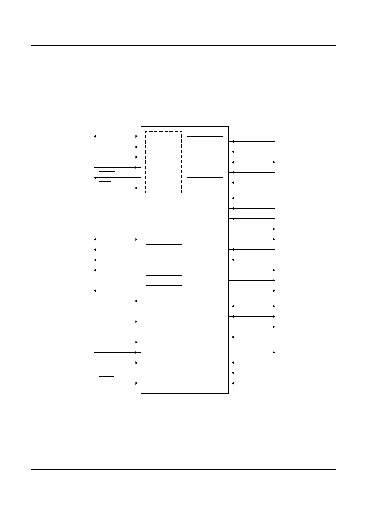
FUNCTIONAL I/O DIAGRAM
handbook, full pagewidth
H0 to H7
HA0 to HA2
HR/W
HEN
HOREQ
HACK/PB14
GPIO0 to GPIO3
I2CEN
BUSY
MUTE
ADO
ACI
resrved (19)
MODC
MODB
MODA
RESET
PARALLEL
HOST
INTERFACE
SAA2503
FLAGS
IEC 958
TRANSMITTER
reset
interrupt
I2C-BUS
SERIAL
HOST
INTERFACE
SERIAL
AUDIO
INTERFACE
OnCE
PLL
HA2
HA0
SDA
SLK
HREQ
SDB
SCKR
WSR
SCKT
WST
SDI0
SDI1
SDO0
SDO1
SDO2
DSCK/OS1
DSI/OS0
DSO
DR
PLOCK
PCAP
PINIT
EXTAL
Fig.1 Functional I/O diagram.
1997 Jul 02 3
MGK396
Page 4

Philips Semiconductors Objective specification
MPEG2 audio decoder SAA2503
PINNING
SYMBOL PIN I/O DESCRIPTION
n.c. 1 − not connected
n.c. 2 − not connected
GNDA1 3 GND ground 1 for some sections of internal logic
n.c. 4 − not connected
n.c. 5 − not connected
H7/PB7 6 I/O not used
H6/PB6 7 I/O not used
GNDH1 8 GND isolated ground 1 for the HI I/O drivers
HOA2/PB10 9 I/O not used
V
CCH1
HOA1/PB9 11 I/O not used
HR/
W/PB11 12 I/O not used
HEN/PB12 13 I/O not used
V
CCQ1
GNDQ1 15 GND isolated ground 1 for the internal logic
HACK/PB14 16 I/O not used
GNDH2 17 GND isolated ground 2 for the HI I/O drivers
HOA0/PB8 18 I/O not used
H5/PB5 19 I/O not used
V
CCH2
H4/PB4 21 I/O not used
H3/PB3 22 I/O not used
GNDH3 23 GND isolated ground 3 for the HI I/O drivers
H2/PB2 24 I/O not used
H1/PB1 25 I/O not used
H0/PB0 26 I/O not used
HOREQ/PB13 27 I/O not used
GNDH4 28 GND isolated ground 4 for the HI I/O drivers
V
CCH3
ADO 30 O digital audio data output
ACI 31 I audio clock input
n.c. 32 − not connected
n.c. 33 − not connected
n.c. 34 − not connected
PLOCK 35 O HIGH when PLL is phase locked
V
CCQ2
GNDQ2 37 GND isolated ground 2 for the internal logic
PINIT 38 I PLL enable/disable control
GNDP 39 GND ground dedicated for the PLL
PCAP 40 I PLL capacitor input
10 supply isolated power supply 1 for some sections of the internal chip logic
14 supply isolated power supply 1 for the HI I/O drivers
20 supply isolated power supply 2 for the HI I/O drivers
29 supply isolated power supply 3 for the HI I/O drivers
36 supply isolated power supply 2 for some sections of the internal chip logic
1997 Jul 02 4
Page 5

Philips Semiconductors Objective specification
MPEG2 audio decoder SAA2503
SYMBOL PIN I/O DESCRIPTION
V
CCP
EXTAL 42 I external clock/crystal Input
SCL 43 I I
GNDS1 44 GND isolated ground 1 for the SHI I/O drivers
SDA 45 I/O I
RESET 46 I hardware reset for the microcontroller
MODA 47 I mode select A
MODB 48 I mode select B
MODC 49 I mode select C
V
CCS1
HA0 51 I/O I
HA2 52 I I
HREQ 53 I host request
GNDS2 54 GND isolated ground 2 for the SHI I/O drivers
SDO2 55 O not used
SDO1 56 O not used
SDO0 57 O serial data output 0
V
CCS2
SCKT 59 O transmit serial clock
WST 60 O transmit word select
SCKR 61 I receive serial clock
GNDQ3 62 GND ground 3 dedicated for the PLL
V
CCQ3
GNDS3 64 GND isolated ground 3 for the SHI I/O drivers
WSR 65 I receive word select
SDI1 66 I serial data input 1
SDI0 67 I not used
DSO 68 O not used
DSI/OS0 69 O not used
DSCK/OS1 70 O not used
n.c. 71 − not connected
n.c. 72 − not connected
n.c. 73 − not connected
n.c. 74 − not connected
DR 75 I not used
SDB 76 I/O general purpose I/O
MUTE 77 I/O general purpose I/O
GNDD1 78 GND ground 1 for some sections of internal logic
BUSY 79 I/O general purpose I/O
I2CEN 80 I/O general purpose I/O
V
CCD1
41 supply supply voltage for the Phase Locked Loop (PLL)
2
C-bus serial clock
2
C-bus data and acknowledge
50 supply isolated power supply 1 for the SHI I/O drivers
2
C-bus slave address 0
2
C-bus slave address 2
58 supply isolated power supply 2 for the SHI I/O drivers
63 supply isolated power supply 3 for some sections of the internal chip logic
81 supply isolated power supply 1 for some sections of the internal chip logic
1997 Jul 02 5
Page 6

Philips Semiconductors Objective specification
MPEG2 audio decoder SAA2503
SYMBOL PIN I/O DESCRIPTION
GPIO3 82 I/O not used
GPIO2 83 I/O not used
GNDD2 84 GND ground 2 for some sections of internal logic
GPIO1 85 I/O not used
GPIO0 86 I/O not used
GNDQ4 87 GND ground 4 for some sections of internal logic
V
CCQ4
n.c. 89 − not connected
n.c. 90 − not connected
GNDA2 91 GND ground 2 for some sections of internal logic
n.c. 92 − not connected
V
CCA1
n.c. 94 − not connected
n.c. 95 − not connected
GNDA3 96 GND ground 3 for some sections of internal logic
n.c. 97 − not connected
n.c. 98 − not connected
n.c. 99 − not connected
V
CCA2
88 supply isolated power supply 4 for some sections of the internal chip logic
93 supply isolated power supply 1 for some sections of the internal chip logic
100 supply isolated power supply 2 for some sections of the internal chip logic
1997 Jul 02 6
Page 7

Philips Semiconductors Objective specification
MPEG2 audio decoder SAA2503
handbook, full pagewidth
n.c.
n.c.
GNDA1
n.c
n.c
H7/PB7
H6/PB6
GNDH1
HOA2/PB10
V
CCH1
HOA1/PB9
HR/W/PB11
HEN/PB12
V
CCQ1
GNDQ1
HACK/PB14
GNDH2
HOA0/PB8
H5/PB5
V
CCH2
H4/PB4
H3/PB3
GNDH3
H2/PB2
H1/PB1
CCA2
V
n.c
n.c
n.c
GNDA3
99989796959493929190898887868584838281
100
1
2
3
4
5
6
7
8
9
10
11
12
13
14
15
16
17
18
19
20
21
22
23
24
25
n.c
n.c
CCA1
V
n.c
GNDA2
n.c
CCQ4
n.c
V
SAA2503
GNDQ4
GPIO0
GPIO1
GNDD2
GPIO2
GPIO3
CCD1
BUSY
I2CEN
V
8079787776
GNDD1
MUTE
SDB
75
74
73
72
71
70
69
68
67
66
65
64
63
62
61
60
59
58
57
56
55
54
53
52
51
DR
n.c
n.c
n.c
n.c
DSCK/OS1
DSI/OS0
DSO
SDI0
SDI1
WSR
GNDS3
V
CCQ3
GNDQ3
SCKR
WST
SCKT
V
CCS2
SDO0
SDO1
SDO2
GNDS2
HREQ
HA2
HA0
26
H0/PB0
HOREQ/PB13
GNDH4
31323334353637383940414243444546474849
n.c
n.c
n.c.
ACI
ADO
CCH3
V
CCQ2
PLOCK
V
GNDQ2
30
29
28
27
Fig.2 Pin configuration.
1997 Jul 02 7
PINIT
GNDP
PCAP
V
CCP
SCL
EXTAL
SDA
GNDS1
MODA
RESET
MODB
MODC
50
CCS1
V
MGK395
Page 8

Philips Semiconductors Objective specification
MPEG2 audio decoder SAA2503
FUNCTIONAL DESCRIPTION
Operating modes
The SAA2503 can operate in 2 modes.
Stand-alone (mode 4)
In this mode (modC = 1, modB = 0 and modA = 0) the
SAA2503 boots itself from the internal program ROM after
power-up and can start decoding when a decoding mode
2
has been selected via the I
C-bus.
Booting via the I2C-bus (mode 7)
In this mode (modC = 1, modB = 1 and modA = 1) the
SAA2503 starts executing an internal boot program that
will receive 1536 bytes via the I2C-bus and then write
those to an on-chip program RAM.
This mode allows the standard behaviour (I/O interfaces,
additional processing) to be modified as specified in the
stand-alone mode.
Decoding modes
The SAA2503 has the following decoding modes:
• MPEG decoding (48 kHz DVD; 44.1 kHz VCD) IEC 958
LPCM
• MPEG decoding (48 kHz DVD; 44.1 kHz VCD) IEC 958
BITSTR
• LPCM CD-DA (44.1 kHz)
• LPCM down-sampling DVD (96 kHz: 4 channel input;
48 kHz 2 channel output)
• LPCM DVD (48 kHz: 8 channel input; 2 channel output).
System clock
The preferred system clock to be applied to the EXTAL pin
of the SAA2503 is 27 MHz if booted in mode 4
(stand-alone operation).
The internal PLL multiplies this clock by a factor of 3 to
obtain an 81 MHz internal clock.
If using another external clock frequency it is advisable to
ensure that:
• The internal PLL is disabled during booting when
f
> 27 MHz
clk(ext)
• That 10 MHz < (f
× 3) < 81 MHz.
clk(ext)
INTERFACING TO THE A/V SPLITTER
Serial audio interface
2
The serial audio interface can be configured as an I
S-bus
interface and when required, as Quad I2S interface.
The signal received via the I2S-bus is an encoded audio
bitstream in accordance with IEC 1937, or LPCM.
2
Table 1 Pinning of the I
S-bus interface
PINS DESCRIPTION PIN NUMBER DIRECTION
SDI0 high impedance 67 not used
SDI1 serial data 66 input/output
SDO0 serial data 57 output
SDO1 serial data 56 not used
SDO2 serial data 55 not used
SCKR I
2
S-bus clock; notes 1 and 2 61 input
WSR word select receive 65 input
SDB serial data begin 76 input
SCKT I
2
S-bus clock; notes 1 and 2 59 input
WST word select transmit 60 input
Notes
1. SCKT is equal to SCKR when the I2S-bus format is the format of the input signal. When Quad I2S-bus is used
SCKT =1⁄4SCKR.
2. The maximum allowed clock frequency for SCK is1⁄3f
(f
is the internal clock generated by the PLL of the
clk
clk
SAA2503).
1997 Jul 02 8
Page 9

Philips Semiconductors Objective specification
MPEG2 audio decoder SAA2503
MPEG2 bitstreams
The MPEG2 audio bitstream is received via the I2S-bus in
the same format as specified in IEC 1937. The MPEG2
audio bitstream consists of data bursts of 1 frame.
The data is formatted in 16-bit chunks. The time period
until the next frame is filled with logic 0. The serial data is
received by the SAA2503 via the SDI1 pin (pin 66).
For more information on transporting MPEG2 bitstreams
via IEC 958 see IEC 1937.
Linear PCM (LPCM)
2
S-BUS
I
Linear PCM samples are received in an I2S-bus format.
Serial audio data is received via SDI1 (pin 66).
The I2S-bus clock is received via SCKR (pin 61) and the
I2S-bus word select is received via WSR (pin 65); the
I2S-bus clock operates at 64fs.
handbook, full pagewidth
SD
Q0 Q1 Q2 Q3 Q4 Q5 Q6 Q7
QUAD I2S-BUS
Quad I2S-bus is the interface providing audio samples in
LPCM with 4 times the sampling frequency. The interface
is an extension of the I2S-bus where the Serial Data Begin
(SDB) indicates the first 2 channels out of 8 channels.
The audio samples are transferred with MSB first, where
each sample occupies 32 bits, filled with logic 0.
WS
SDB
SCK
12S-bus clock/Quad 12S-bus clock
1 sampling period
MGK398
Fig.3 Quad I2S-bus frame format.
The SDB remains HIGH when only 2 channels LPCM or encode bitstreams (in accordance with IEC 1937) are
transferred (Quad I
2
S-bus is equal to I2S-bus).
1997 Jul 02 9
Page 10

Philips Semiconductors Objective specification
MPEG2 audio decoder SAA2503
Table 2 Allocation of LPCM channels on Quad I2S-bus, fs=48or96kHz
NUMBER OF
LPCM CHANNELS
1 48 Q0 mute mute mute mute mute mute mute
2 48 Q0 Q1 mute mute mute mute mute mute
3 48 Q0 Q1 Q2 mute mute mute mute mute
4 48 Q0 Q1 Q2 Q3 mute mute mute mute
5 48 Q0 Q1 Q2 Q3 Q4 mute mute mute
6 48 Q0 Q1 Q2 Q3 Q4 Q5 mute mute
7 48 Q0 Q1 Q2 Q3 Q4 Q5 Q6 mute
8 48 Q0Q1Q2Q3Q4Q5Q6Q7
1 96 Q0 mute mute mute Q0 mute mute mute
2 96 Q0 Q1 mute mute Q0 Q1 mute mute
3 96 Q0 Q1 Q2 mute Q0 Q1 Q2 mute
4 96 Q0Q1Q2Q3Q0Q1Q2Q3
handbook, full pagewidth
SD
(kHz)
f
s
INPUT
CH0 CH1 CH2 CH3 CH4 CH5 CH6 CH7
channel n + 1
WS
SDB
SCK
channel n
0031
channel 0, 2, 4 or 6
31
channel 1, 3, 5 or 7
MGK397
Fig.4 Quad I2S-bus channel format.
1997 Jul 02 10
Page 11

Philips Semiconductors Objective specification
MPEG2 audio decoder SAA2503
AUDIO OUTPUTS INTERFACING
Also see Chapter “Interfacing to the A/V splitter”.
Stereo output for DAC
The output stereo down-mixing signal is in I
2
S-bus format
and can be directly connected to a DAC. The SDO0
(pin 57) provides the output for the serial audio data.
Furthermore, SCKT (pin 59) provides the I2S-bus clock
and WST (pin 60), the I2S-bus word select.
IEC 958 transmitter
The format of the IEC 958 interface consists of a sequence
of IEC 958 sub frames. Each IEC 958 sub frame is
normally used to carry one LPCM sample. The IEC 958
sub frame may also be used to convey data words.
The non-PCM encoded audio bitstreams to be transferred
are formed into data bursts. These bitstreams consist of a
sequence of data words.
Each data burst contains a 64-bit burst_preamble,
followed by the burst_payload.
Table 3 Pinning of IEC 958 interface
The burst_preamble provides a sync_word, information on
the burst_payload and the bitstream number.
The interface may convey one or more bitstreams. Each
type of bitstream may impose a particular requirement for
the repetition time for the data bursts that make up the
bitstream.
The 16-bit data words of a data burst are placed in time
slots 12 to 27 of an IEC 958 sub frame. In the consumer
application, both odd and even IEC 958-sub frames (CH1
and CH2) are simultaneously used to carry 32-bit data
words (32-bit mode). This allows the consumer IEC 958 to
convey either 2-channel LPCM audio, or a set of
alternating data words, but not both simultaneously.
For more information see IEC 1937.
The IEC 958 interface is of the digital audio interface. This
conveys LPCM or encoded audio bitstreams according to
IEC 1937 (IEC 1937), using the ‘network layer’ of IEC 958
(IEC 958). The audio data will be accompanied by a
validity bit, channel status and user data (sub code).
PINS DESCRIPTION PIN NUMBER DIRECTION
ADO Audio Data Output 30 output
ACI Audio Clock Input; note 1 31 input
Note
1. The ACI clock is 256f
INTERFACING WITH THE MICROCONTROLLER
Flags
The SAA2503 has 3 flags which, after a hardware reset,
are all initialized to logic 1.
2
C-bus communication disabled (pin 80); I2CEN: this
1. I
flag is set to logic 0 when the SAA2503 is ready to
accept messages via the I2C-bus.
2. Life test (pin 79); BUSY: when the SAA2503 operates
(or 512 or 384fs).
s
3. MPEG decoding active and synchronised (pin 77);
MUTE: when the SAA2503 operates in the MPEG
decoding mode, this flag indicates the state of the
SAA2503 (synchronized or not). When this pin is at
logic 1 the SAA2503 is out of sync, when set to logic 0
the SAA2503 is synchronized. It will not change state
when the SAA2503 remains synchronized. When the
SAA2503 is operating in one of the LPCM modes, the
MUTE pin is set at logic 1 during initialization and
logic 0 during processing.
in the MPEG decoding mode, this flag toggles
whenever the SAA2503 has detected a
synchronization pattern. The flag will then produce a
20.833 Hz (fas= 48 kHz) and a 19.140 Hz
(fas= 44.1 kHz) signal. It can be used to monitor the
MPEG decoding process. When this flag no longer
toggles there is an error. When the SAA2503 operates
in one of the LPCM modes however, the flag produces
either a 23.437 Hz (fas= 48 kHz) or a 21.533 Hz
(fas= 44.1 kHz) signal.
2
C-bus interface
I
The I2C-bus interface supports data rates of up to
400 kbits/s. For a description of the I2C-bus see
“The I2C-bus and how to use it”
, ordering number
9398 393 40011.
For a description of the I2C-bus commands controlling the
SAA2503 see Table 1.
1997 Jul 02 11
Page 12

Philips Semiconductors Objective specification
MPEG2 audio decoder SAA2503
APPLICATION SCHEMATIC
handbook, full pagewidth
RESET
POWER
GND
R134
10 kΩ
R135
10 kΩ
JP37
jumper
JP38
jumper
JP39
jumper
JP40
jumper
JP41
jumper
I2CEN
BUSY
MUTE
SDB
V
SS
26
H0/PB0
25
H1/PB1
24
H2/PB2
22
H3/PB3
21
H4/PB4
19
H5/PB5
7
H6/PB6
6
H7/PB7
18
HOA0/PB8
11
HOA1/PB9
9
HOA2/PB10
12
HR/W/PB11
13
HEN/PB12
27
HOREQ/PB13
16
HACK/PB14
86
GPIO0
85
GPIO1
83
GPIO2
82
GPIO3
80
I2CEN
79
BUSY
77
MUTE
76
SDB
L14
93 100 81 10 20 29 14 36 63 88 50 58
41
V
GNDP
39
CCP
CCA2
CCA1
CCD1
V
GNDD2
CCH1VCCH2VCCH3
V
HA0
HA2
SDA
V
V
GNDA1
GNDA2
GNDA3
3 91 96 78 84 8 17 23 28 15 37 62 87 44 451 52 45 43 53 47 48 49 46
GNDD1
CCQ1VCCQ2VCCQ3VCCQ4
V
SAA2503
SCL
HREQ
MODA
MODB
MODC
RESET
CCS1VCCS2
V
GNDH1
GNDH2
RESET
C73 C74 C75 C76
100 nF 100 nF 100 nF 100 nF
DSCK/OS1
DSI/OS0
GNDH3
GNDH4
GNDQ1
GNDQ2
GNDQ3
GNDQ4
GNDS1
n.c.
WSR
SCKR
SDI0
SDI1
WST
SCKT
SDO0
SDO1
SDO2
ADO
ACI
DSO
DR
PLOCK
PCAP
PINIT
EXTAL
GNDS2
54
65
61
67
66
60
59
57
56
55
30
31
70
69
68
75
35
40
38
42
WS-IN
SCK-IN
SD-IN
IEC 958
OUT (EBU)
A
B
C
D
E
F
G
H
I
J
jumper
JP42
jumper
MODE SETTINGS
2
I
C-BUS ADDRESS
SETTINGS
JP43
jumper
JP44
jumper
JP45
jumper
JP46
U11B
34
74HC04
MUTE
Fig.5 Application diagram (continued in Fig.6).
1997 Jul 02 12
R137
10 kΩ
R139
10 kΩ
R136
10 kΩ
R138
10 kΩ
R140
10 kΩ
SCL
SDA
JP
1
2
3
HEADER 3
2
I
C-BUS CONTROL
K
MGK399
Page 13

Philips Semiconductors Objective specification
MPEG2 audio decoder SAA2503
handbook, full pagewidth
serial audio data
from A/V splitter
A
B
C
D
E
F
G
H
I
J
BNC
JP50
jumper
HEADER 4
12
J2
1
74HC04
JP
U11A
R141
34
SDB
LED
2
D/A-CLK
16 14 15 7 8
n.c.
SSD
V
CLKS1
12
CLKS2
FILTCL
FILTCR
V
V
VOL
VOR
V
DDO
SSO
22
C
1 nF
23
25
C
1 nF
24
26
ref
C
100
nF
28
27
SYSCLK1
SYSCLK0
TDA1305
DDDVSSDVDDAVSSA
V
10
9
12
V
CC
D8
R142
470 Ω
C78
10
1.2 nF
kΩ
EMP1
EMP2
MUTE
SWS
SCK
DATA-L-R
V
CC
V
CC
5
WS
4
BCK
6
DATA
17
DEEM1
18
DEEM2
21
ATSB
19
MUSB
20
DSMB
13
n.c.
3
TEST1
11
TEST2
C
10 µF
C
10 µF
47 µF
R
47 kΩ
via OP-AMP to
analog output
47 kΩ
V
CC
100
C
nF
V
CC
DR
K
R143
4.7 kΩ
R110
100E
V
CC
74HC04 decoupling
C79
100 nF
5
OUT
GND
4
V
CC
BLM21A10
8
L7
U54
27 MHz OSC
V
CC
Fig.6 Application diagram (continued from Fig.5).
1997 Jul 02 13
C32
100 nF
C
100 nF
C
100 nF
C
47 µF
MGK400
Page 14

Philips Semiconductors Objective specification
MPEG2 audio decoder SAA2503
PACKAGE OUTLINE
LQFP100: plastic low profile quad flat package; 100 leads; body 14 x 14 x 1.4 mm
c
y
100
X
75
76
pin 1 index
1
e
w M
b
p
D
H
D
51
50
Z
E
26
25
Z
D
b
B
e
w M
p
v M
v M
A
H
E
E
A
B
A
2
A
A
1
detail X
SOT407-1
Q
(A )
3
θ
L
p
L
0 5 10 mm
scale
DIMENSIONS (mm are the original dimensions)
mm
OUTLINE
VERSION
SOT407-1
A
A1A2A3bpcE
max.
0.20
1.6
0.05
1.5
1.3
0.28
0.16
0.18
0.12
0.25
IEC JEDEC EIAJ
UNIT
Note
1. Plastic or metal protrusions of 0.25 mm maximum per side are not included.
(1)
(1) (1)(1)
D
14.1
13.9
REFERENCES
eH
14.1
13.9
0.5
16.25
15.75
1997 Jul 02 14
H
D
LLpQZywv θ
E
16.25
15.75
0.75
0.45
0.70
0.57
0.12 0.10.21.0
EUROPEAN
PROJECTION
Z
D
1.15
1.15
0.85
0.85
ISSUE DATE
95-12-19
E
o
7
o
0
Page 15

Philips Semiconductors Objective specification
MPEG2 audio decoder SAA2503
SOLDERING
Introduction
There is no soldering method that is ideal for all IC
packages. Wave soldering is often preferred when
through-hole and surface mounted components are mixed
on one printed-circuit board. However, wave soldering is
not always suitable for surface mounted ICs, or for
printed-circuits with high population densities. In these
situations reflow soldering is often used.
This text gives a very brief insight to a complex technology.
A more in-depth account of soldering ICs can be found in
“IC Package Databook”
our
Reflow soldering
Reflow soldering techniques are suitable for all LQFP
packages.
Reflow soldering requires solder paste (a suspension of
fine solder particles, flux and binding agent) to be applied
to the printed-circuit board by screen printing, stencilling or
pressure-syringe dispensing before package placement.
Several techniques exist for reflowing; for example,
thermal conduction by heated belt. Dwell times vary
between 50 and 300 seconds depending on heating
method. Typical reflow temperatures range from
215 to 250 °C.
Preheating is necessary to dry the paste and evaporate
the binding agent. Preheating duration: 45 minutes at
45 °C.
Wave soldering
Wave soldering is not recommended for LQFP packages.
This is because of the likelihood of solder bridging due to
closely-spaced leads and the possibility of incomplete
solder penetration in multi-lead devices.
(order code 9398 652 90011).
If wave soldering cannot be avoided, the following
conditions must be observed:
• A double-wave (a turbulent wave with high upward
pressure followed by a smooth laminar wave)
soldering technique should be used.
• The footprint must be at an angle of 45° to the board
direction and must incorporate solder thieves
downstream and at the side corners.
Even with these conditions, do not consider wave
soldering LQFP packages LQFP48 (SOT313-2),
LQFP64 (SOT314-2) or LQFP80 (SOT315-1).
During placement and before soldering, the package must
be fixed with a droplet of adhesive. The adhesive can be
applied by screen printing, pin transfer or syringe
dispensing. The package can be soldered after the
adhesive is cured.
Maximum permissible solder temperature is 260 °C, and
maximum duration of package immersion in solder is
10 seconds, if cooled to less than 150 °C within
6 seconds. Typical dwell time is 4 seconds at 250 °C.
A mildly-activated flux will eliminate the need for removal
of corrosive residues in most applications.
Repairing soldered joints
Fix the component by first soldering two diagonallyopposite end leads. Use only a low voltage soldering iron
(less than 24 V) applied to the flat part of the lead. Contact
time must be limited to 10 seconds at up to 300 °C. When
using a dedicated tool, all other leads can be soldered in
one operation within 2 to 5 seconds between
270 and 320 °C.
1997 Jul 02 15
Page 16

Philips Semiconductors Objective specification
MPEG2 audio decoder SAA2503
DEFINITIONS
Data sheet status
Objective specification This data sheet contains target or goal specifications for product development.
Preliminary specification This data sheet contains preliminary data; supplementary data may be published later.
Product specification This data sheet contains final product specifications.
Limiting values
Limiting values given are in accordance with the Absolute Maximum Rating System (IEC 134). Stress above one or
more of the limiting values may cause permanent damage to the device. These are stress ratings only and operation
of the device at these or at any other conditions above those given in the Characteristics sections of the specification
is not implied. Exposure to limiting values for extended periods may affect device reliability.
Application information
Where application information is given, it is advisory and does not form part of the specification.
LIFE SUPPORT APPLICATIONS
These products are not designed for use in life support appliances, devices, or systems where malfunction of these
products can reasonably be expected to result in personal injury. Philips customers using or selling these products for
use in such applications do so at their own risk and agree to fully indemnify Philips for any damages resulting from such
improper use or sale.
2
PURCHASE OF PHILIPS I
C COMPONENTS
2
Purchase of Philips I
components in the I2C system provided the system conforms to the I2C specification defined by
Philips. This specification can be ordered using the code 9398 393 40011.
C components conveys a license under the Philips’ I2C patent to use the
1997 Jul 02 16
Page 17

Philips Semiconductors Objective specification
MPEG2 audio decoder SAA2503
NOTES
1997 Jul 02 17
Page 18

Philips Semiconductors Objective specification
MPEG2 audio decoder SAA2503
NOTES
1997 Jul 02 18
Page 19

Philips Semiconductors Objective specification
MPEG2 audio decoder SAA2503
NOTES
1997 Jul 02 19
Page 20

Philips Semiconductors – a worldwide company
Argentina: see South America
Australia: 34 Waterloo Road, NORTH RYDE, NSW 2113,
Tel. +61 2 9805 4455, Fax. +61 2 9805 4466
Austria: Computerstr. 6, A-1101 WIEN, P.O. Box 213,
Tel. +43 1 60 101, Fax. +43 1 60 101 1210
Belarus: Hotel Minsk Business Center, Bld. 3, r. 1211, Volodarski Str. 6,
220050 MINSK, Tel. +375 172 200 733, Fax. +375 172 200 773
Belgium: see The Netherlands
Brazil: see South America
Bulgaria: Philips Bulgaria Ltd., Energoproject, 15th floor,
51 James Bourchier Blvd., 1407 SOFIA,
Tel. +359 2 689 211, Fax. +359 2 689 102
Canada: PHILIPS SEMICONDUCTORS/COMPONENTS,
Tel. +1 800 234 7381
China/Hong Kong: 501 Hong Kong Industrial Technology Centre,
72 Tat Chee Avenue, Kowloon Tong, HONG KONG,
Tel. +852 2319 7888, Fax. +852 2319 7700
Colombia: see South America
Czech Republic: see Austria
Denmark: Prags Boulevard 80, PB 1919, DK-2300 COPENHAGEN S,
Tel. +45 32 88 2636, Fax. +45 31 57 0044
Finland: Sinikalliontie 3, FIN-02630 ESPOO,
Tel. +358 9 615800, Fax. +358 9 61580920
France: 4 Rue du Port-aux-Vins, BP317, 92156 SURESNES Cedex,
Tel. +33 1 40 99 6161, Fax. +33 1 40 99 6427
Germany: Hammerbrookstraße 69, D-20097 HAMBURG,
Tel. +49 40 23 53 60, Fax. +49 40 23 536 300
Greece: No. 15, 25th March Street, GR 17778 TAVROS/ATHENS,
Tel. +30 1 4894 339/239, Fax. +30 1 4814 240
Hungary: see Austria
India: Philips INDIA Ltd, Shivsagar Estate, A Block, Dr. Annie Besant Rd.
Worli, MUMBAI 400 018, Tel. +91 22 4938 541, Fax. +91 22 4938 722
Indonesia: see Singapore
Ireland: Newstead, Clonskeagh, DUBLIN 14,
Tel. +353 1 7640 000, Fax. +353 1 7640 200
Israel: RAPAC Electronics, 7 Kehilat Saloniki St, PO Box 18053,
TEL AVIV 61180, Tel. +972 3 645 0444, Fax. +972 3 649 1007
Italy: PHILIPS SEMICONDUCTORS, Piazza IV Novembre 3,
20124 MILANO, Tel. +39 2 6752 2531, Fax. +39 2 6752 2557
Japan: Philips Bldg 13-37, Kohnan 2-chome, Minato-ku, TOKYO 108,
Tel. +81 3 3740 5130, Fax. +81 3 3740 5077
Korea: Philips House, 260-199 Itaewon-dong, Yongsan-ku, SEOUL,
Tel. +82 2 709 1412, Fax. +82 2 709 1415
Malaysia: No. 76 Jalan Universiti, 46200 PETALING JAYA, SELANGOR,
Tel. +60 3 750 5214, Fax. +60 3 757 4880
Mexico: 5900 Gateway East, Suite 200, EL PASO, TEXAS 79905,
Tel. +9-5 800 234 7381
Middle East: see Italy
Netherlands: Postbus 90050, 5600 PB EINDHOVEN, Bldg. VB,
Tel. +31 40 27 82785, Fax. +31 40 27 88399
New Zealand: 2 Wagener Place, C.P.O. Box 1041, AUCKLAND,
Tel. +64 9 849 4160, Fax. +64 9 849 7811
Norway: Box 1, Manglerud 0612, OSLO,
Tel. +47 22 74 8000, Fax. +47 22 74 8341
Philippines: Philips Semiconductors Philippines Inc.,
106 Valero St. Salcedo Village, P.O. Box 2108 MCC, MAKATI,
Metro MANILA, Tel. +63 2 816 6380, Fax. +63 2 817 3474
Poland: Ul. Lukiska 10, PL 04-123 WARSZAWA,
Tel. +48 22 612 2831, Fax. +48 22 612 2327
Portugal: see Spain
Romania: see Italy
Russia: Philips Russia, Ul. Usatcheva 35A, 119048 MOSCOW,
Tel. +7 095 755 6918, Fax. +7 095 755 6919
Singapore: Lorong 1, Toa Payoh, SINGAPORE 1231,
Tel. +65 350 2538, Fax. +65 251 6500
Slovakia: see Austria
Slovenia: see Italy
South Africa: S.A. PHILIPS Pty Ltd., 195-215 Main Road Martindale,
2092 JOHANNESBURG, P.O. Box 7430 Johannesburg 2000,
Tel. +27 11 470 5911, Fax. +27 11 470 5494
South America: Rua do Rocio 220, 5th floor, Suite 51,
04552-903 São Paulo, SÃO PAULO - SP, Brazil,
Tel. +55 11 821 2333, Fax. +55 11 829 1849
Spain: Balmes 22, 08007 BARCELONA,
Tel. +34 3 301 6312, Fax. +34 3 301 4107
Sweden: Kottbygatan 7, Akalla, S-16485 STOCKHOLM,
Tel. +46 8 632 2000, Fax. +46 8 632 2745
Switzerland: Allmendstrasse 140, CH-8027 ZÜRICH,
Tel. +41 1 488 2686, Fax. +41 1 481 7730
Taiwan: Philips Semiconductors, 6F, No. 96, Chien Kuo N. Rd., Sec. 1,
TAIPEI, Taiwan Tel. +886 2 2134 2865, Fax. +886 2 2134 2874
Thailand: PHILIPS ELECTRONICS (THAILAND) Ltd.,
209/2 Sanpavuth-Bangna Road Prakanong, BANGKOK 10260,
Tel. +66 2 745 4090, Fax. +66 2 398 0793
Turkey: Talatpasa Cad. No. 5, 80640 GÜLTEPE/ISTANBUL,
Tel. +90 212 279 2770, Fax. +90 212 282 6707
Ukraine: PHILIPS UKRAINE, 4 Patrice Lumumba str., Building B, Floor 7,
252042 KIEV, Tel. +380 44 264 2776, Fax. +380 44 268 0461
United Kingdom: Philips Semiconductors Ltd., 276 Bath Road, Hayes,
MIDDLESEX UB3 5BX, Tel. +44 181 730 5000, Fax. +44 181 754 8421
United States: 811 East Arques Avenue, SUNNYVALE, CA 94088-3409,
Tel. +1 800 234 7381
Uruguay: see South America
Vietnam: see Singapore
Yugoslavia: PHILIPS, Trg N. Pasica 5/v, 11000 BEOGRAD,
Tel. +381 11 625 344, Fax.+381 11 635 777
For all other countries apply to: Philips Semiconductors, Marketing & Sales Communications,
Building BE-p, P.O. Box 218, 5600 MD EINDHOVEN, The Netherlands, Fax. +31 40 27 24825
© Philips Electronics N.V. 1997 SCA54
All rights are reserved. Reproduction in whole or in part is prohibited without the prior written consent of the copyright owner.
The information presented in this document does not form part of any quotation or contract, is believed to be accurate and reliable and may be changed
without notice. No liability will be accepted by the publisher for any consequence of its use. Publication thereof does not convey nor imply any license
under patent- or other industrial or intellectual property rights.
Internet: http://www.semiconductors.philips.com
Printed in The Netherlands 547027/1200/01/pp20 Date of release: 1997 Jul 02 Document order number: 9397 750 01802
 Loading...