

Page 1

INTEGRATED CIRCUITS
DATA SH EET
SAA2500
MPEG Audio Source Decoder
Preliminary specification
File under Integrated Circuits, IC01
Philips Semiconductors
September 1994
Page 2

Philips Semiconductors Preliminary specification
MPEG Audio Source Decoder SAA2500
FEATURES
• Advanced error protection
• Integrated audio post processing for control of signal
level and inter-channel crosstalk
• Demultiplexing of ancillary data in the input bitstream
• Automatic digital de-emphasis of the decoded
audio signal
• Separate master and slave inputs
• Automatic sample frequency and bit-rate switching in
master input mode
• Automatic synchronization of input and output interface
clocks in master input mode
• Selectable audio output precision; 16, 18, 20 or 22 bit
• Low power consumption.
ORDERING INFORMATION
TYPE NUMBER
SAA2500H QFP44
NAME DESCRIPTION VERSION
(1)
Plastic quad flat package; 44 leads (lead length 1.3 mm);
body 10 × 10 × 1.75 mm
APPLICATIONS
• Cable and satellite digital radio decoders
• Video CD
• Compact Disc Interactive (CD-I)
• Sold-state audio
• Multimedia Personal Computer (PC).
GENERAL DESCRIPTION
The SAA2500 supports all audio modes (joint stereo,
stereo, single channel and dual channel) bit rates and
sample frequencies of ISO/MPEG-1 layers I and II, as
standardized in
PACKAGE
“ISO/IEC 11172-3”
.
SOT307-2
Note
1. When using IR reflow soldering it is recommended that the Drypack instructions in the
Pocketbook”
Supply of this
right under any patent, or any Industrial or Intellectual Property Right, to use this IC in any ready-to-use
electronic product.
(order number 9398 510 34011) are followed.
“ISO/IEC 11172-3”
audio standard Layer I or layer II compatible IC does not convey a licence nor imply a
“Quality Reference
September 1994 2
Page 3

Philips Semiconductors Preliminary specification
MPEG Audio Source Decoder SAA2500
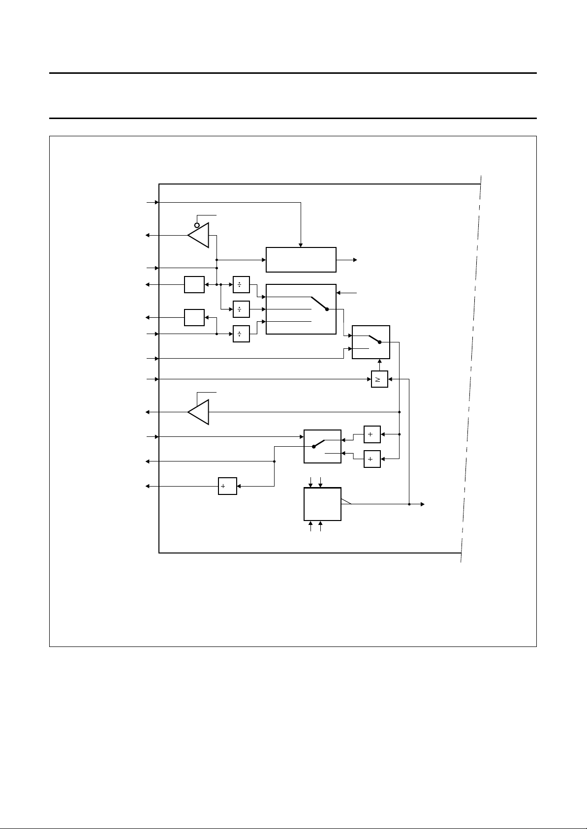
BLOCK DIAGRAM
handbook, full pagewidth
CDSEF
CDSCL
CDSWA
CDSSY
CDMEF
CDMCL
CDMWS
TDI
TDO
TCK
TMS
TRST
CDS
CDM
DD1
V
534
41
37
39
40
38
19
20
18
21
22
15
14
16
13
DD2
V
PROCESSOR
TC0 TC1
MCLK
MCLKIN
MCLKOUT
7444 10 9 3242 43 24 25 23 11 12
8
X22IN
MCLK24
CLOCK
GENERATOR
X22OUT
FSCLK
FSCLKIN
FSCLKM
FSCLK384
L3DATA
L3MODE
DECODING
CONTROL
L3CLK
SAA2500
SYNTHESYS
SUBBAND
FILTER
BANK
AND
OUTPUT
PROCESSING
INPUT
36 35
PROCESSOR
17
GND
DEQUANTI-
ZATION
AND
SCALING
GND
6
GND
TA TB TO TI SCK WS
URDA
STOP
1
RESET
26
SD
29 303231332728
MGB489
Fig.1 Functional block diagram.
September 1994 3
Page 4

Philips Semiconductors Preliminary specification
MPEG Audio Source Decoder SAA2500
PINNING
SYMBOL PIN DESCRIPTION TYPE
RESET 1 master reset I
FSCLK 2 sample rate clock; buffered signal O
FSCLKIN 3 sample rate clock input I
MCLK 4 master clock; buffered signal O
V
DD1
GND 6 supply ground −
MCLKOUT 7 master clock oscillator output O
MCLKIN 8 master clock oscillator input or signal input I
X22OUT 9 22.579 MHz clock oscillator output O
X22IN 10 22.579 MHz clock oscillator input or signal input I
STOP 11 stop decoding I
URDA 12 unreliable data input; interrupt decoding I
CDMWS 13 coded data (master input) word select output O
CDMEF 14 coded data (master input) error flag input I
CDM 15 ISO/MPEG coded data (master input) I
CDMCL 16 coded data (master input) bit clock output O
GND 17 supply ground −
CDSCL 18 coded data (slave input) bit clock I
CDS 19 ISO/MPEG coded data (slave input) I
CDSEF 20 coded data (slave input) error flag I
CDSWA 21 coded data (slave input) window signal I
CDSSY 22 coded data (slave input) frame sync I
L3CLK 23 L3 interface bit clock I
L3DATA 24 L3 interface serial data I/O
L3MODE 25 L3 interface address/data select input I
SD 26 baseband audio I
TA 27 do not connect; reserved O
GND 28 supply ground −
SCK 29 baseband audio data I
WS 30 baseband audio data I
TO 31 connect to TI (pin 32) O
TI 32 connect to TO (pin 31) I
TB 33 do not connect; reserved O
V
DD2
TC1 35 do not connect; factory test control 1 input, with integrated pull-down resistor I
TC0 36 do not connect; factory test control 0 input, with integrated pull-down resistor I
TDO 37 boundary scan test data output O
TRST 38 boundary scan test reset input; this pin should be connected to ground for
TCK 39 boundary scan test clock input I
5 supply voltage −
2
S data output O
2
S clock output O
2
S word select output O
34 supply voltage −
normal operation
I
September 1994 4
Page 5

Philips Semiconductors Preliminary specification
MPEG Audio Source Decoder SAA2500
SYMBOL PIN DESCRIPTION TYPE
TMS 40 boundary scan test mode select input I
TDI 41 boundary scan test data input I
FSCLK384 42 sample rate clock frequency indication input I
FSCLKM 43 sample rate clock source selection for the master input I
MCLK24 44 master clock frequency indication I
handbook, full pagewidth
handbook, full pagewidth
RESET
FSCLK
FSCLKIN
MCLK
V
DD
GND
MCLKOUT
MCLKIN
X22OUT
X22IN
STOP
MCLK24
FSCLKM
FSCLK384
TDI
TMS
TCK
TRST
TDO
TC0
43
42
13
14
CDMEF
CDMWS
41
40
SAA2500
(QFP44)
15
16
CDM
CDMCL
39
17
GND
38
37
18
19
CDS
CDSCL
36
20
CDSEF
44
1
2
3
4
5
6
7
8
9
10
11
12
URDA
DD
TC1
V
35
34
21
22
CDSSY
CDSWA
33
32
31
30
29
28
27
26
25
24
23
TB
TI
TO
WS
SCK
GND
TA
SD
L3MODE
L3DATA
L3CLK
MGB490
Fig.2 Pin configuration.
FUNCTIONAL DESCRIPTION
Coding system
The perceptual audio encoding/decoding scheme defined
within the “
ISO/IEC 11172-3 MPEG Standard”
allows for a
high reduction in the amount of data needed for digital
audio whilst maintaining a high perceived sound quality.
The coding is based upon a psycho-acoustic model of the
human auditory system. The coding scheme exploits the
fact that the human ear does not perceive weak spectral
components that are in the proximity (both in time and
frequency) of loud components. This phenomenon is
called masking.
September 1994 5
For layers I and II of ISO/MPEG the broadband audio
signal spectrum is split into 32 sub-bands of equal
bandwidth. For each sub-band signal a masking threshold
is calculated. The sub-band samples are then
re-quantized to such an accuracy that the spectral
distribution of the re-quantization noise does not exceed
the masking threshold. It is this reduction of representation
accuracy which yields the data reduction. The
re-quantized sub-band signals are multiplexed, together
with ancillary information regarding the actual
re-quantization, into a MPEG audio bitstream.
Page 6

Philips Semiconductors Preliminary specification
MPEG Audio Source Decoder SAA2500
During decoding, the SAA2500 de-multiplexes the MPEG
audio bitstream, and with knowledge of the ancillary
information, reconstructs and combines the sub-band
signals into a broadband audio output signal.
Basic functionality
From a functional point of view, several blocks can be
distinguished in the SAA2500. A clock generator section
derives the internally and externally required clock signals
from its clock inputs. The SAA2500 can switch between a
master and a slave input interface to receive the coded
input data. The input processor parses and de-multiplexes
the input data stream. The de-quantization and scaling
processor performs the transformation and scaling
operations on the sample representations in the input
bitstream to yield sub band domain samples.
The sub band samples are transferred via an external
detour to the synthesis sub band filter bank processor. The
detour can be used to process the decoded audio in the
sub band domain. The baseband audio samples,
reconstructed by the sub band filter bank, can be
processed before being output.
The decoding control block houses the L3 control
interface, and handles the response to external control
signals. The L3 control interface enables the application to
configure the SAA2500, to read its decoding status, to
read Ancillary Data, and so on.
Several pins are reserved for Boundary Scan Test and
Scan Test purposes.
SAA2500 clocks
The SAA2500 clock interfacing is designed for application
versatility. It consists of 10 signals (see Table 1).
From a functional point of view, the clock generator inside
the device can be represented as shown in Fig.3.
As described above, the SAA2500 incorporates a master
input interface on which it requests for coded input data
itself, as well as a slave input interface for an imposed
coded data input bitstream. The input interface is selected
with flags MSEL0 and MSEL1, controlled via the L3
microcontroller interface.
Depending on the selected input interface, only a limited
number of the three possible input clocks (MCLKIN, X22IN
and FSCLKIN) is actually required. The various clock
options are selected with the 3 external control signals
MCLK24, FSCLKM and FSCLK384. These control signals
must be stationary while the device reset signal RESET is
de-activated; changing any of these 3 signals without
simultaneously resetting the SAA2500 can result in
malfunctioning.
Table 1 Clock interfacing signals.
SIGNAL DIRECTION FUNCTION
MCLKIN input master clock oscillator input or signal input
MCLKOUT output master clock oscillator output
MCLK output master clock; buffered signal
MCLK24 input master clock frequency indication:
MCLK24 = 0; MCLKIN frequency is 12.288 MHz (256 × 48 kHz)
MCLK24 = 1; MCLKIN frequency is 24.576 MHz (512 × 48 kHz)
X22IN input 22.5792 MHz (512 × 44.1 kHz) clock oscillator input or signal input
X22OUT output 22.5792 MHz (512 × 44.1 kHz) clock oscillator output
FSCLKIN input sample rate clock signal input
FSCLK output sample rate clock signal; buffered signal
FSCLK384 input sample rate clock signal frequency indication:
FSCLK384 = 0; FSCLKIN frequency is 256 times the sample rate
FSCLK384 = 1; FSCLKIN frequency is 384 times the sample rate
FSCLKM input sample rate clock source selection when using the master input:
FSCLKM = 0; use MCLKIN or X22IN as source
FSCLKM = 1; use FSCLKIN as source
September 1994 6
Page 7
Philips Semiconductors Preliminary specification
MPEG Audio Source Decoder SAA2500
handbook, full pagewidth
MCLKOUT
FSCLK384
MCLK24
MCLK
MCLKIN
X22OUT
X22IN
FSCLKIN
FSCLKM
FSCLK
SCK
WS
control
12.288 or
24.576 MHz
OSC
OSC
22.5792 MHz
256f or 384f
s
control
control
64f
s
f
s
MCKDIS (L3)
s
FCKENA (L3)
64
in out
2
C = 48 kHz
C = 32 kHz
3
C = 44.1 kHz
2
CONTROL
DIVIDER
256f or 384f
s
C
00
B
A
C
256f
s
C = 0
C = 1
A=B
0: use master input
1: use slave input
internal master clocks
decoded sample rate index
s
C = 0
C = 1
C
1
4
6
to input
interfaces
MSEL1 MSEL0 (L3)
MGB491
Italics: internal signal designation.
Fig.3 SAA2500 clock generator.
Crystal oscillator
The recommended crystal oscillator configuration is shown in Fig.4. The specified component values only apply to
crystals with a low equivalent series resistance of <40 Ω.
September 1994 7
Page 8

Philips Semiconductors Preliminary specification
MPEG Audio Source Decoder SAA2500
handbook, full pagewidth
handbook, full pagewidth
C1 =C2= 33 pF;
R1=R4=1MΩ;
R2=R3=1kΩ;
X1 = 22.5792 MHz;
X2 = 24.5760 MHzor 12.2880MHz
The specified component values only apply to crystals with a low equivalent series resistance of <40 Ω.
C2
C1
C3
C4
X1
X2
R1
R4
R2
R3
10
9
8
7
SAA2500
MGB492
Fig.4 Crystal oscillator components.
Clock frequencies when using the slave input
If the slave input is used (MSEL1 and MSEL0 = 10 or 11),
the SAA2500 clock sources are MCLKIN and FSCLKIN
and X22IN is not used. The I2S clocks SCK and WS are
generated by the SAA2500 from FSCLKIN. FSCLKIN may
be designated to have a frequency of 256 times (indicated
by FSCLK384 = 0) or 384 times (indicated by
FSCLK384 = 1) the sample frequency of the coded input
data. Master clock signal MCLKIN may be chosen to have
a frequency of 12.288 MHz (indicated by MCLK24 = 0) or
24.576 MHz (indicated by MCLK24 = 1). MCLKIN and
FSCLKIN do not have to be phase or frequency locked. If
the application is based on a sample frequency of 48 kHz
or 32 kHz, and a sample rate related clock of 12.288 MHz
(256 × 48 kHz; 384 × 32 kHz) is available, this can be
taken advantage of by using this signal for both MCLKIN
and FSCLKIN.
Clock frequencies when using the master input
If the master input is used (MSEL1 and MSEL0 = 00), one
out of two configurations is selected with signal FSCLKM
with respect to the clock sources:
1. If FSCLKM = 0, MCLKIN and X22IN are the clock
sources. FSCLKIN is not used in this configuration.
FSCLK384 must be set to 0 for reasons of internal
connections in the clock generator circuitry. MCLKIN
may have only frequency 24.576 MHz (so mandatory
accompanied by MCLK24 = 1), and X22IN must have
a frequency of 22.5792 MHz. MCLKIN and X22IN do
not have to be phase or frequency locked. The main
advantage of this configuration is that the SAA2500
determines automatically which sample rate is active
from the sampling rate setting of the input data
bitstream, and then selects either MCLKIN or X22IN
2
as the clock source for the I
S clocks SCK and WS.
This configuration is therefore particularly suited in
applications with more than one possible sample rate
setting.
2. If FSCLKM = 1, the configuration is comparable to the
configuration when using the slave input
(see Section “Clock frequencies when using the slave
input”). MCLKIN and FSCLKIN are used as the clock
sources, and X22IN is not required. MCLKIN may
again have a frequency of 12.288 MHz (indicated by
MCLK24 = 0) or 24.576 MHz (indicated by
MCLK24 = 1), and FSCLKIN may have a frequency of
256 times (indicated by FSCLK384 = 0) or 384 times
(indicated by FSCLK384 = 1) the sample frequency of
the input data. MCLKIN and FSCLKIN do not have to
be phase or frequency locked.
Target applications; applying the SAA2500 with 2 ISO/MPEG sources
In Table 2 the three target applications of the SAA2500 are
summarised. The slave input application is labelled S, and
the master input applications are labelled M0 and M1.
September 1994 8
Page 9

Philips Semiconductors Preliminary specification
MPEG Audio Source Decoder SAA2500
Table 2 Target applications.
ATTRIBUTE CONDITIONS
APPLICATION
SM0M1
INPUT INTERFACE CONDITIONS SLAVE INPUT MASTER INPUT MASTER INPUT
FSCLKM X 0 1
MCLKIN MCLK24 = 1 24.576 MHz 24.576 MHz 24.576 MHz
MCLK24 = 0 12.288 MHz illegal 12.288 MHz
X22IN note 1 22.579 MHz note 1
FSCLKIN FSCLK384 = 1 384f
FSCLK384 = 0 256f
s
s
FSCLK FCKENA = 1 (L3) copy of FSCLKIN 256f
illegal 384f
note 1 256f
s
copy of FSCLKIN
s
s
Remarks note 2 note 3 −
Notes
1. Must be electrically defined; e.g.: LOW.
2. FSCLKIN must be locked to input data clock CDSCL; see Section “The coded data slave input interface”.
3. FSCLKIN is not used, but FSCLK384 must be LOW.
Sections “Clock frequencies when using the slave
input” and “Clock frequencies when using the master
input” explain which clock sources are activated by the
format bit rate. Several aspects of the decoding process,
as well as the audio post-processing features, offered by
the SAA2500, are described in more detail below.
SAA2500 depending on the selected input interface. This
automatic clock source selection makes it easy to apply
the SAA2500 in systems with two ISO/MPEG coded data
sources (one connected to the master input, an one to the
slave input), even if these data sources use different
clocks.
Buffered clock outputs
The SAA2500 provides a signal MCLK which is a buffered
version of MCLKIN. MCLK can be set to 3-state by setting
the L3 control interface flag MCKDIS to 1 in applications
where MCLK is not needed.
Signal FSCLK is copied from the FSCLKIN input for
application types S and M1 or generated with a frequency
of 256f
by the SAA2500 for application type M0. After a
s
device reset, FSCLK must be enabled explicitly by setting
L3 flag FCKENA, or can alternatively be left 3-stated in
applications where it is not needed.
After a device reset, MCLK is enabled; FSCLK is disabled
(i.e. both MCKDIS and FCKENA are set to 0).
Functionality issues
Synchronization to input data bitstreams
After a reset, the SAA2500 mutes both sub band and
baseband audio data. After data inputting has started, the
SAA2500 searches either for a sync pattern or a sync
pulse. The speed at which input data is read by the master
input to search for synchronisation is described below. If
the application is such that the SAA2500 starts at a
random moment in time compared to the bitstream,
maximal one frame is skipped before a synchronisation
pattern or pulse is encountered.
When the SAA2500 has detected the first synchronisation
word or pulse, a number of frames are decoded in order to
verify synchronisation; the input data for these frames is
read and decoded, but meanwhile the audio output is
muted. The number of muted frames depends on whether
the ISO/MPEG CRC is active, and whether the bit rate is
free format. If the synchronisation is found to be false, the
SAA2500 resumes the initial synchronisation as described
above. If the detected pulse/pattern is concluded to be a
real synchronisation pulse/pattern, Table 3 indicates the
number of muted frames.
The SAA2500 fully complies with ISO/MPEG layer I and II
with the slave input. With the master input, the SAA2500
complies with ISO/MPEG layer I and II, excluding the free
September 1994 9
Page 10

Philips Semiconductors Preliminary specification
MPEG Audio Source Decoder SAA2500
Table 3 Muted frames.
MINIMUM NUMBER OF MUTED FRAMES
CRC
No CRC 2 1
CRC 1 0
Table 4 Defaults master input bit rate.
FSCLKM FSCLK384 FSCLKIN
00 X
1 0 256 × 32 kHz 278.64
DURING SYNCHRONIZATION
FREE FORMA T BIT
RA TE
NON-FREE-FORMA T
BIT RATE
1 384 × 32 kHz
0 256 × 44.1 kHz 384
1 384 × 44.1 kHz
0 256 × 48 kHz 417.96
1 384 × 48 kHz
Master input bit rate selection
As explained above, the SAA2500 can be used to
alternate between two applications: one with the slave
input, and one with the master input. When using the
master input, the SAA2500 should fetch data with the
effective bit rate, but cannot know what the bit rate of the
input data is until it has established synchronisation. To
overcome this paradox, the input requesting is done at the
last selected bit rate.
After a device reset, the master input bit rate selection
defaults to the value indicated in Table 4.
DEFAULT MASTER INPUT
BIT RATE kbits/s
(1)
384
Note
1. X = don’t care.
When FSCLKM = 0, the default master input bit rate is
384 kbits/s. When FSCLKM = 1, the SAA2500 uses signal
FSCLKIN to derive the selected bit rate, but it has no
indication concerning the sample rate corresponding to
FSCLKIN. Therefore, a bit rate of 384 kbits/s is selected at
an assumed sample rate of 44.1 kHz; with other sample
rates, the bit rate changes proportionally.
The consequence is that while the SAA2500 synchronises
(e.g. after a device reset), the application must at least be
able to supply at the given default bit rate the required
number of frames plus one additional frame (because of
the random decoding start point in the input bitstream).
Buffers in the application must thus be chosen sufficiently
large to prevent under or overflows.
The speed with which input data is requested by the
master input is changed by the SAA2500 in each of the
following cases:
1. When input synchronization is established after
checking a number of frames and the bit rate index of
the newly decoded bitstream indicates a different bit
rate than that currently selected. In this case, the bit
rate is adapted to the newly decoded index.
2. When the active input interface is changed from the
master to the slave input, or the signal STOP is
activated; in these cases input requesting stops.
3. When the active input interface is changed from the
slave to the master input, or the signal STOP is
deactivated; the bit rate is set to the last selected
master input bit rate (the last selected master input bit
rate is memorised while using the slave input).
In all other cases (e.g. when the SAA2500 goes and stays
out of synchronisation), the data requesting speed of the
master input is maintained.
Sample rate selection
When using the slave input, or when using the master
input with FSCLKM = 1, the application must know the
sample rate: FSCLKIN must be applied, which has a
frequency which is a multiple of the sample rate; the
(sample rate dependent) I
are generated from FSCLKIN. These configurations will
normally be used in applications with a fixed sample rate.
Should the sample rate change, then the SAA2500 must
be reset.
2
S timing signals SCK and WS
September 1994 10
Page 11

Philips Semiconductors Preliminary specification
MPEG Audio Source Decoder SAA2500
When using the master input with FSCLKM = 0, the
SAA2500 selects the active sample rate autonomously,
and generates the signals SCK and WS from its crystal
clocks. After a device reset, the SAA2500 selects a sample
rate of 44.1 kHz by default.
SCK and WS may, and will only, show phase or frequency
changes in any of the following 3 situations:
1. When the SAA2500 establishes synchronization with
the coded data input bitstream.
2. When the active input interface is changed from the
master input with FSCLKM = 0 to the slave input (i.e.
the timing source for the generation of SCK and WS is
switched from the crystal clocks to FSCLKIN).
3. When the active input interface is changed from the
slave input to the master input with FSCLKM = 0 (i.e.
the timing source for the generation of SCK and WS is
switched from FSCLKIN to the crystal clocks); the
sample rate is set to the last selected sample rate that
was used with the master input (the last selected
sample rate is memorised while using the slave input).
In all other cases, SCK and WS keep on running without
phase or frequency changes, and the sample rate
selection remains unchanged.
Handling of errors in the coded input data
The SAA2500 can handle errors in the input data. Errors
are assumed to be present in 3 cases:
1. If errors are indicated with the coded input data error
flag CDSEF and/or CDMEF.
2. On CRC failure if ISO/MPEG error protection is active.
3. If input bitstream syntax errors are detected.
Errors in the input data have an effect on the decoding
process if the corrupted data is inside the header, bit
allocation or scale factor select information field in a frame
(then the SAA2500 will mute) or inside the scale factor field
(then the previous scale factor will be copied). Errors in
other data fields are not handled explicitly. If the
ISO/MPEG CRC is active, only the CRC result is
interpreted: CDSEF/CDMEF un-reliability indications for
bit allocation and scale factor select information are
neglected.
In applications where the ISO/MPEG CRC is always
present, the protection bit (which itself is not protected) in
the ISO/MPEG header may be overruled by making L3
settings flag CRCACT HIGH. In this manner, the SAA2500
is made robust for data errors on the protection bit.
Subband filter signals
The decoded subband signals are output, so that they can
be processed. The optionally processed subband signals
are put back into the SAA2500 for synthesis filtering.
Baseband audio processing
The baseband audio de-emphasis as indicated in the
ISO/MPEG input data is performed digitally inside the
SAA2500. The incorporated 'Audio Processing Unit'
(see Fig.5) can be used to apply inter-channel crosstalk or
independent volume control per channel. The APU
attenuation coefficients LL, LR, RL and RR may be
changed dynamically by the host microcontroller, writing
their 8 bit indices to the SAA2500 over the L3 control bus.
The coefficient changes become effective within one
sample period after the coefficient index writing.
To avoid clicks at coefficient changes, the transition from
the current attenuation to the next is smoothed. The
relation between the APU coefficient index and the actual
coefficient (i.e. the gain) is given in Table 5.
September 1994 11
Page 12

Philips Semiconductors Preliminary specification
MPEG Audio Source Decoder SAA2500
Table 5 APU coefficient index and actual coefficient.
APU COEFFICIENT INDEX C
BINARY DECIMAL
00000000 to 00111111 0 to 63
01000000 to 01111110 64 to 126
APU
COEFFICIENT
C
–
-----12
2
C32–()
–
----------------------6
2
01111111 127 0
1XXXXXXX 128 to 255 reserved
left decoded
handbook, halfpage
audio
samples
right decoded
audio
samples
LL
LR
RL
RR
MGB493
left output
audio
samples
right output
audio
samples
From Table 5 we learned that up to coefficient index 64 the
step size is approximately −0.5 dB per coefficient
increment, and from coefficient index 64 to index 126 the
step size is approximately −1 dB per increment.
Note that the APU has no built-in overflow protection, so
the application must take care that the output signals of the
APU cannot exceed 0 dB level. For an update of the APU
coefficients, it may be required to increase some of the
coefficients and decrease some others. The APU
coefficients are always written sequentially in the fixed
sequence LL, LR, RL and RR. Therefore, to prevent
internal APU data overflow due to non-simultaneous
coefficient updating, the following steps can be followed:
1. Write LL, LR, RL, RR once, but change only those
coefficients that must decrease; overwrite the
coefficients that must increase with their old value (so
do not change these yet).
2. Write LL, LR, RL, RR again, but now change those
coefficients that must increase, keeping the other
coefficients unchanged.
The consequence of this two-pass coefficient updating is
that the application must keep a shadow of the current
APU coefficients (the L3 APU coefficients data item is
write-only).
Fig.5 Audio Processing Unit (APU).
handbook, full pagewidth
(1) Step −0.5 dB per coefficient increment.
(2) Step −1 dB per coefficient increment.
APU coefficient index
126 127
MGB494
gain
(dB)
0
0
32
(1)
94
64
(2)
Fig.6 Relation between APU coefficient index and gain.
September 1994 12
Page 13

Philips Semiconductors Preliminary specification
MPEG Audio Source Decoder SAA2500
Decoding control signals
The decoding is performed by 3 signals as shown in
Table 6.
Table 6 Signals for decoding control.
SIGNAL DIRECTION FUNCTION
RESET input reset SAA2500 to
default state
STOP input stop decoding
URDA input unreliable input data;
interrupt decoding
The master reset signal RESET forces the SAA2500 into
its default state when HIGH. RESET must stay HIGH
during at least 24 MCLKIN periods if MCLKIN has
frequency 24 MHz (i.e. MCLK24 = 1) or 12 MCLKIN
periods if MCLKIN has frequency 12 MHz (MCLK24 = 0).
At a reset, the SAA2500 synchronization to the input
bitstream is lost, the subband filter and baseband audio
output signals are muted, and the SAA2500 settings are
initialised.
The decoding can be stopped by making input signal
STOP HIGH. Stopping the decoding forces the SAA2500
to end decoding of input data, yet feeding zeroed subband
samples to the synthesis subband filter bank to create a
soft muting. When using the master input, input requesting
is also stopped. CDMWS stays in its current state while
STOP is asserted. The SAA2500 assumes the input
synchronisation to be lost when the decoding is stopped,
thus causing re-synchronization when STOP is
de-activated again. Then the SAA2500 mutes, meanwhile
searching for a frame sync pattern or frame sync pulse (the
synchronisation mode is selected via the L3 control bus) at
the input.
If synchronisation is found, the SAA2500 starts producing
output data. The maximum response time to the activation
of signal STOP is half a sample period; the
re-synchronisation time after STOP going LOW again
differs in various situations.
An ‘unreliable data’ indication can be given to the
SAA2500 by making signal URDA HIGH. URDA, like
STOP, mutes the subband signals and forces the
SAA2500 out of synchronisation. However, in contrast to
STOP, master input data requesting continues at the bit
rate that was decoded before URDA became active. The
maximum response time to URDA is half a sample period.
Coded data interfaces
The SAA2500 contains:
• A coded data master input interface
• A coded data slave input interface.
HE CODED DATA MASTER INPUT INTERFACE
T
When using the master input, the SAA2500 requests for
input data. With the master input, the coded input data may
not use the ISO/MPEG free format bit rate. The coded data
master input interface consists of 4 signals (see Fig.7).
September 1994 13
Page 14
Philips Semiconductors Preliminary specification
MPEG Audio Source Decoder SAA2500
Table 7 Signals of coded data master input interface.
SIGNAL DIRECTION FUNCTION
CDM input ISO/MPEG coded input data (master input)
CDMEF input coded data (master input) error flag
CDMCL output coded data (master input) clock
CDMWS output coded data (master input) word select
handbook, full pagewidth
CDM
CDMCL
CDMWS
CDMEF
valid data valid but unreliable data invalid data
1 2 16 17 n 1 2
1 unreliable data bit (example)
Fig.7 Input data serial transfer format (master input).
Data clock CDMCL is being output, having a fixed
frequency of 768 kHz. Signal CDM carries the coded data
in bursts of 16 valid bits. Coded data input frames may
only start either at the first or at the ninth bit of a 16 bit valid
data burst (i.e. only at a byte boundary). The value of word
select signal CDMWS is changed every time new input
data is needed: one CDMCL period after each transition in
CDMWS, 16 bits of valid data are read serially. Assume N
is the number of CDMCL periods between two transitions
of CDMWS, and R is the number of CDMCL periods to
obtain the effective bit rate E (in kbits/s) at a transferring
data rate of 768 kbits/s, i.e. R = 16*768/E. The SAA2500
keeps N close to R, but N can vary plus or minus two:
N ∈ {round(R)-2,...,round(R)+2}.
MGB495
Error flag CDMEF is used to indicate input data
insecurities (e.g. due to erratic channel behaviour). In
Fig.7, an example with one unreliable bit is shown. The
value of CDMEF may vary for each valid data bit, but is
combined by the SAA2500 for every group of 8 input bits.
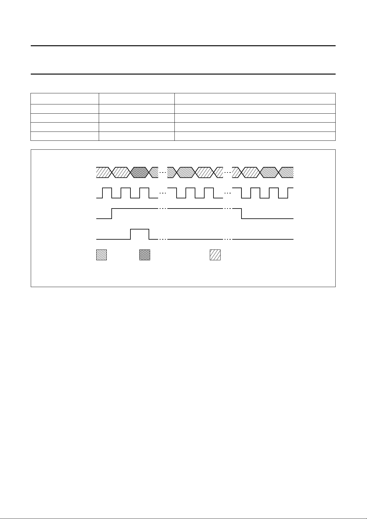
HE CODED DATA SLAVE INPUT INTERFACE
T
The coded data slave input interface signals are shown in
Fig.8. The coded data master input interface consists of
5 signals (see Table 8).
September 1994 14
Page 15

Philips Semiconductors Preliminary specification
MPEG Audio Source Decoder SAA2500
Table 8 Signals of coded data slave input interface.
SIGNAL DIRECTION FUNCTION
CDS input ISO/MPEG coded input data (slave input)
CDSEF input coded data (slave input) error flag
CDSCL input coded data (slave input) clock
CDSWA input coded data (slave input) burst windowing signal
CDSSY input coded data (slave input) frame sync
handbook, full pagewidth
CDS
CDSCL
CDSWA
CDSSY
CDSEF
valid data valid but unreliable data invalid data
CDSSY indicates frame start during valid data.
frame start
Fig.8 Input data serial transfer format (slave input).
CDS is the SAA2500 input data bitstream. Data clock
CDSCL must have a frequency equal to or higher than the
bit rate. The maximum CDSCL frequency is 768 kHz. Error
flag CDSEF is handled in the same way as CDMEF is
handled for the master input (in Fig.8, one unreliable data
bit is shown as an example). The value of CDSEF is
neglected for those bits where CDSWA is LOW. Window
signal CDSWA being HIGH indicates valid data; in this
way, burst input data is allowed. The constraints for the
ability to use ‘burst signals’ are explained below. Frame
sync signal CDSSY indicates the start of each input data
frame. CDSSY is synchronous with CDSCL. CDSSY may
be present or not: as described below. The first valid CDS
bit after a leading edge of CDSSY is interpreted to be the
first frame bit.
1 unreliable data bit (example)
MGB496
The minimum time for CDSSY to stay HIGH is one CDSCL
period; the maximum HIGH period is constrained by the
requirement that CDSSY must be LOW at least during one
CDSCL period per frame (a leading edge, i.e. a frame start
indication, must be present every frame). Leading edges
of CDSSY can occur while CDSWA is HIGH, as in Fig.8.
Alternatively, a situation as shown in Fig.9 is also allowed,
where CDSSY has a leading edge while CDSWA is LOW,
i.e. during invalid data. The first CDS bit after CDSWA
going HIGH is now interpreted to be the first frame bit.
September 1994 15
Page 16

Philips Semiconductors Preliminary specification
MPEG Audio Source Decoder SAA2500
handbook, full pagewidth
CDS
CDSCL
CDSWA
CDSSY
valid data invalid data
CDSSY indicates frame start at next valid data.
frame start
Fig.9 Input data serial transfer format (slave input).
Whether frame sync signal CDSSY is present or not must
be selected with L3 settings flags MSEL1 and MSEL0
(see Section “SAA2500 settings item”). With respect to the
presence of CDSSY, two situations can be distinguished:
1. If CDSSY is supplied, CDSWA may change each
CDSCL period.
2. If CDSSY is not supplied, CDSCL must have a
frequency higher than the bit rate (i.e. CDSWA
cannot be continuously HIGH), and CDSWA HIGH
periods may have only lengths of a multiple of
8 CDSCL periods: data is input in byte bursts.
Furthermore, these bursts must be byte aligned with
the frame bounds: frames are only allowed to start at
the 1st, 9th, 17th etc. bit in a valid data burst. For
applications where data is input in bursts of exactly
one frame, and where CDSCL has a higher frequency
than the bit rate, CDSWA and CDSSY may be
interconnected.
MGB497
It shows the transferring of nf bits in one frame between
time 0 and t, where t corresponds to 384 sample periods
(ISO/MPEG layer I input data) or 1152 sample periods
(ISO/MPEG layer II input data). Buffer margin B equals 16
bytes (128 bits). In Fig.10 an effective transferring
characteristic is drawn, representing any of the possible
ISO/MPEG bit rates. However, input data may be
transferred at a higher-than-effective speed (in other
words: CDSCL may have a higher frequency than the
effective bit rate) in periods during which CDSWA is HIGH,
interleaved with invalid data periods where CDSWA is
LOW. In the example of Fig.9 this is used to transfer the
data of the frame in two bursts, as shown by the actual
transferring characteristic. The actual transferring
characteristic has a slope equal to the CDSCL frequency
while CDSWA is HIGH, and is horizontal during the
periods in which CDSWA is LOW (no bits are being
transferred).
LAVE INPUT TRANSFER SPEED OF FIRST FRAME
S
Both the average and the instantaneous speed at which
data is transferred to the slave input interface are limited.
The data transferring of the first ISO/MPEG frame after
starting to decode is shown in Fig.10.
September 1994 16
Page 17

Philips Semiconductors Preliminary specification
MPEG Audio Source Decoder SAA2500
ndbook, full pagewidth
transferred
input frame bits
n
B
0
B
(1) The actual transferring characteristics of all frames are restricted to this area.
(2) Effective transferring characteristic (example).
(3) Actual transferring characteristic of the first frame (example).
slope: maximum
input bit rate
slope: CDSCL
frequency
(3)
Fig.10 Slave input data transferring for the first frame.
The shaded area in Fig.10 represents the restrictions to
the actual transferring characteristic of all frames. The
actual transferring characteristic may not undercut the
effective transferring characteristic by more than B bits to
avoid an input underflow. On the other hand, the actual
transferring characteristic may not cross the shown upper
limit of the shaded area to prevent an input buffer overflow.
The slope of this upper limit is determined by the maximum
effective input bit rate (depending on the input data
format). Table 9 summarizes the slopes as determined by
the bit rates supported by ISO/MPEG.
Table 9 Slopes determined by bit rates supported by
ISO/MPEG.
MGB498
(1)
B
B
slope: effective
input bit rate
(2)
t
time
SLAVE INPUT TRANSFER SPEED OF SUBSEQUENT FRAMES
The SAA2500 starts decoding as soon as enough data of
the first ISO/MPEG input data frame has been received.
Thus the start moment of decoding depends on the actual
transferring characteristic of the first frame. Decoding start
times of subsequent input data frames are also governed
by this initial start time.
For this reason the transferring characteristic of all
subsequent frames must approximate the characteristic of
the first frame within the buffer margin±B. For the example
shown in Fig.10, subsequent frames must be transferred
within the shaded area shown in Fig.11.
EFFECTIVE
ISO/MPEG
INPUT BIT
LAYER
(kbits/s)
ISO/MPEG layer I ±13.3
ISO/MPEG layer II 3.5
RATE
(1)
to 448 448
(1)
to 384 384
TRANSFERRING
UPPER LIMIT
SLOPE (kbits/s)
Note
1. Achieved using the free format option and the
minimum amount of the side information that must be
transmitted (this means using single channel mode, no
CRC and 32 kHz sample rate).
September 1994 17
Page 18

Philips Semiconductors Preliminary specification
MPEG Audio Source Decoder SAA2500
handbook, full pagewidth
transferred
input frame bits
n
B
0
B
(1) The actual transferring characteristics of all subsequent frames are restricted to this area.
(2) Effective transferring characteristic (example).
(3) Actual transferring characteristic of the first frame (example).
slope: CDSCL
frequency
(3)
Fig.11 Slave input data transferring for subsequent frames, referenced to the first frame.
Note that the actual transferring characteristics of all
frames must also remain inside the shaded area of Fig.11.
(1)
(2)
MGB499
B
B
slope: effective
input bit rate
t
time
The subband filter interface
As mentioned earlier, decoded signals in the subband
domain (before synthesis filtering) are available externally
2
for processing. The associated interface has an I
S-like
format (see Fig.12).
September 1994 18
Page 19

Philips Semiconductors Preliminary specification
MPEG Audio Source Decoder SAA2500
handbook, full pagewidth
TO
SCK
WS
WS
TB
left sample
MSB LSB
1
22526
TI
valid data undefinied data
subband
012 30 31 0 1
LRLR
24
32
MGB500
MSB
1
right sample
2
Fig.12 Filter data serial transfer format.
The filter data interface uses 6 signals as shown in Table 10.
Table 10 Signals of filter data interface.
SIGNAL DIRECTION FUNCTION
TO output filter data output
TA output filter data error flag
TI input filter data input (optionally processed)
SCK output filter data (output/input common) bit clock
WS output filter data (output/input common) word select
TB output filter data output frame synchronization
Two subband samples (one per channel) are transmitted
per sample period with output TO. The transmission
pattern of the samples S [sb, ch] (sb: subband index; ch:
channel) is: S [0, L], S [0, R], S [1, L], S [1, R],..., S [31, R],
S [0, L], S [0, R], etc. Word select signal WS indicates the
channel of each sample. (WS is also used for the
baseband audio output interfacing).
The subband sample bit clock SCK has a frequency of 64
times the sample frequency. The subband samples are
transmitted in 24 bit two's complement PCM form, MSB
first. Thus, of the available 32 TO bits per sample per
channel, only 24 are used. The MSB of a sample follows
one SCK period after each transition in WS. The
8 unused bits between individual samples in TO are zero.
(SCK is used for the baseband audio output interface as
well.) The optionally processed subband data signal is fed
back as input TI in a similar format as TO, but now the
8 unused bits between individual samples are undefined;
they are neglected by the SAA2500.
September 1994 19
Page 20

Philips Semiconductors Preliminary specification
MPEG Audio Source Decoder SAA2500
A leading edge in signal TB indicates the start of each TO
frame. The length of each TB pulse is one sample period;
TB is HIGH during a S[0,L] and S[0,R] pair. Signal TA
being HIGH indicates muting of TO due to input data errors
(see Fig.13).
TA can only change value at each TB leading edge, i.e.
after each 384 sample periods (ISO/MPEG layer I input
data) or 1152 sample periods (ISO/MPEG layer II input
data): only whole frames are marked to be correct or
muted. As shown in detail in Fig.13, transitions of TB and
TA take place one SCK period before a trailing edge of
WS.
The optionally processed subband data TI must be
synchronous to SCK and WS. Furthermore, the subband
handbook, full pagewidth
WS
TB
1234
index of the TI samples must be synchronised to TB: a
subband 0 sample pair must be input when TB is HIGH (as
shown in Fig.12). This means that the delay of the external
processing is allowed to be any integer multiple of
32 sample periods. If no external processing is to be
applied, TO must be input back directly to TI.
The baseband output interface
2
The decoded baseband audio data is output in an I
S-like
format (see Fig.14).
The output interfacing consists of 3 signals (see Table 11).
384 (layer I)
1152 (layer II) 1 2
TA
WS
TB
TA
SCK
WS
TB
TA
SCK
MGB501
Fig.13 Filter data error flag (TA) timing.
September 1994 20
Page 21

Philips Semiconductors Preliminary specification
MPEG Audio Source Decoder SAA2500
handbook, full pagewidth
SD
SCK
WS
valid data
left sample
MSB
1 16/18/20/22 32 1 16/18/20/22 32
Fig.14 Baseband output data serial transfer format.
Table 11 Signals of output interfacing.
SIGNAL DIRECTION FUNCTION
SD output baseband audio data
SCK output data clock
WS output word select
LSB MSB
information). In the programming sections a general
transfer protocol outline is presented. In
Section “SAA2500 L3 protocol enhancement options”
several optional protocol enhancements are given, which
on the one hand are less transparent from the applicant's
point of view, but on the other hand increase the efficiency
of the L3 interfacing.
right sample
LSB
MGB502
The frequency of clock SCK is 64 times the sample
frequency. (SCK is also used for the subband filter
interface).
The signal SD is the serial baseband audio data, sample
by sample (left/right interleaved. The left sample and the
right immediately following it form one stereo pair). 32 bits
are transferred per sample per channel. The samples are
transmitted in two's complement, MSB first. The output
samples are rounded to either 16, 18, 20 or 22 bit
precision, selectable by the host with L3 control interface
flags RND1 and RND0. The remainder of the
32 transferred bits per sample per channel are zero.
The word select signal WS indicates the channel of the
output samples (LOW if left, HIGH if right). (WS is used for
the subband filter interface as well.) If indicated in the
coded input data, de-emphasis filtering is performed
digitally on the output data, thus avoiding the need of
analog de-emphasis filter circuitry.
The L3 control interface
The SAA2500 uses the L3 protocol with the associated
bus as the control interface with an optional host
microcontroller (see Chapter “Appendix” for more
SIGNALS
L3
The L3 protocol uses 3 signals (see Table 12).
Table 12 Signals of L3 protocol.
SIGNAL DIRECTION FUNCTION
L3DATA input/output L3 interface serial data
L3CLK input L3 interface bit clock
L3MODE input L3 interface
address/data select
The signals operate according to the L3 protocol
description. After each device reset, the L3 interface of the
SAA2500 must be initialised and as a consequence, the
L3 interface cannot be used while the device reset signal
is activated.
L3
TRANSFER TYPES
The L3 protocol enables the reading and writing of control,
status and data. In the L3 protocol, the host first issues an
8 bit wide ‘operational address’ on L3DATA while keeping
L3MODE LOW. All devices connected to the L3 bus read
the operational address. Next, data transfers from or to the
September 1994 21
Page 22

Philips Semiconductors Preliminary specification
MPEG Audio Source Decoder SAA2500
host are done while keeping L3MODE HIGH. The devices with an L3 operational address differing from the issued one
must ignore these data transfers until the next operational address is issued. Only the device with an address equal to
the issued operational address performs the transfer.
The SAA2500 has the L3 operational address as shown in Table 13.
Table 13 L3 operational address.
76543210
0 1 1 0 0 0 DOM1
(1)
Note
1. The ‘Data Operation Mode’ bits DOM1 and DOM0 determine the mode in which the SAA2500 L3 interface will stay
until the next time an L3 operational address is issued (see Table 14).
DOM0
(1)
Table 14 DOM1 and DOM0 bits.
DOM1 DOM0 TRANSFER TYPE
0 0 write item data
0 1 read item data
1 0 write control to SAA2500
1 1 read SAA2500 status
Control bytes can be written to the SAA2500.
Data is transferred to or from the SAA2500 in so-called
data items. The items can be a readable or writeable type.
A data item transfer is initiated by writing the
corresponding control byte to the SAA2500 first. Next, the
handbook, full pagewidth
RESET
L3MODE
L3CLK
item data itself is transferred, always as an integer number
of bytes.
The status of the SAA2500 can be read via L3. The
SAA2500 status flag L3RDY must be monitored before
transferring data item bytes to avoid transferring bytes
faster than the L3 interface of the SAA2500 can handle.
INTERFACE INITIALISATION AT AN SAA2500 DEVICE RESET
L3
Figure 15 shows the mandatory actions that must be taken
for correct L3 interface start-up at a device reset.
12 3
Fig.15 L3 interface initialisation procedure.
September 1994 22
MGB503
Page 23

Philips Semiconductors Preliminary specification
MPEG Audio Source Decoder SAA2500
The actions shown in Fig.15 are:
1. In order for the SAA2500 to keep L3DATA in 3-state,
L3MODE must be kept LOW during the whole period
that reset signal RESET is asserted; meanwhile, no
transfers can be performed (L3CLK stays HIGH).
2. For a proper initialisation of the L3 interface logic of the
SAA2500, it is mandatory to make L3MODE HIGH and
LOW again after the device reset has been
de-activated. This must be done before any L3
transfer, even to or from other devices than the
SAA2500, is performed. Figure 14 shows that L3CLK
stays HIGH during this step.
3. Now the first transfer can be performed on the L3 bus.
This transfer must be a operational address (indicated
in Fig.14 by L3MODE = 0), addressing any of the
devices connected to the L3 bus. The first transfer to
Table 15 L3 control.
76543210
CTRL7 CTRL6 CTRL5 CTRL4 CTRL3 CTRL2 CTRL1 CTRL0
The definitions of the control bytes (CTRL7 to CTRL0) are given in Table 16.
the SAA2500 itself must always be either the writing of
a control word or the reading of the SAA2500 status;
the first transfer may never be a data item byte
transfer.
Remark: any deviation from these steps may result in
illegal L3 protocol behaviour of the SAA2500, even with
the possibility of disturbing transfers to other devices
connected to the L3 bus.
INTERFACE CONTROL
L3
The control of the SAA2500 L3 interface is performed with
one-byte control words. Status polling is not necessary
before writing control bytes. After writing the SAA2500
‘write control’ operational address, one or more control
bytes may be written. Each written control byte overrules
the previously sent control byte.
Table 16 Explanation of control bytes
CTRL7 TO CTRL0 DEFINITION TYPE
00000000 read/write SAA2500 settings item I
00000001 read decoded frame header item I
00000010 read used frame header item I
00000011 read error report item I
00000100 reserved I
00000101 read ancillary Data item I
00000110 write APU coefficients item I
00000111 continue previous transfer C
00001000 to 11111111 reserved −
Note
1. Control bytes of type I initiate the transfer of a data item. The control byte of type C may be used after interrupting a
transfer, in order to write APU coefficients, to return to the interrupted transfer.
SAA2500 STATUS
The host can check the status of the SAA2500 by reading
the one-byte status word. After writing the SAA2500 ‘read
status’ operational address, the status byte may be read
an arbitrary number of times. If status is read more than
once, it is updated by the SAA2500 between the individual
readings. The status flags of the SAA2500 have the
definition as shown in Table 17.
(1)
September 1994 23
Page 24

Philips Semiconductors Preliminary specification
MPEG Audio Source Decoder SAA2500
Table 17 Status flag definitions.
76543210
(1)
DST2
Notes
1. By interpreting DST2 to DST0, the host can synchronize to the input frame frequency, and also determine at which
moment which L3 data item is available to be read. The value of DST2 to DST0 is only valid if flag INSYNC is set.
a) DST2 is a modulo 2 frame counter, i.e. DST2 inverts at the moment the decoding of a new frame is started. DST2
enables to host to sample the decoding subprocess DST1 to DST0 less frequently, meanwhile enabling the host
to see if it missed a state.
b) DST1 and DST0 values are explained in Table 18.
2. INSYNC is synchronization indication:
a) INSYNC = 0; the SAA2500 is not synchronized to the input data.
b) INSYNC = 1; the SAA2500 is synchronized to the input data.
3. As indicated in Section “Input data frame header items”, some of the readable data item bits only have significance
if INSYNC = 1.
4. L3RDY is L3 interface ready indication:
a) L3RDY = 0; the L3 interface cannot perform a new item data transfer yet.
b) L3RDY = 1; the L3 interface is ready for the next item data transfer.
After a device reset, L3RDY is cleared and will only become set after writing the first L3 control byte to the SAA2500.
The value of L3RDY can be tested by polling signal L3DATA instead of transferring the whole status byte.
DST1
(1)
DST0
(1)
undefined undefined undefined INSYNC
(2)(3)
L3RDY
(4)
Table 18 Status bytes DST1 and DST0.
DST1 DST0 FUNCTION
0 0 subprocess 0; reading Ancillary Data or decoding header
0 1 subprocess 1; decoding bit allocation or scale factor select information
1 0 subprocess 2; decoding scale factors
1 1 subprocess 3; decoding samples
The DST1 and DST0 values in general do not have a determined duration. However, subprocess 3 takes at least a
1
⁄2frame period when ISO/MPEG layer I data is decoded, and5⁄6frame period when ISO/MPEG layer II data is decoded.
Table 19 indicates the validity of the SAA2500 readable data items with respect to the decoding subprocess. Reading of
a data item in a period when it is not valid renders undefined data.
September 1994 24
Page 25

Philips Semiconductors Preliminary specification
MPEG Audio Source Decoder SAA2500
Table 19 Validity of SAA2500 readable data items with respect to the decoding subprocess (notes1and2).
SAA2500 IS DECODING FRAME n SAA2500 IS DECODING FRAME n + 1
DST2 = 0 DST2 = 1
DST1 AND
DST0 = 0
not valid Ancillary Data item (frame n − 1) not valid −−−
−not valid error report: BALOK (frame n) not valid −−
− not valid error report: DECFM
Notes
1. The Table shows following:
a) The received Ancillary Data that was multiplexed in frame n−1 becomes valid after subprocess 0 of frame n, and
may be read during subprocesses 1, 2 and 3 of frame n.
b) The decoded and used frame headers for frame n become valid after subprocess 0 of frame n, and may be read
during subprocesses 1, 2 and 3 of frame n.
c) Flag BALOK for frame n in the error report item becomes valid after subprocess 1 of frame n, and may be read
during subprocesses 2 and 3 of frame n and subprocess 0 of frame n+1.
d) Flag DECFM for frame n in the error report item becomes valid after subprocess 2 of frame n, and may be read
during subprocesses 3 of frame n and 0 of frame n+1.
2. Note that during subprocess 3 all data items can be read.
DATA ITEMS
Data can be transferred to or from the SAA2500 in data
items. This section describes the general protocol to
accomplish item data transfer, followed by the individual
SAA2500 data items. Optional enhancements on the
general protocol are described in Chapter “Appendix”
Section “SAA2500 L3 protocol enhancement options”.
General data items
The data items of the SAA2500 are transferred (i.e. read
or written, depending on whether the data item is of
readable or writeable type) in bytes. A data item transfer is
DST1 AND
DST0 = 1
frame header items (frame n) −−−
DST1 AND
DST0 = 2
DST1 AND
DST0 = 3
(frame n)
DST1 AND
DST0 = 0
initiated by writing the corresponding type I control byte
(see Section “L3 interface control”) to the SAA2500. The
transfer of every subsequent item data byte must be
preceded by reading the status until status flag L3RDY
(see Section “SAA2500 status”) is HIGH.
L3RDY may be tested alternatively by polling L3DATA,
avoiding the need to transfer the whole status byte. Status
polling is not required while transferring the APU
coefficients item. Table 20 shows an example of how
bytes ‘DDDDDDDD’ of a 2 byte data item, with the
corresponding control byte ‘CCCCCCCC’, can be read.
The writing of item data bytes occurs in a similar way.
DST1 AND
DST0 = 1
DST1 AND
DST0 = 2
not valid −
DST1 AND
DST0 = 3
September 1994 25
Page 26

Philips Semiconductors Preliminary specification
MPEG Audio Source Decoder SAA2500
Table 20 Example of a 2 byte data item.
L3DATA
01100010 host 0 1; indicates ‘write control’ transfer
CCCCCCCC host 1 2; write transfer initiating (type I) control byte
01100011 host 0 3; indicates ‘read status’ transfer
SSSSSSSS SAA2500 1 4; read status (repeat step 4 until L3RDY = 1)
01100001 host 0 5; indicates ‘read item data’ transfer
DDDDDDDD SAA2500 1 6; read first item data byte
01100011 host 0 7; indicates ‘read status’ transfer
SSSSSSSS SAA2500 1 8; read status (repeat step 8 until L3RDY = 1)
01100001 host 0 9; indicates ‘read item data’ transfer
DDDDDDDD SAA2500 1 10; read second item data byte
Each data item has its own length in bytes. It is allowed to transfer less bytes than the data item length, skipping the last
one or more bytes (it is even allowed to transfer no bytes at all). It is not allowed to transfer more bytes than the item
length. This restriction does not hold for the APU coefficient item. After writing all APU coefficients (i.e. after writing all
APU coefficient item bytes), they may be rewritten by continuing writing bytes to the APU coefficient item. Writing more
than the specified number of bytes to a writeable data item or writing bytes to a read-only data item may cause the
SAA2500 to malfunction. The reading of a write-only data item yields irrelevant data.
TRANSFER
SOURCE
L3MODE EXPLANATION
September 1994 26
Page 27

Philips Semiconductors Preliminary specification
MPEG Audio Source Decoder SAA2500
SAA2500 SETTINGS ITEM
The SAA2500 is configured with the SAA2500 settings. The initial value of the SAA2500 settings after reset is all zeros.
Table 21 SAA2500 settings item; 1 byte (read/write).
76543210
MSEL1
(1)
MSEL0
Notes
1. MSEL1 and MSEL0; these bits select the used input interface, the input data format and the input synchronization
type (see Table 22).
2. CRCACT; automatic/forced CRC activity:
a) CRCACT = 0; the SAA2500 uses the protection bit in the ISO/MPEG frame header to determine the presence of
the CRC.
b) CRCACT = 1; the SAA2500 assumes the CRC always to be present. The protection bit in the used ISO/MPEG
frame header is forced to 0.
3. MCKDIS; buffered master clock MCLK disabling:
a) MCKDIS = 0; enable MCLK.
b) MCKDIS = 1; disable (3-state) MCLK.
4. FCKENA; buffered 256f
a) FCKENA = 0; disable (3-sate) FSCLK.
b) FCKENA = 1; enable FSCLK.
5. SELCH2; with dual channel mode input data (with other modes of input data ‘don’t care’:
a) SELCH2 = 0; select channel I.
b) SELCH2 = 1; select channel II.
6. RND1 and RND0; these bits select the rounding of the baseband audio output samples (see Table 23).
(1)
CRCACT
or 384fs output signal FSCLK enabling:
s
(2)
MCKDIS
(3)
FCKENA
(4)
SELCH2
(5)
RND1
(6)
RND0
(6)
Table 22 MSEL1 and MSEL0.
MSEL1 MSEL0 USED INPUT INTERFACE INPUT SYNCHRONIZATION
0 0 master to ISO/MPEG synchronization pattern
0 1 reserved reserved
1 0 slave to ISO/MPEG synchronization pattern
1 1 slave to synchronization signal CDSSY
Table 23 RND1 and RND0.
RND1 RND0 OUTPUT SAMPLE ROUNDING LENGTH
0 0 16 bits
0 1 18 bits
1 0 20 bits
1 1 22 bits
September 1994 27
Page 28

Philips Semiconductors Preliminary specification
MPEG Audio Source Decoder SAA2500
INPUT DATA FRAME HEADER ITEMS
Information about the input data, derived by the SAA2500 from the input data frame headers, may be read from the frame
header items. Both the frame header bytes decoded from the input bitstream and the header bytes used for the actual
decoding may be read.
The decoded frame header item is valid independent of the value of status flag INSYNC, it e.g. shows the decoded
headers while the SAA2500 is in the process of synchronising.
The used frame header item is only valid if status flag INSYNC is set. The used header bytes are derived by the SAA2500
from the decoded header bytes by overruling NOPROT to 0 if settings bit CRCACT = 1, and overruling detected errors.
Table 24 Decoded input data frame header item; 3 bytes (read-only).
SUBSEQUENT
BYTES
Decoded header
765432 1 0
SY3
(1)
SY2
(1)
SY1
(1)
SY0
(1)
ID
(2)
LAY1
(3)
LAY0
(4)
NOPR
(5)
byte 1
Decoded header
BR3
(6)
BR2
(6)
BR1
(6)
BR0
(6)
FS1
(7)
FS0
(7)
undefined undefined
byte 2
Decoded header
MOD1
(8)
MOD0
(8)
MODX1
(9)
MODX0
(9)
COPR
(10)
ORIG
(11)
EMPH1
(12)
EMPH0
(12)
byte 3
Notes to Tables 24 and 25
1. SY3 to SY0; last 4 bits of the synchronization word.
2. ID; algorithm identification.
3. LAY1; layer Most Significant Bit (MSB).
4. LAY0; layer Least Significant Bit (LSB).
5. NOPR; CRC on header, bit allocation and scale factor select information activity flag.
6. BR3 to BR0; bit rate index.
7. FS1 and FS0; sample rate index.
8. MOD1 and MOD0; mode.
9. MODX1 and MODX0; mode extension.
10. COPR; copyright flag.
11. ORIG; original or home copy flag.
12. EMPH1 and EMPH0; audio de-emphasis, these bits are only meant to monitor the current de-emphasis mode; the
corresponding de-emphasis is performed by the SAA2500 automatically before the baseband audio signal is output.
Table 25 Used input data frame header item; 3 bytes (read-only).
SUBSEQUENT BYTES 7654321 0
Used header byte 1 111111LAY0NOPR
Used header byte 2 BR3 BR2 BR1 BR0 FS1 FS0 undefined undefined
Used header byte 3 MOD1 MOD0 MODX1 MODX0 COPR ORIG EMPH1 EMPH0
RROR REPORT ITEM
E
The validity of bit allocation plus scale factor select information may be read from the error report item. The error report
item is only valid if status flag INSYNC is set.
September 1994 28
Page 29

Philips Semiconductors Preliminary specification
MPEG Audio Source Decoder SAA2500
Table 26 Error report item; 1 byte (read-only).
SUBSEQUENT
BYTES
Error report BALOK
76543210
(1)
DECFM
(2)
undefined undefined undefined undefined undefined undefined
Notes
1. BALOK; bit allocation and scale factor select information validity indication:
a) BALOK = 0; bit allocation or scale factor select information are incorrect, or the CRC (if active) over header, bit
allocation and scale factor select information fail.
b) BALOK = 1; bit allocation or scale factor select information are correct, and the CRC (if active) over header, bit
allocation and scale factor select information passes.
2. DECFM; frame skipping/decoding indication:
a) DECFM = 0; the current input data frame is skipped, and the corresponding baseband audio output frame is
muted due to input data errors or inconsistencies. However, synchronization to the input data is maintained.
b) DECFM = 1; the current frame is decoded normally.
NCILLARY DATA ITEM
A
The last 54 bytes of each ISO/MPEG frame, which may carry Ancillary Data (AD), are buffered by the SAA2500 to be
read by the host. The subsequent Ancillary Data bytes are read in reversed order with respect to their order in the input
data bitstream. The first item data byte is the last frame byte in the input bitstream. The Ancillary Data item is refilled at
every frame. The host must either know or determine itself how many of the Ancillary Data bytes are valid per frame. The
Ancillary Data item only has significance if status flag INSYNC is set.
Table 27 Ancillary data item; 54 bytes (read-only).
SUBSEQUENT
BYTES
AD byte 1 to
76543210
bit 7 bit 6 bit 5 bit4 bit 3 bit 2 bit 1 bit 0
AD byte 54
COEFFICIENTS ITEM
APU
The APU coefficients are set by writing their 8 bit indices to the 4-byte APU coefficient item. Only the 7 LSBs are valid.
The MSB must be zero. At a device reset, indices LL and RR are set to 00000000 (‘no attenuation’) and indices LR and
RL to 01111111 (infinite attenuation; no crosstalk).
Table 28 APU coefficients item; 4 bytes (write-only); see note 1.
SUBSEQUENT
BYTES
76543210
APU coefficient LL 0 LL.6 LL.5 LL.4 LL.3 LL.2 LL.1 LL.0
APU coefficient LR 0 LR.6 LR.5 LR.4 LR.3 LR.2 LR.1 LR.0
APU coefficient RL 0 RL.6 RL.5 RL.4 RL.3 RL.2 RL.1 RL.0
APU coefficient RR 0 RR.6 RR.5 RR.4 RR.3 RR.2 RR.1 RR.0
Note
1. Multiple options are supplied by the SAA2500 to increase the timing accuracy of the APU coefficient writing
(see Section “SAA2500 L3 protocol enhancement options”).
September 1994 29
Page 30

Philips Semiconductors Preliminary specification
MPEG Audio Source Decoder SAA2500
SPEED LIMITATIONS OF THE L3 INTERFACE
When reading the status of, or writing control bytes to the
SAA2500, no status polling is necessary, so the speed of
these transfers is only limited by the maximum frequency
of signal L3CLK and the timing constraints of the L3
protocol.
DEFAUL T ITEM DATA VALUES AFTER RESET
At a device reset, the L3 interface initialisation procedure
must be followed. All writeable data items are pre-loaded
with a defined default value after the device reset signal
has been de-activated. These default values are
summarised in Table 29.
When reading or writing data item bytes, status polling is
necessary. In addition to the speed limitation this poses,
the application must take precautions that individual data
item bytes are transferred at an interval of at least 200 µs.
Neither the status polling nor a minimum interval between
transfers is required when transferring the APU coefficient
item.
Table 29 SAA2500 settings item; default value after device reset (notes 1 to 6.)
SUBSEQUENT
BYTES
76543210
SAA2500 settings MSEL1 MSEL0 CRCACT MCKDIS FCKENA SELCH2 RND1 RND0
Value 0 0 0 0 0 0 0 0
Notes
1. MSEL1 = 0 and MSEL0 = 0; the master input is selected. The SAA2500 synchronizes to the ISO/MPEG
synchronization pattern.
2. CRCACT = 0; the SAA2500 uses the protection bit in the ISO/MPEG frame header to determine if the CRC is active.
3. MCKDIS = 0; the buffered master clock output MCLK is enabled.
4. FCKENA = 0; the buffered 256f
or 384fs clock output is disabled.
s
5. SELCH2 = 0; when decoding input data with dual channel mode, channel I is output on both baseband audio output
channels.
6. RND1 = 0 and RND0 = 0; the baseband audio output signals are rounded to 16 bit.
Table 30 APU coefficients item; default values after device reset.
SUBSEQUENT
BYTES
APU coefficient LL
APU coefficient LR
APU coefficient RL
APU coefficient RR
(1)
(2)
(3)
(4)
76543210
0 LL.6 = 0 LL.5 = 0 LL.4 = 0 LL.3 = 0 LL.2 = 0 LL.1 = 0 LL.0 = 0
0 LR.6 = 1 LR.5 = 1 LR.4 = 1 LR.3 = 1 LR.2 = 1 LR.1 = 1 LR.0 = 1
0 RL.6 = 1 RL.5 = 1 RL.4 = 1 RL.3 = 1 RL.2 = 1 RL.1 = 1 RL.0 = 1
0 RR.6 = 0 RR.5 = 0 RR.4 = 0 RR.3 = 0 RR.2 = 0 RR.1 = 0 RR.0 = 0
Notes
1. LL = 00000000; no attenuation in the left-to-left APU path.
2. LR = 01111111; infinite attenuation in the left-to-right APU path.
3. RL = 01111111; infinite attenuation in the right-to-left APU path.
4. RR = 00000000; no attenuation in the right-to-right APU path.
September 1994 30
Page 31

Philips Semiconductors Preliminary specification
MPEG Audio Source Decoder SAA2500
APPENDIX
Preliminary specification 3-line ‘L3’ interface
NTRODUCTION
I
The main purpose of the new interface definition is to
define a protocol that allows for the transfer of control
information and operational details between a
microcontroller (µC) and a number of slave devices, at a
rate that exceeds other common interfaces, but with a
sufficient low complexity for application in consumer
products. It should be clearly noted that the current
interface definition is intended for use in a single
apparatus, preferably restricted to a single printed circuit
board.
The new interface requires 3 signal lines (apart from a
return ‘ground’) between the microcontroller and the slave
devices (from this the name ‘L3’ is derived). These 3-lines
are common to all ICs connected to the bus: L3MODE,
L3DATA and L3CLK. L3MODE and L3CLK are always
driven by the microcontroller, L3DATA is bidirectional:
Table 31 The 3-lines common to all ICs; L3MODE,
L3CLK and L3DATA.
SIGNAL MICROCONTROLLER
(1)
L3MODE
L3CLK
L3DATA
output input
(2)
output input
(3)
output/input input/output
SLAVE
DEVICE
Notes
1. L3MODE is used for the identification of the operation
mode.
2. L3CLK is the bitclock to which the information transfer
will be synchronized.
3. L3DATA will carry the information to be transferred.
All slave devices in the system can be addressed using a
6 bit address. This allows for up to 63 different slave
devices, as the all ‘0’ address is reserved for special
purposes. In addition it is possible to extend the number of
addressable devices using ‘extended addressing’.
In operation 2 modes can be identified:
1. Addressing mode (AM).
During addressing mode a single byte is sent by the
microcontroller. This byte consists of 2 data operation
mode (DOM) bits and 6 operational address (OA) bits.
Each of the slave devices evaluates the operational
address. Only the device that has been issued the
same operational address will become active during
the following data mode. The operation to be executed
during the data mode is indicated by the two data
operation mode bits.
2. Data mode (DM).
During data mode information is transferred between
microcontroller and slave device. The transfer
direction may be from microcontroller to slave (‘write’)
or from slave to microcontroller (‘read’). However,
during one data mode the transfer direction can not
change.
Addressing mode
In order to start an addressing mode the microcontroller
will make the L3MODE line LOW. The L3CLK line is
lowered 8 times and the DATA line will carry 8 bits. The
addressing mode is ended by making the L3MODE line
HIGH.
September 1994 31
Page 32

Philips Semiconductors Preliminary specification
MPEG Audio Source Decoder SAA2500
handbook, halfpage
L3MODE
L3CLK
L3DATA
The meaning of the bits on L3DATA.
Bit 0 and bit 1; these are the data operation mode (DOM) bits that indicate the nature of the following data transfer. Each slave device may have
its own allocation of operation modes to the 4 possible codes of these bits. For correct information about the operation the device will perform, refer
to the descriptions of the individual IC's. For new designs the preferred allocations are given in Table 32.
Bit 2 to bit 7; these bits act as 6 bit (special function) operational IC address, with bit7 as MSB and bit 2 as LSB. Bit7 tobit 5 act as system
identification and bit 4 to bit2 as identification of the device within the system.
01234567
MGB505
Fig.16 Addressing mode.
Table 32 Preferred allocations.
DOM1 DOM0 FUNCTION REMARKS
0 0 data from microcontroller to SAA2500 general purpose data transfer
0 1 data from SAA2500 to microcontroller general purpose data transfer
1 0 control from microcontroller to SAA2500 e.g. register selection for data transfer
1 1 status from SAA2500 to microcontroller short device status message
Special function operational address
Operational address 000000 (bit 2 to bit 7) is the special
function address, and is used for the L3 device reset, as
well as for the declaration and invalidation of the extended
addressing. Both will be explained in Sections “Device
interface reset” and “Extended addressing”.
transfer the L3MODE line is HIGH. The L3CLK line is
lowered 8 times during which the L3DATA line carries
8 bits. The information is presented LSB first and remains
stable during the LOW phase of the L3CLK signal.
The preferred basic data transfer unit is an 8 bit byte.
Some implementations that are modifications of older
circuits with 16 bit registers may use a basic unit of 16 bits,
Data mode
In the data mode the microcontroller sends or receives
transferred as 2 bytes, with the most significant byte
presented first. No other basic data transfer unit is allowed.
information to or from the selected device. During data
September 1994 32
Page 33

Philips Semiconductors Preliminary specification
MPEG Audio Source Decoder SAA2500
Halt mode
handbook, halfpage
L3MODE
L3CLK
L3DATA
01234567
Fig.17 Data transfer mode.
In between units the L3MODE line will be driven LOW by
the microcontroller to indicate the completion of a basic
unit transfer. This is called ‘halt mode’ (HM). During halt
mode the L3CLK line remains HIGH (to distinguish it from
an addressing mode). The halt mode allows an
implementation of an interface module without a bit
counter. However, an implementation using a bit counter
in the interface module may allow for the L3MODE line to
be kept HIGH in between units (not using the halt mode).
This implementation must also operate correctly if the halt
mode is used. The documentation of the device will have
to indicate clearly whether or not the ‘halt mode’ is
necessary for correct operation of the interface.
EVICE INTERFACE RESET
D
If the microcontroller sends an operational address
‘000000’ with DOM1 and DOM0 also equal to ‘0’ this
indicates that none of the L3 interface devices is allowed
to communicate with the microcontroller during the
following data mode. This enables a different application of
the L3CLK and L3DATA lines as the L3 devices will not
MGB504
interfere with any communication on these lines as long as
L3MODE remains HIGH (e.g. the L3CLK and L3DATA
lines are normally connected to USART circuits in the
microcontrollers which allow for convenient
communication between microcontrollers).
Any addressing mode with a valid L3 operational address
will re-enable the communication with the corresponding
device.
Devices with a fixed operational address (‘Primary L3
devices’) will react with a device reset condition regardless
of the state of DOM1 and DOM0.
Devices with a programmable operational address
(‘Secondary L3 devices’) can only be put in the interface
reset condition if the DOM1 and DOM0 bits are ‘0’. Other
combinations of DOM1 and DOM0 initiate data transfers
for ‘extended addressing’.
E
XTENDED ADDRESSING
L3 Devices with a programmable address can be informed
of their operational address using a special data transfer.
September 1994 33
Page 34

Philips Semiconductors Preliminary specification
MPEG Audio Source Decoder SAA2500
Operational address declaration
For the declaration (programming) of the operational
address of an L3 device with a ‘secondary L3 identification
code’ the following action is required:
1. First the microcontroller must issue an L3 operational
address ‘000000’ (special function address) with
DOM1 = 0 and DOM0 = 1. This combination defines
the operational address declaration operation. Next
the microcontroller will start a data transfer mode in
which it first sends the secondary L3 identification
code for the device that is to be issued an operational
address, followed by a byte containing the operational
address (the DOM bits in this byte are don't cares).
2. Next the microcontroller will start a data transfer mode
in which it first sends the secondary L3 identification
code for the device that is to be issued an operational
address, followed by a byte containing the operational
address (the DOM bits in this byte are don't cares).
A secondary L3 identification code is unique for any
design. Devices of the same design have the same
identification code of one or more bytes. However, special
Table 33 Example of L3 devices; notes 1 to 4.
designs may have a range of identification codes, one of
which can be selected by a hardware solution, to enable
the connection of more than one device of the same
design to the L3 interface. It is also possible to use
separate L3MODE lines for multiple devices of the same
design, but the same L3 identification code (this also
enables ‘parallel programming’ of these devices). Bit 0 of
any identification code byte will indicate whether or not an
additional byte follows:
Bit 0 = 0; no additional byte as part of the identification
code.
Bit 0 = 1; additional byte follows.
With this the number of secondary L3 identification codes
is (theoretically) unlimited.
The operational address for the programmable device is
preferable in the range 111000 to 111111. However, it is
possible in a given application to issue any operational
address that is not used to address primary L3 devices or
other secondary L3 devices. An example is given in
Table 33.
ADDRESSING MODE DATA MODE
SECONDARY L3 IDENTIFICATION CODE OPERATIONAL
SPECIAL ADDRESS
10000000 1XXXXXXX 1XXXXXXX 0XXXXXXXX MMYYYYYY
Notes
1. Bits are shown in the order they appear on L3DATA (bit 0 first, bit 7 last).
2. X = bit of the identification code.
3. M = DOM bit of operational address (don’t care).
4. Y = bit of the operational address.
Operational address invalidation
In order to re-allocate an operational address that has
been allocated to a secondary L3 device it is possible to
invalidate an operational address:
• First the microcontroller must issue an L3 operational
address ‘000000’ (special function address) with
DOM1 = 1 and DOM0 = 0. This combination defines the
operational address invalidation operation.
• Next the microcontroller will start a data transfer mode in
which it only sends the secondary L3 identification code
for the device that will no longer be addressed. From this
BYTE 1 BYTE 2 BYTE 3
moment on the device will not be able to communicate
with the microcontroller until it is issued a new
operational address by an OA declaration (it will enter a
‘device interface reset’ condition).
Remark: the combination of a special function address
(000000) and DOM1 and DOM0 equal to ‘1’ is reserved for
future applications. Designs based on this specification will
react with a ‘device interface reset’.
ADDRESS
(ONE BYTE)
September 1994 34
Page 35

Philips Semiconductors Preliminary specification
MPEG Audio Source Decoder SAA2500
EXAMPLE OF A DATA TRANSFER
handbook, full pagewidth
L3MODE
(1)
L3CLK
(2)
L3DATA
address
(1) L3CLK is triggered by L3MODE.
(2) For more details see Fig.20.
data
byte 1
byte 2
Fig.18 Example of transfer of 4 bytes.
A data transfer starts when the microcontroller sends an
address on the bus. All ICs will evaluate this address, but
only the IC addressed will be an active partner for the
microcontroller in the following data transfer mode.
During the data transfer mode bytes will be sent from or to
the microcontroller. In this example the L3MODE line is
made LOW (‘halt mode’) in between byte transfers. This is
the default operation, although some ICs may allow the
L3MODE line to be kept HIGH. This exception must be
specified clearly in the IC documentation, and such ICs
must be able to communicate with microcontrollers that
Addressing mode
data
data
byte 3
data
byte 4
address
MGB506
make L3MODE LOW in between transfers. It is suggested
that new designs only use bytes as basic data transfer
units. After the data transfer the microcontroller does not
need to send a new address until a new data transfer is
necessary. Alternatively it may also send the ‘special
address’ 000000 to indicate the end of the data transfer
operation.
IMING REQUIREMENTS
T
These are requirements for the slave devices designed
according to the 'L3' interface definitions.
t
handbook, full pagewidth
L3MODE
L3CLK
L3DATA
d1 h2
t
cL
t
cH
t
h1
t
su
Fig.19 Timing (addressing mode).
September 1994 35
t
MGB507
Page 36

Philips Semiconductors Preliminary specification
MPEG Audio Source Decoder SAA2500
Table 34 Requirements for timing (addressing mode); see Fig.19.
SYMBOL PARAMETER REQUIREMENT UNIT
t
d1
t
cL
t
cH
t
su1
t
h1
t
h2
Data mode
L3CLK HIGH to L3CLK LOW delay time after L3MODE LOW ≥190 ns
L3CLK LOW time ≥250 ns
L3CLK HIGH time ≥250 ns
L3DATA set-up time before L3CLK HIGH ≥190 ns
L3DATA hold time after L3CLK HIGH ≥30 ns
L3CLK hold time before L3MODE HIGH ≥190 ns
ndbook, full pagewidth
L3MODE
L3CLK
L3DATA
microcontroller
to IC
L3DATA
IC to
microcontroller
t
d1 h2
t
cL
t
d2
t
d3
t
cH
t
su
t
h1
t
h3
t
d4
t
t
d5
MGB508
Fig.20 Timing (data mode).
Table 35 Requirements for timing (data mode); see Fig.20.
SYMBOL PARAMETER REQUIREMENT UNIT
t
d1
t
cL
t
cH
L3CLK HIGH to L3CLK LOW delay time after L3MODE HIGH ≥190 ns
L3CLK LOW time ≥250 ns
L3CLK HIGH time ≥250 ns
Microcontroller to slave device
t
t
t
su1
h1
h2
L3DATA set-up time before L3CLK HIGH ≥190 ns
L3DATA hold time after L3CLK HIGH ≥30 ns
L3CLK hold time before L3MODE HIGH ≥190 ns
Slave device to microcontroller
t
d2
t
d3
t
h3
t
d4
t
d4
L3DATA enable time after L3MODE HIGH 0 < td2≤ 50 ns
L3DATA stable time after L3MODE HIGH ≤380 ns
L3DATA hold time after L3CLK HIGH ≥50 ns
L3DATA stable time after L3CLK HIGH ≤360 ns
L3DATA stable time after L3CLK HIGH between bit 7 of a byte and
≤530 ns
bit 0 of next byte if no halt mode is used
t
d5
L3DATA disable time after L3MODE LOW 0 < td5≤ 50 ns
September 1994 36
Page 37

Philips Semiconductors Preliminary specification
MPEG Audio Source Decoder SAA2500
Halt mode
t
handbook, full pagewidth
L3MODE
L3CLK
L3DATA
IC to
microcontroller
t
h2
t
d5
Fig.21 Timing (halt mode).
L
t
d1
t
d2
MGB509
Table 36 Requirements for timing (halt mode); see Fig.21.
SYMBOL PARAMETER REQUIREMENT UNIT
t
d1
t
L
t
h2
L3CLK HIGH to L3CLK LOW delay time after L3MODE HIGH ≥190 ns
L3MODE LOW time ≥190 ns
L3CLK hold time before L3MODE LOW ≥190 ns
Slave device to microcontroller
t
d2
t
d5
SAA2500 L3 protocol enhancement options
The L3 interface on the SAA2500 is limited in speed,
dictated both by the maximum SAA2500 handling speed
and the upper frequencies of the L3 interfacing standard.
On the other hand, the SAA2500 offers several
enhancements, described in this section, to make a better
use of the SAA2500 L3 interface capacity. The
enhancements are optional. The applicant chooses
whether to use them or not.
ESTING L3RDY BY POLLING L3DATA
T
L3DATA enable time after L3MODE HIGH 0 < td2≤ 50 ns
L3DATA disable time after L3MODE LOW 0 < td5≤ 50 ns
SAA2500 ‘read status’ operational address, after which
the status byte can be transferred. To avoid these status
byte transfers (thus reducing the host's load), after writing
the SAA2500 ‘read status’ operational address, L3RDY is
continuously copied to signal L3DATA during the period in
which no L3 transfers (i.e. status byte readings) are
performed. Meanwhile, L3MODE must be kept HIGH (no
L3 operational addresses may be written). As a result,
L3RDY can be tested as shown in Table 37.
The host must test status flag L3RDY to make sure
whether the SAA2500 L3 interface is ready to transfer data
item bytes. According to the general protocol, described in
Section “Data items”, the status is read by first writing the
September 1994 37
Page 38

Philips Semiconductors Preliminary specification
MPEG Audio Source Decoder SAA2500
Table 37 Status bytes DST1 and DST0; note 1.
L3DATA
01100011 host 0 write ‘read status’ operational address
polled SAA2500 1 test L3DATA; repeat this step until L3DATA = 1
Note
1. No status byte transfers are needed; the load of the host (microcontroller) can thus be reduced.
OPTIONS TO INCREASE THE TIMING ACCURACY OF THE APU
COEFFICIENT WRITING
The SAA2500 offers three enhancements to increase the
timing accuracy with which APU coefficients can be
updated by the application:
1. Status polling is not required when APU coefficients
are written. L3 status flag L3RDY, when read anyhow,
will always be HIGH, indicating that the next APU
coefficient transfer may be done. The transfer speed is
only limited by the maximum allowed frequency of
L3CLK. As a result, also no ‘write item data’
operational address is needed any more before writing
each APU coefficient index.
2. Normally, no more bytes may be written to a writeable
data item than the length of that specific item. An
exception is formed by the APU coefficients. They may
be written continuously with a coefficient wrap. After
the writing of all 4 coefficients, the writing can be
continued at the first APU coefficient without having to
write a new control byte.
3. The data item transfer protocol, described in
Section “Data items”, although transparent, allows
only for the reading or writing of data items from their
first data byte onwards. This approach can lead to
situations where e.g. 54 Ancillary Data item bytes
must all be read (which takes at least
54 × 200 µs = 10.8 ms, due to the interface speed
limitations: see Section “Data items”) before the next
data item can be transferred. The SAA2500 enables
TRANSFER
SOURCE
L3MODE EXPLANATION
the writing of APU coefficients without having to wait
for the current item transfer to finish. In order to do so,
a running transfer can be interrupted by an APU
coefficient write transfer, and then be resumed with the
‘continue current transfer’ control byte.
An item transfer may be interrupted at any time to write
APU coefficients. After the ‘continue previous transfer’
control byte, a operational address must always follow,
indicating the type of L3 transfer that will follow. An
APU coefficient write transfer itself cannot be
interrupted.
The 3 mentioned options are all illustrated in Table 38,
where a data item transfer is interrupted between the
reading of the nth and (n + 1)th data item byte.
September 1994 38
Page 39

Philips Semiconductors Preliminary specification
MPEG Audio Source Decoder SAA2500
Table 38 Example of 3 options to increase the timing accuracy of the APU coefficient writing.
L3DATA
DDDDDDDD SAA2500 1 read n
01100010 host 0 indicate ‘write control’ transfer
00000110 host 1 write ‘write APU coefficients’ control byte
01100000 host 0 indicate ‘write item data’ transfer
DDDDDDDD host 1 write APU coefficient LL
DDDDDDDD host 1 write APU coefficient LR
DDDDDDDD host 1 write APU coefficient RL
DDDDDDDD host 1 write APU coefficient RR
DDDDDDDD host 1 write APU coefficient LL
DDDDDDDD host 1 write APU coefficient LR
DDDDDDDD host 1 write APU coefficient RL
DDDDDDDD host 1 write APU coefficient RR
01100010 host 0 indicate ‘write control’ transfer
00000111 host 1 write ‘continue previous transfer’ control byte
01100011 host 0 indicate ‘read status’ transfer
SSSSSSSS SAA2500 1 read status; repeat this step until L3RDY = 1
01100001 host 0 indicate ‘read item data’ transfer
DDDDDDDD SAA2500 1 read (n + 1)
etc. etc. etc. etc.
TRANSFER
SOURCE
L3MODE EXPLANATION
th
item data byte
th
item data byte
September 1994 39
Page 40

Philips Semiconductors Preliminary specification
MPEG Audio Source Decoder SAA2500
APPLICATION INFORMATION
(1)
5 V
5 V
DAC
TDA1305
H4.7
µ
1 nF
23
DATA FILTCL
6
Ω10 k
left
output
MGB510
Ω
1 k
F
µ
100
21
22
ATSB
CLKS2
CLKS1 VOL
7
8
20
DSMB
V
9
SSD
5 V
5 V
19
MUSB
10
DDD
V
18
11
C
17
DEEM2
TEST2
12
16
SYSCLKI DEEM1
13
15
SSD
V
n.c. SYSCLKO
n.c.
14
handbook, full pagewidth
right
output
C
F
1
µ
Ω1 k
Ω10 k
C
F100
µ
1 nF
24
25
26
27
28
ref
V
SSO
DDO
V
V
DDA
SSA
V
V
1
TEST1
2
3
C
(1)
4
BCK VOR
WS FILTCR
5
RESET
FS256
5 V
MPEG
5 V
R
C
CLOCK CIRCUIT
master
interface
4443424140393837363534
RESETSTOP
MCLK24
FSCLKM
FSCLK
FSCLKIN
MCLK
DD1
V
GND
67891011 23451
MCLKOUT
MCLKIN
X22OUT
X22IN
CDMWS
URDA
1213141516171819202122
TDI
FSCLK384
CDM
CDMEF
TCK
TMS
SAA2500
CDMCL
GND
slave
MPEG
TRST
CDSCL
interface
TDO
CDS
5 V
TC0
TC1
CDSEF
CDSWA
C
DD2
V
CDSSY
TB
TI
TO
WS
SCK
GND
TA
SD
L3MODE
L3DATA
24 25 26 27 28 29 30 31 32 33
23
L3CLK
L3 bus
R
R
R
Fig.22 Typical application diagram.
C = 100 nF; R = 47Ω.
(1) The supply voltage (+5 V) and GND links should be located close to the supply connector.
September 1994 40
Page 41

Philips Semiconductors Preliminary specification
MPEG Audio Source Decoder SAA2500
LIMITING VALUES
In accordance with the Absolute Maximum Rating System (IEC 134).
SYMBOL PARAMETER CONDITIONS MIN. MAX. UNIT
V
DD
V
i
I
DD
I
I
I
O
P
tot
T
stg
T
amb
V
es1
V
es2
supply voltage −0.5 +6.5 V
input voltage note 1 −0.5 VDD+ 0.5 V
supply current − 100 mA
input current − 10 mA
output current 2 mA outputs − 10 mA
4 mA outputs − 20 mA
total power dissipation VDD = 5 V±5% − 165 mW
storage temperature −65 +150 °C
operating ambient temperature −40 +85 °C
electrostatic handling note 2 −2000 +2000 V
electrostatic handling note 3 −200 +200 V
Notes
1. Input voltage should not exceed 6.5 V unless otherwise specified.
2. Equivalent to discharging a 100 pF capacitor through a 1.5 kΩ series resistor.
3. Equivalent to discharging a 200 pF capacitor through a 0 Ω series resistor.
DC CHARACTERISTICS
=5V±10%; T
V
DD
= −40 to +85 °C; unless otherwise specified.
amb
SYMBOL PARAMETER CONDITIONS MIN. TYP. MAX. UNIT
Supply
I
DD
quiescent supply current note 1 100 −−µA
Inputs; notes 2 and 3
V
IH
V
IL
V
IH
V
IL
V
tLH
HIGH level input voltage (CMOS) 0.7V
LOW level input voltage (CMOS) 0 − 0.3V
HIGH level input voltage (TTL) 2 − V
LOW level input voltage (TTL) 0 − 0.8 V
positive going threshold voltage (CMOS
−−0.8V
DD
− V
DD
DD
DD
DD
V
V
V
V
Schmitt trigger)
V
tHL
negative going threshold voltage
0.2V
−−V
DD
(CMOS Schmitt trigger)
V
hys
hysteresis voltage (CMOS Schmitt
− 0.3V
DD
− V
trigger)
| input current −−1µA
|I
I
R
pull
pull-up resistor 14 − 140 kΩ
September 1994 41
Page 42

Philips Semiconductors Preliminary specification
MPEG Audio Source Decoder SAA2500
SYMBOL PARAMETER CONDITIONS MIN. TYP. MAX. UNIT
Outputs
V
OH
V
OL
| 3-state off leakage current −−5µA
|I
OZ
Notes
1. TDI, TMS, TRST and L3DATA not driven; TC0 and TC1 driven HIGH; all other inputs driven LOW.
2. Inputs TRST, TCK, TMS and TDI are TTL level compatible; all other inputs are CMOS level compatible.
3. Input TRST (pin 38) should be connected to ground for normal operation and connected to VDD for boundary scan
testing.
AC CHARACTERISTICS
VDD=5V±10%; T
SYMBOL PARAMETER CONDITIONS MIN. TYP. MAX. UNIT
HIGH level output voltage IO= 4 mA VDD− 0.5 −−V
LOW level output voltage IO=4mA −−0.5 V
= −40 to +85 °C; unless otherwise specified.
amb
Clocks
C
I
MCLKIN
f
clk
t
r
t
f
t
H
t
L
X22IN
f
clk
t
r
t
f
t
H
t
L
FSCLKIN
f
clk
t
r
t
f
t
H
t
L
input capacitance −−10 pF
clock frequency MCLK24 = 1 − 24.576 − MHz
MCLK24 = 0 − 12.288 − MHz
rise time − 12 − ns
fall time − 12 − ns
HIGH time 12 −− ns
LOW time 12 −− ns
clock frequency − 22.579 − MHz
rise time − 12 − ns
fall time − 12 − ns
HIGH time 12 −− ns
LOW time 12 −− ns
clock frequency FSCLK384 = 1 − 384f
FSCLK384 = 0 − 256f
− Hz
s
− Hz
s
rise time note 1 − 5 − ns
fall time note 1 − 5 − ns
HIGH time 12 −− ns
LOW time 12 −− ns
September 1994 42
Page 43

Philips Semiconductors Preliminary specification
MPEG Audio Source Decoder SAA2500
SYMBOL PARAMETER CONDITIONS MIN. TYP. MAX. UNIT
CDSCL
f
clk
t
r
t
f
t
H
t
L
CDMCL
f
clk
L3CLK
t
H
t
L
FSCLK
f
clk
MCLK
f
clk
SCK
f
clk
clock frequency −−768 kHz
rise time note 1 − 12 − ns
fall time note 1 − 12 − ns
HIGH time note 2 Tm+20 −− ns
LOW time note 2 Tm+20 −− ns
clock frequency note 2 −−Hz
1
---------- 8T
m
HIGH time Tm+10 −− ns
LOW time Tm+10 −− ns
clock frequency MSEL = 00;
FSCLKM = 0;
fs= 44.1 kHz
MSEL = 00;
FSCLKM = 0;
= 48 kHz
f
s
MSEL = 00;
FSCLKM = 0;
= 32 kHz
f
s
clock frequency −
clock frequency FSCLK384 = 0;
f
= 64f
SCK
s
FSCLK384 = 1;
f
= 64f
SCK
s
−−MHz
−−MHz
−−MHz
−−MHz
−−MHz
f
X22IN
-------------- 2
f
MCLKIN
-------------------2
f
MCLKIN
-------------------3
f
MCLKIN
f
FSCLK
-----------------
4
f
FSCLK
----------------6
− MHz
September 1994 43
Page 44

Philips Semiconductors Preliminary specification
MPEG Audio Source Decoder SAA2500
SYMBOL PARAMETER CONDITIONS MIN. TYP. MAX. UNIT
Inputs
C
I
t
su1
t
su2
t
su3
t
d1
t
h1
t
h2
t
h3
t
h4
t
L
Outputs
C
O
t
h
t
h
t
d
t
d
Inputs/outputs
C
O
t
su
t
h
t
h
t
d
t
d2
t
d3
t
d5
input capacitance −−10 pF
set-up time TI to SCK HIGH CL<25pF 33 −− ns
set-up time CDM and CDMEF to
CL<25pF 42 −− ns
CDMCL, CDS, CDSEF and CDSWA
HIGH
set-up time CDSSY to CDSCL HIGH Tm+10 −− ns
delay time L3MODE to L3LCK LOW 0 −− ns
hold time TI to SCK HIGH 0 −− ns
hold time CDM, CDMEF to CDMCL,
0 −− ns
CDS, CDSEF and CDSWA HIGH
hold time CDSSY to CDSCL HIGH 10 −− ns
input hold time 0 −− ns
L3MODE LOW time Tm+10 −− ns
output capacitance −−50 pF
hold time SD, WS, TO, TB and TA to
notes 3 and 4 −22 −− ns
SCK LOW
hold time CDMWS to CDMCL LOW notes 3 and 4 −15 −− ns
delay time SD, WS, TO, TB and TA to
note 3 −−10 ns
CDMCL LOW
delay time CDMWS to CDMCL LOW note 3 −−0ns
output capacitance −−50 pF
input set-up time note 5 Tm+10 −− ns
input hold time note 5 10 −− ns
output hold time notes 3 and 5 T
m
−− ns
output delay time notes 3 and 5 −−2Tm+30 ns
3-state enable time notes 3 and 6 −−20 ns
3-state stable time notes 3 and 6 −−20 ns
3-state disable time L3DATA to
note 3 −−20 ns
L3MODE LOW
Notes
1. Short rise and fall times improve the tolerance of clocks to signal and supply noise.
2. If MCLK24 = 1 then else .
T
m
4
= T
-------------------f
MCLKIN
m
=
-------------------f
2
MCLKIN
3. To allow for the effects of load capacitance the timing values should be de-rated by 0.5 ns/pF.
4. For maximum clock signal load of 25 pF.
5. L3DATA to L3CLK HIGH.
6. L3DATA to L3MODE HIGH.
September 1994 44
Page 45

Philips Semiconductors Preliminary specification
MPEG Audio Source Decoder SAA2500
handbook, full pagewidth
CLOCK
DATA
50%
DATA
INPUT
DATA
OUTPUT
V
IH
V
IL
t
su
Fig.23 Timing diagram.
V
IH
V
IL
t
h1
70%
30%
t
h2
t
d
70%
30%
MGB511
September 1994 45
Page 46

Philips Semiconductors Preliminary specification
MPEG Audio Source Decoder SAA2500
PACKAGE OUTLINE
handbook, full pagewidth
seating
plane
0.1 S
12.9
12.3
44
1
pin 1 index
11
12
34
22
S
1.2
(4x)
0.8
33
0.8
0.40
23
0.20
B
10.1
9.9
12.9
12.3
B
0.15 M
1.2
0.25
0.05
0.8
A
(4x)
detail X
0.95
0.55
0.85
0.75
X
0.25
0.14
0 to 10
2.10
1.70
o
Dimensions in mm.
0.8
0.40
0.20
0.15 M A
10.1
9.9
1.85
1.65
MBB944 - 2
Fig.24 Plastic quad flat package; 44 leads (lead length 1.3 mm); body 10 × 10 × 1.75 mm (QFP44; SOT307-2).
September 1994 46
Page 47

Philips Semiconductors Preliminary specification
MPEG Audio Source Decoder SAA2500
SOLDERING
Plastic quad flat-packs
YWAVE
B
During placement and before soldering, the component
must be fixed with a droplet of adhesive. After curing the
adhesive, the component can be soldered. The adhesive
can be applied by screen printing, pin transfer or syringe
dispensing.
Maximum permissible solder temperature is 260 °C, and
maximum duration of package immersion in solder bath is
10 s, if allowed to cool to less than 150 °C within 6 s.
Typical dwell time is 4 s at 250 °C.
A modified wave soldering technique is recommended
using two solder waves (dual-wave), in which a turbulent
wave with high upward pressure is followed by a smooth
laminar wave. Using a mildly-activated flux eliminates the
need for removal of corrosive residues in most
applications.
Y SOLDER PASTE REFLOW
B
Reflow soldering requires the solder paste (a suspension
of fine solder particles, flux and binding agent) to be
applied to the substrate by screen printing, stencilling or
pressure-syringe dispensing before device placement.
Several techniques exist for reflowing; for example,
thermal conduction by heated belt, infrared, and
vapour-phase reflow. Dwell times vary between 50 and
300 s according to method. Typical reflow temperatures
range from 215 to 250 °C.
Preheating is necessary to dry the paste and evaporate
the binding agent. Preheating duration: 45 min at 45 °C.
EPAIRING SOLDERED JOINTS (BY HAND-HELD SOLDERING
R
IRON OR PULSE
-HEATED SOLDER TOOL)
Fix the component by first soldering two, diagonally
opposite, end pins. Apply the heating tool to the flat part of
the pin only. Contact time must be limited to 10 s at up to
300 °C. When using proper tools, all other pins can be
soldered in one operation within 2 to 5 s at between 270
and 320 °C. (Pulse-heated soldering is not recommended
for SO packages.)
For pulse-heated solder tool (resistance) soldering of VSO
packages, solder is applied to the substrate by dipping or
by an extra thick tin/lead plating before package
placement.
DEFINITIONS
Data sheet status
Objective specification This data sheet contains target or goal specifications for product development.
Preliminary specification This data sheet contains preliminary data; supplementary data may be published later.
Product specification This data sheet contains final product specifications.
Limiting values
Limiting values given are in accordance with the Absolute Maximum Rating System (IEC 134). Stress above one or
more of the limiting values may cause permanent damage to the device. These are stress ratings only and operation
of the device at these or at any other conditions above those given in the Characteristics sections of the specification
is not implied. Exposure to limiting values for extended periods may affect device reliability.
Application information
Where application information is given, it is advisory and does not form part of the specification.
LIFE SUPPORT APPLICATIONS
These products are not designed for use in life support appliances, devices, or systems where malfunction of these
products can reasonably be expected to result in personal injury. Philips customers using or selling these products for
use in such applications do so at their own risk and agree to fully indemnify Philips for any damages resulting from such
improper use or sale.
September 1994 47
 Loading...