

Page 1

INTEGRATED CIRCUITS
DATA SH EET
SAA2022
Tape formatting and error
correction for the DCC system
Product specification
Supersedes data of February 1993
File under Integrated Circuits, Miscellaneous
Philips Semiconductors
February 1994
Page 2

Philips Semiconductors Product specification
Tape formatting and error
correction for the DCC system
FEATURES
• Integrated error correction encoder/decoder function
with Digital Compact Cassette (DCC) optimized
algorithms
• Control of capstan servo during recording and after
recording by microcontroller
• Frequency and phase regulation of capstan servo
during playback
• Choice of two Dynamic Random Access Memory
(DRAM) types operating in page mode
• Scratch pad RAM area available to microcontroller in
system DRAM
• Low power standby mode
• I2S interface
• Microcontroller interface for high-speed transfer burst
rates up to 170 kbytes per second
• SYSINFO and AUXILIARY data flags on microcontroller
interface
• Protection against invalid AUXILIARY data
• +4 V operating voltage capability.
SAA2022
GENERAL DESCRIPTION
Performing the tape formatting and error correction
functions for DCC applications, the SAA2022 can be used
in conjunction with the PASC (SAA2002/SAA2012), tape
equalization (SAA2032), read amplifier (TDA1317 or
TDA1318) and write amplifier (TDA1316 or TDA1319)
circuits to implement a full signal processing system.
ORDERING INFORMATION
EXTENDED TYPE
NUMBER
SAA2022GP 64 QFP
Note
1. When using reflow soldering it is recommended that the Dry Packing instructions in the
Pocketbook”
are followed. The pocketbook can be ordered using the code 9398 510 34011.
PINS PIN POSITION MATERIAL CODE
(1)
PACKAGE
plastic SOT208A
“Quality Reference
February 1994 2
Page 3

February 1994 3
V
DD1VDD2VDD3VDD4
LTCLK
LTEN
LTCNT1
LTCNT0
PINI
SBEF
SBDA
SBCL
SBWS
SBMCLK
TCH0 - 7,
TAUX
RESET
PWRDWN
CLK24
5
6
3
4
49
57
62
61
60
56
33–41
48
47
44
TAPE INPUT
BUFFER
TAPE OUTPUT
BUFFER
CLOCK
GENERATOR
SAA2022
2
SB – I S
INTERFACE
CONTROL
MICROCONTROLLER
INTERFACE
43 8 27 59
ERROR
CORRECTION
CODER
DRAM
INTERFACE
26742
V
SS1VSS2VSS3VSS4
58
17–25
11–14
29
28
32
50
51
15
10
16
64
63
30
31
52
55
2
9
1
LTDATA
WDATA
WCLOCK
PINO1
PINO2
PINO3
RASN
CASN
A0–8
D0–3
WEN
OEN
LTREF
URDA
SBDIR
SPEED
SPDF
AZCHK
MCLK
MEA711 - 2
BLOCK DIAGRAM
correction for the DCC system
SAA2022
Philips Semiconductors Product specification
Tape formatting and error
Fig.1 Block diagram.
Page 4

Philips Semiconductors Product specification
Tape formatting and error
correction for the DCC system
PINNING
SYMBOL PIN DESCRIPTION
LTREF 1 timing reference for microcontroller interface
LTDATA 2 data for microcontroller interface (3-state; CMOS levels)
LTCNT1 3 control for microcontroller interface
LTCNT0 4 control for microcontroller interface
LTCLK 5 bit clock for microcontroller interface
LTEN 6 enable for microcontroller interface
V
SS2
V
DD2
RASN 9 DRAM row address strobe
WEN 10 DRAM write enable
D3 11 DRAM data (MSB); 3-state output; TTL compatible input
D2 12 DRAM data; 3-state output; TTL compatible input
D1 13 DRAM data; 3-state output; TTL compatible input
D0 14 DRAM data (LSB); 3-state output; TTL compatible input
CASN 15 DRAM column address strobe
OEN 16 DRAM output enable
A8 17 DRAM address (MSB)
A7 18 DRAM address
A6 19 DRAM address
A5 20 DRAM address
A4 21 DRAM address
A3 22 DRAM address
A2 23 DRAM address
A1 24 DRAM address
A0 25 DRAM address (LSB)
V
SS3
V
DD3
WCLOCK 28 clock for write amplifier transfers
WDATA 29 write amplifier serial data
SPEED 30 capstan phase information
SPDF 31 capstan frequency information
PINO1 32 Port expander output 1
TAUX 33 AUX channel input from SAA2032
TCH7 34 main data channel 7, input from SAA2032
TCH6 35 main data channel 6, input from SAA2032
TCH5 36 main data channel 5, input from SAA2032
TCH4 37 main data channel 4, input from SAA2032
TCH3 38 main data channel 3, input from SAA2032
TCH2 39 main data channel 2, input from SAA2032
7 supply ground (0 V)
8 supply voltage (+5 V)
26 supply ground (0 V)
27 supply voltage (+5 V)
SAA2022
February 1994 4
Page 5

Philips Semiconductors Product specification
Tape formatting and error
correction for the DCC system
SYMBOL PIN DESCRIPTION
TCH1 40 main data channel 1, input from SAA2032
TCH0 41 main data channel 0, input from SAA2032
V
SS1
V
DD1
CLK24 44 24.576 MHz clock from SAA2002
TEST0 45 test select LSB; do not connect
TEST1 46 test select MSB; do not connect
PWRDWN 47 sleep mode selection
RESET 48 reset input with hysteresis and pull-down resistor
PINI 49 Port expander input
PINO2 50 Port expander output 2
PINO3 51 Port expander output 3
AZCHK 52 azimuth check (channels 0 and 7)
TEST2 53 symbol error rate measurement output
TEST3 54 do not connect
MCLK 55 master clock output (6.144 MHz)
SBMCLK 56 master clock for SB-I
SBEF 57 byte error SB-I
V
SS4
V
DD4
SBWS 60 word select SB-I
SBCL 61 bit clock SB-I
SBDA 62 data line SB-I
SBDIR 63 direction SB-I
URDA 64 unusable data SB-I
42 supply ground (0 V)
43 supply voltage (+5 V)
2
S-interface
58 supply ground (0 V)
59 supply voltage (+5 V)
2
S-interface; 3-state output; CMOS levels
2
S-interface; 3-state output; CMOS levels
2
S-interface; 3-state output; CMOS levels
2
S-interface
2
2
S-interface
S-interface
SAA2022
February 1994 5
Page 6

Philips Semiconductors Product specification
Tape formatting and error
correction for the DCC system
SBDIR
SBDA
63
62
LTREF
LTDATA
LTCNT1
LTCNT0
LTCLK
LTEN
V
SS2
V
DD2
RASN
WEN
D3
D2
D1
D0
URDA
64
1
2
3
4
5
6
7
8
9
10
11
12
13
14
SBCL
61
V
SBWS
60
SAA2022
DD4
59
V
58
SS4
SBEF
57
MCLK
SBMCLK
56
55
TEST3
54
TEST2
53
AZCHK
52
51
50
49
48
47
46
45
44
43
42
41
40
39
38
PINO3
PINO2
PINI
RESET
PWRDWN
TEST1
TEST0
CLK24
V
DD1
V
SS1
TCH0
TCH1
TCH2
TCH3
SAA2022
CASN
15
OEN
16
17
A8
A7
18
A6
19
20
21
A5
A4
22
A3
23
A2
24
A1
25
A0
Fig.2 Pin configuration (SOT208A).
February 1994 6
26
V
SS3
27
DD3
V
28
29
WDATA
WCLOCK
30
SPEED
31
SPDF
37
36
35
34
33
32
PINO1
TCH4
TCH5
TCH6
TCH7
TAUX
MEA693 - 2
Page 7

February 1994 7
FUNCTIONAL DESCRIPTION
correction for the DCC system
Philips Semiconductors Product specification
Tape formatting and error
RECORDING + PLAY BACK
analog
input
analog
output
digital input
digital output
ADC
SAA7360
DAC
SAA7323
DAIO
TDA1315
2
I S
stereo filter
codec
SAA2002
SAA2012
adaptive
allocation and
scale factors
AUDIO INPUT/OUTPUT PASC PROCESSING
MICROCONTROLLER
2
I S
(sub-band)
MEA695 - 2
speed control
TDA1316 or
TDA1319
SAA2022
RAM
256 kbits
SAA2032
digital
equalizer
TAPE DRIVE PROCESSING
write
read
TDA1317 or
TDA1318
capstan
drive
heads
and
tape
Fig.3 DCC data flow diagram.
SAA2022
Page 8

Philips Semiconductors Product specification
Tape formatting and error
correction for the DCC system
The SAA2022 provides the following functions:
In Playback Modes
• Tape channel data and clock recovery
• 10 to 8 demodulation
• Data placement in DRAM
• C1 and C2 error correction decoding
2
S-interfacing to SB-I2S-bus
• I
• Interfacing to microcontroller for SYSINFO and
AUX data
• Capstan control for tape deck.
In Record Modes
2
S-interfacing to SB-I2S-bus
• I
• C1 and C2 error correction encoding
• Formatting for tape transfer
• 8 to 10 modulation
• Interfacing to microcontroller for SYSINFO and
AUX data
• Capstan control for tape deck, programmable by
microcontroller.
SAA2022
PWRDWN
This pin is an active HIGH signal which places the
SAA2022 in a “SLEEP” mode. When the SAA2022 is in
“SLEEP” mode and the CLK24 is either held HIGH or held
LOW, there is no activity in the device, thus resulting in
no EMI and a low power dissipation (typically <10% of
operational dissipation). This pin should be connected to
the DCC power-down signal, which can be driven by the
system microcontroller.
To enter the “SLEEP” mode the SAA2022 should reset
and hold reset. After a delay of at least 15 µs the
PWRDWN pin should be brought HIGH after which the
state of the reset pin is “don’t care”. The power dissipation
is reduced further when the CLK24 input signal stops.
When recovering from “SLEEP” mode the PWRDWN pin
should be driven LOW and the chip reset with a pulse of at
least 15 µs duration.
CLK24
This is the 24.576 MHz clock input and should be
connected directly to the SAA2002 CLK24 pin.
Connections to SAA2032
TCH0
TO TCH7 AND TAUX
Operational Modes
The 3 basic modes of operation are:
• DPAP - Main data (audio) and SYSINFO play, AUX play
• DRAR - Main data (audio) and SYSINFO record,
AUX record
• DPAR - Main data (audio) and SYSINFO play,
AUX record.
Hardware Interfacing
RESET
This is an active HIGH input signal which resets the
SAA2022 and brings it into its default mode, DPAP. This
should be connected to the system reset, which can be
driven by the microcontroller. The duration of the reset
pulse should be at least 15 µs. This pin has an internal
pull-down resistor of between 20 kΩ and 125 kΩ.
These lines are the equalized and clipped (to VDD) tape
channel inputs and should be connected to the SAA2032
pins TCH0 to TCH7 and TAUX.
Sub-band I
The timing for the SB-I2S-interface is given in Figs 4 to 9.
2
S-bus Connections
February 1994 8
Page 9
February 1994 9
lines show rising edge of SBMCLK
SBMCLK
SBCL
SBWS
SBDA
bit number
byte number
SBEF
0 1 2 3 4 5 6 7 8 9 10 11 12 13 14 15
01
01byte number
correction for the DCC system
Philips Semiconductors Product specification
Tape formatting and error
16 17 18 19 20 21 22 23 24 25 26 27 28 29 30 31
23
23
Fig.4 SB-I2S-interface in playback master mode (1).
MEA697 - 1
SAA2022
Page 10

February 1994 10
SBMCLK
(INPUT)
SBCL
(OUTPUT)
SBWS
(OUTPUT)
SBEF
(OUTPUT)
MCLK
(OUTPUT)
SBDA
(OUTPUT)
Philips Semiconductors Product specification
Tape formatting and error
correction for the DCC system
t
H-1
t
L-1
t
dSR
t
suMR
t
dSR
t
suMR
t
dMR
SBEF
(OUTPUT)
MEA696
SAA2022
Fig.5 SB-I2S-interface in playback master mode (2).
Page 11

February 1994 11
SBCL
SBWS
SBDA
bit number
byte number
SBEF
0 1 2 3 4 5 6 7 8 9 10 11 12 13 14 15
01
Philips Semiconductors Product specification
Tape formatting and error
correction for the DCC system
16 17 18 19 20 21 22 23 24 25 26 27 28 29 30 31
23
Fig.6 SB-I2S-interface in playback slave mode (1).
MEA699 - 1
SAA2022
Page 12

February 1994 12
MCLK
SBCL
(INPUT)
SBWS
(INPUT)
SBEF
(OUTPUT)
t
hMR
t
suMR
t
hMR
t
suMR
Philips Semiconductors Product specification
Tape formatting and error
correction for the DCC system
SBDA
(OUTPUT)
Fig.7 SB-I2S-interface in playback slave mode (2).
t
dMR
MEA698
SAA2022
Page 13

February 1994 13
SBCL
SBWS
SBDA
bit number
byte number
0 1 2 3 4 5 6 7 8 9 10 11 12 13 14 15
01
Philips Semiconductors Product specification
Tape formatting and error
correction for the DCC system
16 17 18 19 20 21 22 23 24 25 26 27 28 29 30 31
23
Fig.8 SB-I2S-interface in record mode (1).
MSA536
SAA2022
Page 14

February 1994 14
MCLK
(OUTPUT)
SBCL
(INPUT)
SBWS
(INPUT)
SBDA
(INPUT)
t
hMR
t
suMR
MEA700
Philips Semiconductors Product specification
Tape formatting and error
correction for the DCC system
Fig.9 SB-I2S-interface in record mode (2).
SAA2022
Page 15

Philips Semiconductors Product specification
Tape formatting and error
correction for the DCC system
SBMCLK
This is the sub-band master clock input for the
SB-I2S-interface. The frequency of this signal is nominally
6.144 MHz. This pin should be connected to the SBMCLK
pin of the SAA2002.
SBDIR
2
This output pin is the sub-band I
indicates the direction of transfer on the SB-I2S-bus.
A logic 1 indicates a SAA2022 to SAA2002 transfer
(audio play) whilst a logic 0 is output for a SAA2002 to
SAA2022 transfer (audio record). This pin connects
directly to the SBDIR pin on the SAA2002.
SBCL
This input/output pin is the bit clock line for the
2
S-interface to the SAA2002. Is has a nominal
SB-I
frequency of 768 kHz.
SBWS
This input/output pin is the word select line for the
2
S-interface to the SAA2002. It has a nominal
SB-I
frequency of 12 kHz.
S-bus direction signal, it
SAA2022
SBDA
This input/output pin is the serial data line for the
2
SB-I
S-interface to the SAA2002.
SBEF
This active HIGH output pin is the error per byte line for the
2
S-interface to the SAA2002.
SB-I
URDA
This active HIGH output pin indicates that the main data
(audio), the SYSINFO and the AUXILIARY data are not
usable, regardless of the state of the corresponding
reliability flags. The state of this pin is reflected in the
URDA bit of STATUS byte 0, which can be read by the
microcontroller. This pin should be connected directly to
the URDA pin of the SAA2002. URDA is activated as a
result of a reset, a mode change from DRAR to DPAP, or
if the SAA2022 has had to resynchronize with the incoming
data from tape.
2
The position of the first SB-I
shown in Fig.10.
S-bytes in a tape frame is
February 1994 15
Page 16

Philips Semiconductors Product specification
Tape formatting and error
correction for the DCC system
SNUM
LTREF
SBWS
SBDA
0
MODE DPAP OR DPAR
MODE DRAR
1
BYTE number
8191
OF PREVIOUS
TAPE FRAME
SAA2022
BYTE number 2
BYTE number 1
BYTE number 0
SNUM
LTREF
SBWS
SBDA
3
BYTE number 8191
OF PREVIOUS
TAPE FRAME
BYTE number 2
BYTE number 1
BYTE number 0
0
Fig.10 Position of first SB-I2S-bytes in tape frame.
MEA701 - 2
February 1994 16
Page 17

Philips Semiconductors Product specification
Tape formatting and error
correction for the DCC system
MCLK
RASN
CASN
D0...D3
A0...A7 (A8)
ROW COLUMN #0 COLUMN #1 COLUMN #2
SAA2022
#1 #2#0
OEN
WEN
1 read cycle = 651 ns
Fig.11 DRAM timing read cycle.
DRAM Interface
The SAA2022 has been designed to operate with
64 k × 4-bit or 256 k × 4-bit DRAMs operating in page
mode, with an access time of 80 to 100 ns. The timing for
read, write and refresh cycles is shown in Figs 11 to 13.
CASN
This output pin is the column address strobe (active LOW)
for the DRAM, it connects directly to the column address
strobe pin of the DRAM.
RASN
This output pin is the row address strobe (active LOW) for
the DRAM, it connects directly to the row address strobe
pin of the DRAM.
MEA702
OEN
This pin provides the output enable (active LOW) for the
DRAM, it connects directly to the output enable pin of the
DRAM.
WEN
This output pin provides the write enable (active LOW) for
the DRAM, it connects directly to the write enable pin of the
DRAM.
TO A8
A0
These output pins are the multiplexed column and row
address lines for the DRAM. When the 64 k × 4-bit DRAM
is used, pins A0 to A7 should be connected to the DRAM
address input pins, and pin A8 should be left unconnected.
When using the 256 k × 4-bit DRAM then address pins
A0 to A8 should be connected to the address input pins of
the DRAM.
February 1994 17
Page 18

Philips Semiconductors Product specification
Tape formatting and error
correction for the DCC system
MCLK
RASN
CASN
D0...D3
A0...A7 (A8)
ROW COLUMN #0 COLUMN #1 COLUMN #2
#0
SAA2022
#1
#2
OEN
WEN
1 write cycle = 651 ns
Fig.12 DRAM write cycle.
D0 TO D3
These input/output pins are the data lines for the DRAM,
they should be connected directly to the DRAM data I/O
pins.
Write amplifier interface
The SAA2022 may be used with either the TDA1316 or
TDA1319 write amplifiers.
WCLOCK
This output pin provides the 3.072 MHz clock output for the
WRITE AMPLIFIER, it should be connected directly to the
WCLOCK pin of the WRITE AMPLIFIER.
MEA703
WDATA
This output pin is the multiplexed data and control line for
the WRITE AMPLIFIER (timing information is shown in
Fig.14). The WDATA pin should be connected directly to
the WDATA pin of the WRITE AMPLIFIER.
February 1994 18
Page 19

Philips Semiconductors Product specification
Tape formatting and error
correction for the DCC system
MCLK
RASN
CASN
D0...D3
A0...A7 (A8)
OEN
SAA2022
ROW
WEN
1 refresh cycle = 651 ns
Fig.13 DRAM refresh cycle.
Tape deck capstan control interface
SPEED
This signal is a pulse width modulated output that may be
used to control the tape deck capstan. The period of the
SPEED signal is 41.66 µs and the nominal duty cycle is
50%.
There are 4 modes of operation for the SPEED signal
which can be selected by the programmed settings of
µCSPD (microcontroller capstan speed), ENFREG
(enable frequency regulation) and ENEFREG (enable
extended frequency regulation) flags.
SPDF
If µCSPD = logic 0 this pin outputs a pulse width
modulated measurement of the main data channel bit
rates and may be used in combination with the SPEED
signal to control the tape deck capstan. The period of the
MEA704 - 1
SPDF signal is 5.2 µs. The duty cycle of SPDF can vary
from 0% at +6.5% deviation to 100% at −6.5% deviation. If
the deviation = 0% then the duty cycle of SPDF is 50%.
Microcontroller Interface
LTREF
The SAA2022 divides time into segments of 42.67 ms
nominal duration which are counted in modulo 4. The
LTREF active LOW output pin can be connected directly to
the interrupt input of the microcontroller and indicates the
start of a time segment. It goes LOW for 5.2 µs once every
42.66 ms and can be used for generating interrupts. Note
if a resync occurs then the time between the occurrences
of LTREF can vary. The function and programming of the
other interface lines LTCNT0, LTCNT1, LTEN, LTCLK and
LTDATA are described in the pinning and programming
sections.
February 1994 19
Page 20

February 1994 20
WCLOCK
WDATA
Philips Semiconductors Product specification
Tape formatting and error
correction for the DCC system
SYNC
TDATPLB TAUXPLB TERAUX TCH0 TCH1 TCH2 TCH3 TCH4 TCH5 TCH6 TCHAUX TCH7
Fig.14 WDATA and WCLOCK timing.
SYNC
TDATPLB
MLA643
SAA2022
Page 21

Philips Semiconductors Product specification
Tape formatting and error
correction for the DCC system
Duration of the one tape block
andbook, full pagewidth
AZCHK
(8 periods MCLK)
1.3 µs
This is a measure of the azimuth error.
5.3 ms
SAA2022
MEA705
Fig.15 AZCHK timing.
Test Pins
TEST0, TEST1, TEST2
AND TEST 3
These input pins are for test use only and for normal
operation should not be connected.
AZCHK
This output pin indicates the occurrence of a tape channel
sync symbol on tape channels TCH0 and TCH7. The
separation between the pulses for the TCH0 and TCH7
channels gives a measure of the azimuth error between
the tape and head alignment (see Fig.15).
Port Expansion Pins
PINI
This input pin is connected directly to the PINI bit in the
STATUS byte 1, it can be read by the microcontroller, and
may be used for any CMOS level compatible input signals.
PINO1
This output pin is connected directly to the PINO1 bit of the
SETTINGS byte 1 register and can be set or reset by the
microcontroller.
PINO2
This output pin is connected directly to the PINO2 bit of the
SETTINGS byte 1 register and can be set or reset by the
microcontroller.
PINO3
This output pin is connected directly to the PINO3 bit of the
SETTINGS byte 1 register and can be set or reset by the
microcontroller.
Power Supply Pins
V
TO V
DD1
DD4
These are the +5 V power supply pins which must all be
connected. Decoupling of V
TO V
V
SS1
SS4
SS1
to V
is recommended.
SS4
These are the +5 V power supply ground pins, all of which
must be connected.
February 1994 21
Page 22

Philips Semiconductors Product specification
Tape formatting and error
SAA2022
correction for the DCC system
Programming the SAA2022 via the Microcontroller Interface
Table 1 SAA2022 interface connections to the microcontroller.
PIN INPUT/OUTPUT DESCRIPTION
LTEN I enable active HIGH
LTCLK I clock signal
LTCNT0 I control LSB
LTCNT1 I control MSB
LTDATA I/O bi-directional data
LTREF O timing reference 5 µs at start of every segment active LOW
All transfers are in units of 8-bits, registers with less than 8-bits are LSB justified, unless otherwise specified. The four
basic types of transfer are shown in Table 2.
Table 2 Types of transfer.
LTCNT1 LTCNT0 TRANSFER EXPLANATION
0 0 WDAT write DATA to SAA2022
0 1 RDAT read DATA from SAA2022
1 0 WCMD write Command to SAA2022
1 1 RSTAT read Status from SAA2022
Microcontroller Interface Registers
The SAA2022 microcontroller interface has 7 write and 4 read registers, as shown in Table 3.
Table 3 SAA2022 Microcontroller Interface Registers.
REGISTER READ/WRITE NO. OF BITS COMMENTS
SET0 WRITE 7 primary settings
SET1 WRITE 8 secondary settings
CMD WRITE 6 microcontroller command
BYTCNT WRITE 8 byte counter
RACCNT WRITE 7 random access counter
SPDDTY WRITE 8 duty cycle for SPEED
AFLEV WRITE 4 AUXILIARY flag level
STATUS0 READ 8 primary status
STATUS1 READ 7 secondary status
STATUS2 READ 8 SYSINFO/AUX flags
STATUS3 READ 8 channel status flags
February 1994 22
Page 23

Philips Semiconductors Product specification
Tape formatting and error
correction for the DCC system
Direct Access
Only one write (CMD) and four read
(STATUS0 to STATUS3) registers can be directly
accessed using the LTCNT lines, all other registers must
be accessed by first programming the command register.
The four Status registers can be read by performing
4 RSTAT transfers within the same LTEN = HIGH period.
transfer of byte from microcontroller (a)
t
LE
LTEN
LTCNT0,1
LTCLK
LTDATA
t
su1
t
h1
t
su4
t
su2
t
su3
t
h3
0 1 2 3 4 5 6 7
t
Lc
t
Hc
SAA2022
Indirect Access
To write to or read from the indirect access registers, a
command must first be sent to the command register. The
transfer of bytes can then occur using WDAT and RDAT
type transfers. It is the responsibility of the microcontroller
to ensure that the transfer type and the last command are
compatible. The same type of transfer can continue until a
new command is sent.
Typical transfers on the microcontroller interface are
shown in Figs 16 to 19.
t
h2
transfer of byte to microcontroller (b)
t
LE
LTEN
LTCNT0,1
LTCLK
LTDATA
t
su1
t
su4
t
h1
t
su2
t
d1
t
d2
0
1 2 3 4 5 6 7
t
Lc
t
Hc
Fig.16 LT interface timing (1).
February 1994 23
t
h2
t
h5
t
h6
MEA715 - 1
Page 24

Philips Semiconductors Product specification
Tape formatting and error
correction for the DCC system
Notes to Fig.16a.
DESCRIPTION TIMING
For the timing figures it is assumed that cycle time T
The set-up time t
The hold time t
of LTEN, LTCNT, LTCLK and LTDATA to MCLK HIGH tsu<40ns
su
of LTEN, LTCNT, LTCLK and LTDATA to MCLK HIGH th = 0 ns
h
LTEN LOW time before start data transfer t
LTCLK LOW time t
LTCLK HIGH time t
LTCNT0/1 set-up time to LTEN HIGH t
LTCNT0/1 hold time to LTEN HIGH t
LTEN set-up time to LTCLK LOW t
LTEN hold time to LTCLK HIGH t
LTDATA set-up time to LTCLK HIGH t
LTDATA hold time to LTCLK HIGH t
LTCLK set-up time to LTEN HIGH t
of MCLK is within the limits 160 ns < Tcy< 165 ns
cy
> 535 ns; note 1
LE
> 205 ns
Lc
> 205 ns
Hc
> 205 ns
su1
> 205 ns
h1
> 0 ns
su2
> 205 ns
h2
> 205 ns
su3
> 40 ns
h3
> 535 ns
su4
SAA2022
Note
1. See interface timing (Fig.16b) for the transfer of a byte to the microcontroller.
February 1994 24
Page 25

Philips Semiconductors Product specification
Tape formatting and error
correction for the DCC system
Notes to Fig.16b.
DESCRIPTION TIMING
For the timing figures it is assumed that cycle time Tcy of MCLK is within the limits 160 ns < Tcy< 165 ns
The set-up time t
The hold time t
The delay time t
The delay time t
LTEN LOW time before start data transfer t
LTCLK LOW time t
LTCLK HIGH time t
LTCNT0/1 set-up time to LTEN HIGH t
LTCNT0/1 hold time from LTEN HIGH t
LTEN set-up time to LTCLK LOW t
LTEN hold time from LTCLK HIGH t
LTCLK set-up time to LTEN HIGH t
LTCLK hold time from LTEN LOW t
LTDATA hold time from LTEN LOW t
LTDATA delay time from LTEN HIGH t
LTDATA delay time from LTCLK HIGH t
LTDATA delay time from LTEN (3-state control) t
of LTEN, LTCNT, LTCLK and LTDATA to MCLK HIGH tsu<40ns
su
of LTEN, LTCNT, LTCLK and LTDATA to MCLK HIGH th = 0 ns
h
of LTDATA from MCLK HIGH is within the limits 0 ns < td <30ns
d
of LTEN to the 3-state control of LTDATA 0 ns < td <50ns
d
> 535 ns; note 1
LE
> 205 ns
Lc
> 205 ns
Hc
> 205 ns
su1
> 205 ns
h1
> 0 ns
su2
> 205 ns
h2
> 535 ns
su4
> 160 ns
h5
> 0 ns
h6
< 235 ns
d1
< 400 ns
d2
< 50 ns
d4
SAA2022
Note
is determined by the longest path from LTEN LOW to LTDATA. This path is via the reset of the internal bit counter.
1. t
LE
This reset is only necessary when after the last LTEN = LOW, an exact multiple of 8-bits has not been transferred.
Otherwise tLE can be Tcy = 165 ns less.
February 1994 25
Page 26

February 1994 26
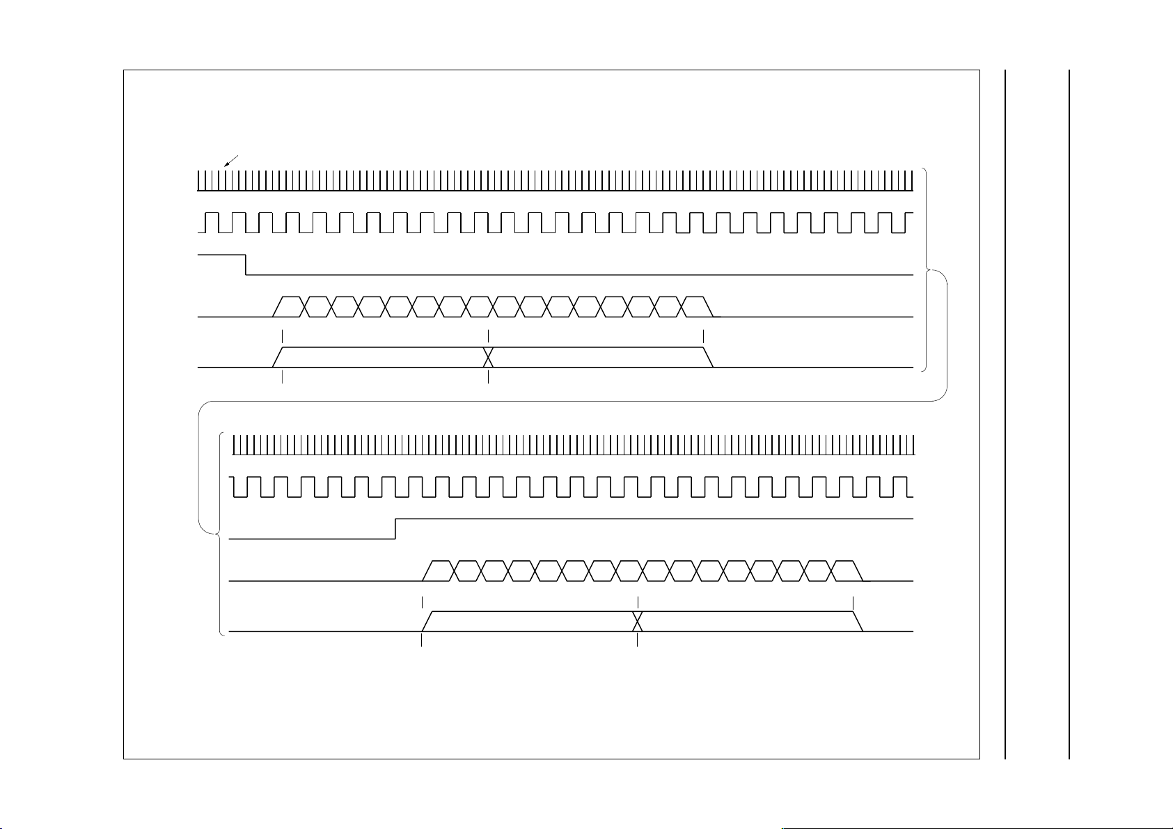
LTEN
transfer of 3 status bytes to microcontroller
Philips Semiconductors Product specification
Tape formatting and error
correction for the DCC system
LTCNT0,1
LTCLK
LTDATA
LTEN
LTCNT0,1
LTCLK
LTDATA
LTEN
LTCNT0,1
LTCLK
LTDATA
3HEX
t
d3
0 1 2 3 4 5 6 07 1 2 3 4 5 6 07 1 2 3 4 5 6 7
transfer of 2 SYSINFO bytes to microcontroller (in fast transfer period)
2HEX
0 1 2 3 4 5 6 7
10010000
transfer of 2 SYSINFO bytes from microcontroller (in fast transfer period)
2HEX
0 1 2 3 4 5 6 7
11010000
1HEX
t
ds1
0 1 2 3 4 5 6 07 1 2 3 4 5 6 7
0HEX
t
dr1
0 1 2 3 4 5 6
t
d3
status byte 2status byte 1status byte 0
t
ds2
t
dr2
07
1 2 3 4 5 6
second SYSINFO bytefirst SYSINFO bytecommand WRSYS
second SYSINFO bytefirst SYSINFO bytecommand RDSYS
7
MEA712 - 1
SAA2022
Fig.17 LT interface timing (2).
Page 27

February 1994 27
LTEN
transfer of two SYSINFO bytes starting at byte # 8 to microcontroller (in fast transfer period)
Philips Semiconductors Product specification
Tape formatting and error
correction for the DCC system
LTCNT0,1
LTCLK
LTDATA
LTEN
LTCNT0,1
LTCLK
LTDATA
2HEX 0HEX 2HEX
Idbyte 08hex rdsys sysinfo (8) sysinfo (9)
transfer of two SYSINFO bytes starting at byte # 8 from microcontroller to SAA2022 (in fast transfer period)
2HEX
0HEX
Idbyte 08hex wrsys
2HEX
0HEX
1HEX
0HEX
sysinfo (8) sysinfo (9)
1HEX
MEA714
SAA2022
Fig.18 LT interface timing (3).
Page 28

February 1994 28
Philips Semiconductors Product specification
Tape formatting and error
correction for the DCC system
LTEN
LTCNT0,1
LTCLK
LTDATA
LTEN
LTCNT0,1
LTCLK
LTDATA
transfer of two scratch pad RAM bytes (SPR) starting at SPR page 3, column 5, row 23 to microcomputer
2HEX 0HEX 2HEX 0HEX 2HEX 1HEX 1HEX
Idbyte 97hex
transfer of two scratch pad RAM bytes (SPR) starting at SPR page 3, column 5, row 23 from microcontroller to SAA2022
2HEX 0HEX 2HEX 0HEX 2HEX
Idbyte 97hex 38hex wrdrac
L
draccnt
L
draccnt
(in fast transfer period)
38hex rddrac spr (3,5,23) spr (3,5,24)
(in fast transfer period)
0HEX 0HEX
spr (3,5,23) spr (3,5,24)
MEA713
Fig.19 LT interface timing (4).
SAA2022
Page 29

Philips Semiconductors Product specification
Tape formatting and error
correction for the DCC system
100 %
91 %
duty
factor
speed
50 %
9 %
0
+ 2 blocks
+ 10.6 ms
+ 1.65 blocks
+ 8.8 ms
SAA2022
MEA717
0
– 1.65 blocks
– 8.8 ms
– 2 blocks
– 10.6 ms
SNUM
AUXBLK
AUX CHN
RECLAB
SYSBLK
DATA CHN
Fig.20 SPEED pulse width as a function of phase error.
01 23 0123012301
23012301230123
012320 0123012301230 2
012301230123012301230123
23
01
01230123
23012301
MEA706
Fig.21 Recording a label.
February 1994 29
Page 30

Philips Semiconductors Product specification
Tape formatting and error
correction for the DCC system
Table 4 Microcontroller Interface Commands.
CMD
REGISTER
76543210
XXXX1000 RDAUX read AUXILIARY INFO
XXXX1001 RDSYS read SYSINFO
XXXX1010 WRAUX write AUXILIARY INFO
XXXX1011 WRSYS write SYSINFO
XXXX0000 LDSET0 load new settings register 0
XXXX0001 LDSET1 load new settings register 1
XXXX0010 LDAFLEV load AUX flag threshold level
XXXX0011 LDSPDDTY load record speed duty cycle
XXXX0101 LDBYTCNT load byte counter
XXXX0110 LDRACCNT load random access counter
COMMAND EXPLANATION
SAA2022
XXYZ1100 RDDRAC read data in random access mode from RAM quarter YZ
XXYZ1101 RDFDRAC read flag and data in random access mode from RAM quarter YZ
XXYZ1110 WRDRAC write data in random access mode to RAM quarter YZ
XXYZ1111 WRFDRAC write flag and data in random access mode to RAM quarter YZ
Explanation of settings
SET0 R
µ
An active HIGH, selects microprocessor control for the
SPEED pulse width modulated servo control signal.
EGISTER (TABLE 6)
CSPD
DISRSY
Disable Resyncs active HIGH, is used in after recording.
RECLAB
Record labels active HIGH when in DRAR or DPAR
modes; a label being defined as the bodies of all four AUX
tape blocks in a tape frame which is being written.
This setting has immediate effect and should only be
modified in time segment 1.
ENFREG
In modes DPAP and DPAR Enable Frequency Regulation
active HIGH, allows frequency information from the data
channels to be used with the phase information to
generate the capstan SPEED signal.
ENEFREG
Enable Extended Frequency Regulation active HIGH,
allows extended frequency information from the data
channels to be used with the “normal” frequency
information and the phase information to generate the
capstan SPEED signal, if ENFREG is active.
SET1 R
EGISTER (TABLE 7)
TEST1
This setting is for test only. For use in applications this bit
should be always programmed to logic 0.
PINO1
Pin Output 1, Port expander output for the microcontroller.
TFEMAS
This allows the SAA2022 to become master of the
SB-I2S-bus in modes DPAP and DPAR. In mode DRAR
the device always operates as a slave irrespective of the
settings bit.
February 1994 30
Page 31

Philips Semiconductors Product specification
Tape formatting and error
correction for the DCC system
PORTAB
Portable application active HIGH, allows for the data
channels clock extraction to track fast variations in tape bit
rate. For home use set to inactive.
NOCOS
No Corrected Output Symbol active HIGH, disables the
writing of the error corrected output to the DRAM. It is only
used for debugging.
TEST2
This setting is for test only. For use in applications this bit
should always be programmed to logic 0.
PINO2
Pin output 2, Port expander output for the microcontroller.
PINO3
Pin output 3, Port expander output for the microcontroller.
APE PHASE MODE
T
SAA2022
E
XTENDED TAPE FREQUENCY MODE
ENFREG = logic 1, ENEFREG = logic 1 and
µ
CSPD = logic 0
In this mode there are 3 regions. This provides a more
gentle transition from frequency plus phase control to
phase only control. Firstly from 0% to ±4.5% deviation,
where the operation is as for the tape phase mode.
Secondly from ±4.5% to ±6% deviation where the
contribution of the frequency information to the servo
information is half of that in the region beyond ±6%
deviation. Thirdly when the deviation is greater than ±6%,
which is the same as for the tape frequency mode.
ICROCONTROLLER MODE
M
µ
CSPD = logic 1
In this mode the pulse width is determined by the
microcontroller programming of the SPDDTY interface
register.
NMODE0, NMODE1
ENFREG = logic 0, ENEFREG = logic 0 and
µ
CSPD = logic 0
In this mode the SAA2022 performs a new calculation to
determine the pulse width for the SPEED signal
approximately once every 21.33 ms, giving a sampling
rate of approximately 46.9 Hz. This calculation is basically
a phase comparison between the incoming main data tape
frame and an internally generated reference. The pulse
duty cycle increases linearly from approximately 9% when
the incoming main data tape frame is 1.65 tape blocks
(8.8 ms) too early up to 91% when the incoming main data
tape frame is 1.65 tape blocks (8.8 ms) too late, in 256
steps (see Fig.20). Outside ±2 tape blocks range the pulse
width characteristic overflows and repeats itself forming a
saw-tooth pattern. The SAA2022 has an internal buffer of
±8.8 ms inside which the phase information is valid.
T
APE FREQUENCY MODE
ENFREG = logic 1, ENEFREG = logic 0 and
µ
CSPD = logic 0
The above description is overridden with frequency
information. That is if the incoming main data bit rate
deviates by more than approximately ±6% from the
nominal bit rate of 96000 bits per second, frequency
information is mixed with the phase information. In
between the limits ±6% the pulse width is determined as
above.
These two bits control the mode change operation in the
SAA2022.
Table 5 NMODE1, NMODE0.
NMODE1 NMODE0 OPERATING MODE
0 0 DPAP
1 0 DPAR
1 1 DRAR
0 1 invalid state
February 1994 31
Page 32

Philips Semiconductors Product specification
Tape formatting and error
correction for the DCC system
SETTINGS REGISTERS
Table 6 SET0.
SETTING BIT DEFAULT
ENEFREG 6 0
ENFREG 5 0
RECLAB 4 0
DISRSY 3 0
µCSPD 2 0
NMODE1 1 0
NMODE0 0 0
Table 7 SET1.
SETTING BIT DEFAULT
PINO3 7 0
PINO2 6 0
SAA2022
Table 8 SPEED Source.
MODE µCSPD SPEED
DPAP 0 tape
DPAP 1 µC
DPAR 0 tape
DPAR 1 µC
DRAR 0 50%
DRAR 1 µC
Notes
1. “Tape” means that the duty cycle has been calculated
from the playback tape signal.
2. “µC” means that the microcontroller programs the
duty cycle via the SPDDTY register in the
microcontroller interface.
3. “50%” defines that the duty cycle is fixed at 50%.
(1)
(2)
(1)
(2)
(3)
(2)
TEST2 5 0
NOCOS 4 0
PORTAB 3 1
TFEMAS 2 1
PINO1 1 0
TEST1 0 0
Table 9 Typical Settings.
SETTING BYTE
WHEN01
7654321076543210
X 1 1 0 0 0 0 0 0 0 0 0 0 1 0 0 play home machine
X 1 1 0 0 0 0 0 0 0 0 0 1 1 0 0 play portable machine
X X X 0 X 0 1 1 0 0 0 0 0 1 0 0 record NO LABEL
X X X 1 X 0 1 1 0 0 0 0 0 1 0 0 record LABEL
X X X 0 1 1 1 0 0 0 0 0 0 1 0 0 after record NO LABEL
X X X 1 1 1 1 0 0 0 0 0 0 1 0 0 after record LABEL
February 1994 32
Page 33

Philips Semiconductors Product specification
Tape formatting and error
SAA2022
correction for the DCC system
STATUS REGISTERS
The SAA2022 has 4 status registers all of which are read only. A circular pointer is used to select which of the status
registers is addressed. This pointer is reset to point to STATUS0 as result of the rising edge of LTEN while the LTCNT0/
1 = RSTAT. Any number of the registers may be read, always starting at STATUS0.
Table 10 STATUS0.
STATUS BIT BIT
RFBT 7
SYSFLC 6
AUXFLC 5
AUXFLO 4
FLAGI 3
URDA 2
SNUM1 1
Table 12 STATUS2.
STATUS BIT BIT
NFLG3 7
NFLG2 6
NFLG1 5
NFLG0 4
FLG3 3
FLG2 2
FLG1 1
SNUM0 0
Table 11 STATUS1.
STATUS BIT BIT
SLOWTFR 7
TEST4 6
− 5
PINI 4
PAG2 3
PAG1 2
MODE1 1
MODE0 0
FLG0 0
Table 13 STATUS3.
STATUS BIT BIT
CHANS7 7
CHANS6 6
CHANS5 5
CHANS4 4
CHANS3 3
CHANS2 2
CHANS1 1
CHANS0 0
February 1994 33
Page 34

Philips Semiconductors Product specification
Tape formatting and error
correction for the DCC system
SNUM0, SNUM1
Time segment number.
URDA
Unreliable Data active HIGH, means that regardless of the
other flag information you cannot use the Data,
SYSINFO or AUX, because they are unreliable, this can
occur as result of a RESYNC, a mode change from mode
DRAR to mode DPAP, or a reset of the SAA2022. When a
resync occurs it resynchronizes with the incoming main
data tape channel information, with a result that for a
period of time, the time that URDA is HIGH all output data
is unusable.
FLAGI
Instantaneous flag active HIGH, indicates that the
AUXILIARY byte that is about to be transferred to the
microcontroller has a flag that is ≥ AFLEV, or that the
SYSINFO byte that is about to be transferred is in error.
AUXFLO
Old Aux Flag active HIGH, indicates that AUXILIARY data
due to be transferred to the microcontroller in the current
segment should not be used.
AUXFLC
AUX Flag active HIGH, indicates that at least one of the
AUXILIARY data bytes due to be transferred to the
microcontroller in the current segment is in error. This
information is provided before the transfer occurs.
SYSFLC
SYSINFO flag active HIGH, indicates that at least one of
the SYSINFO bytes in the current segment is in error. This
information is provided before the transfer occurs.
RFBT
Ready for byte transfer of SYSINFO, AUX or Scratch pad
RAM to or from the microcontroller active HIGH.
SAA2022
PINI
Pin input, Port expander input for the microcontroller.
TEST4
This is for test purposes only.
SLOWTFR
Indicates that LT data transfers of SYSINFO, AUX or
Scratch Pad RAM can only occur at low speed rate. This
occurs only during the second half of time segment 0,
therefore the status bit RFBT must be polled to see if a
transfer is possible. This bit will be HIGH only during the
second half of time segment 0.
FLG 0 to 3
Error flag from the next AUXILIARY/SYSINFO byte which
is to be transferred to the microcontroller.
The flags for SYSINFO bytes have only 2 values, logic 0
which implies that the error corrector finds the bytes are
good and logic 1 which implies that the bytes are in error.
The flags for AUXINFO bytes can have any one of 16
values, 0 to 15, depending on the type of correction. All of
the AUX bytes in the same AUX code word will have the
same flag value. The less reliable the data, the higher the
flag value. It is recommended that any byte with a flag
value of 10 or higher is deemed unreliable.
NFLG 0 to 3
Error flag from the byte after the next AUXILIARY/
SYSINFO byte which will be transferred to the
microcontroller.
CHANS 0 to 7
Error Correction Channel status, which indicates if the
even C1 code words in the 5th block of the segment for
each data tape channel were non correctable. Therefore 1
in every 16 C1 code words from each channel is monitored
to see if the C1 error correcting decoding was successful.
MODE0, MODE1
Current mode of operation of the SAA2022.
PAG1, PAG2
Two most significant bits of the modulo 6 internal page
counter, the least significant bit is equal to SNUM0.
February 1994 34
Page 35

Philips Semiconductors Product specification
Tape formatting and error
SAA2022
correction for the DCC system
Loadable registers
Table 14 AFLev.
3210 BIT
1 0 1 0 default value
AUX Flag threshold level. FLAGI goes HIGH for the AUX bytes whose flags are ≥ AFLev. AUXFLC will go HIGH if the
flags from either code word in the current segment are ≥ AFLev. The default value is 10.
Table 15 SPDDTY.
76543210 BIT
10000000default value
SPEED duty cycle register. If µCSPD is active, this register determines the duty cycle of the speed signal.
The duty cycle is given by:
Duty cycle
SPDDTY 100
------------------------------------------=
256
×
%
• 0 for 0% duty cycle
• 128 for 50% duty cycle
• 255 for 99.6% duty cycle.
The default value is 128.
Table 16 BYTCNT.
76543210 BIT
00000000default value
Byte counter for SYSINFO, AUX and Scratch Pad RAM
transfers. For SYSINFO:
values 0 to 31 access SYSINFO from the current segment.
values 32 to 63 access SYSINFO from the current +1 segment.
values 64 to 95 access SYSINFO from the current +2 segments.
values 96 to 127 access SYSINFO from the current +3 segments.
In Random access mode the SYSTEM ADDRESS is mapped on to BYTCNT as follows:
Table 17 SYSTEM ADDRES in Random access mode.
76543210 BYTCNT
76543210ROW
Table 18 RAACNT.
6543210 BIT
0000000default value
February 1994 35
Page 36

Philips Semiconductors Product specification
Tape formatting and error
SAA2022
correction for the DCC system
Random Access counter is used for generating addresses in the Random access mode, the SYSTEM ADDRESS is
mapped on to RACCNT as shown in Table 19.
Table 19 SYSTEM address.
6543210 RACCNT
−−−−−−8 ROW
−−−210−COL
210−−−−PAG
SYSINFO AND AUX DATA OFFSETS
AUX data consists of 4 blocks of 36 bytes, one block being
transferred in each time segment.
Each tape frame contains 128 bytes of SYSINFO, the
SYSINFO bytes can for convenience, be considered as
being grouped into 4 SYSINFO blocks, with:
SYSBlk0 ==> SI0 to SI31,
SYSBlk1 ==> SI32 to SI63, etc.
In modes DPAP and DPAR SYSINFO transfers may occur
in two ways:
1. 4 blocks of 32 bytes, one block being transferred from
the SAA2022 in each time segment.
2. 1 block of 128 bytes being transferred in time
segment 1.
In mode DRAR SYSINFO must be transferred to the
SAA2022 as 4 blocks of 32 bytes, one block in each
segment.
Figures 26 to 29 show the offsets between the SYSINFO
and AUX and the time segment counter, for the various
modes of operation of the SAA2022.
February 1994 36
Page 37

Philips Semiconductors Product specification
Tape formatting and error
correction for the DCC system
BLOCK OFFSETS WITH RESPECT TO TIME SEGMENT
Mode DPAP
SYSBlk = (SNUM + 3) MOD 4;
or read all 4 SYSINFO blocks when SNUM = 1.
If AUX and MAIN were recorded simultaneously then
AUXBlk = (SNUM + 1) MOD 4; else read and interpret
1 AUX block in each time segment.
Mode DRAR
SYSBlk = SNUM;
AUXBlk = (SNUM + 1) MOD 4.
Mode DPAR
SYSBlk = (SNUM + 3) MOD 4;
or read all 4 SYSINFO blocks when SNUM = 1;
AUXBlk = (SNUM + 1) MOD 4.
T
HE SCRATCH PAD RAM
The SAA2022 provides the microcontroller with a scratch
pad RAM, which it can use for any purpose. The size of the
scratch pad depends upon the size of the DRAM used and
the locations may be written and read in 8-bit or 12-bit
units.
For a 64 k × 4-bit DRAM, the scratch pad is arranged as
6 pages, where each page consists of
7 columns × 64 rows. The pages are numbered 0 to 5,
columns 1 to 7 and rows 0 to 63. This gives a total of
(6 × 7 × 64) = 2688 locations.
For a 256 k × 4-bit DRAM, the scratch pad is the same as
for the 64 k × 4 bit DRAM, plus an additional 3 RAM
SAA2022
quarters, each of 6 pages where each page consists of
8 columns × 448 rows. The pages are numbered 0 to 5,
columns 0 to 7 and rows 0 to 431. This gives then a total
of (2688 + (3 × 6 × 8 × 448)) = 67200 locations. The RAM
quarter is chosen by the YZ bits of the microcontroller
interface commands.
Use of the scratch pad RAM outside the above ranges will
upset the operation of the device.
As with SYSINFO, AUX transfers can occur at high-speed
at all times except the second half of time segment 0, that
is when the status bit SLOWTFR is HIGH. During this
period the microcontroller must poll the status bit RFBT to
determine when a transfer can occur.
There are two possible methods for addressing the scratch
pad RAM. For random access of the scratch pad the
address of each location is sent by the microcontroller to
the SAA2022 before each location transfer. Alternatively,
the address of the first location can be sent by the
microcontroller before the first location transfer. This will
automatically increment the row for all subsequent
transfers until the end of the column. The RACCNT and
BYTCNT registers are used for addressing the scratch
pad. For the 64 k × 4-bit DRAM, and first quarter of
256 k × 4 DRAM the mapping of the scratch pad RAM
address onto the RACCNT and BYTCNT registers is
shown in Tables 20 and 21. For the other three-quarters of
the 256 k × 4 DRAM the mapping of the scratch pad RAM
address onto the RACCNT and BYTCNT registers is
shown in Tables 22 and 23.
Table 20 RACCNT bit.
RACCNT BIT
6543210
P2 P1 P0 C2 C1 C0 1
Table 21 BYTCNT bit.
BYTCNT BIT
76543210
1 0 R5 R4 R3 R2 R1 R0
February 1994 37
Table 22 RACCNT bit.
RACCNT BIT
6543210
P2 P1 P0 C2 C1 C0 R8
Table 23 BYTCNT bit.
BYTCNT BIT
76543210
R7 R6 R5 R4 R3 R2 R1 R0
Page 38

Philips Semiconductors Product specification
Tape formatting and error
correction for the DCC system
Mode changes
Table 24 Possible mode changes for the SAA2022.
CURRENT MODE
DPAP DRAR DPAR
DPAP − YES YES
DRAR YES −−
DPAR YES −−
TIMING FOR MODE CHANGES
Mode change DPAP to DRAR
This mode change occurs at the end of the time segment
in which the SAA2022 receives the new settings. Writing
of the first MAIN and AUX data commences at the start of
the time segment 1 which follows two subsequent end of
time segment 3 intervals. The delay to writing to tape is
approximately 222 ms, as shown in Fig.22. If “seamless
appending” is required the new settings should be sent to
the SAA2022 during time segment 2.
Mode change DPAP to DPAR
This mode change occurs at the first end of time segment
2 after the SAA2022 receives the new settings. Output of
AUX to tape begins at the start of the following time
segment 1, (i.e. ≈85.3 ms after the mode change), as
shown in Fig.23.
SAA2022
NEW MODE
Mode change DRAR to DPAP
This mode change occurs at the first end of time
segment 0 after the SAA2022 receives the new setting.
Writing of MAIN and AUX data stops immediately after the
mode change. The time segment jumps back to 0, URDA
goes HIGH and stays HIGH for 5 time segments
(≈213.3 ms) after which it goes LOW, as shown in Fig.24.
Mode change DPAR to DPAP
This mode change occurs at the first end of time
segment 0 after the SAA2022 receives the new setting.
The writing of AUX data to tape stops immediately after the
mode change. The first AUX read from tape can be
expected during the following time segment 0 or 1 (i.e.
128 to 170.67 ms after the mode change), as shown in
Fig.25.
February 1994 38
Page 39

Philips Semiconductors Product specification
Tape formatting and error
correction for the DCC system
handbook, halfpage
AUXILIARY, MAIN
NEW MODE
TAPE OUT
SNUM
MODE
01 230123012
DPAP DRAR
DRAR
≈
222 ms
MEA707 - 2
handbook, halfpage
SNUM
MODE
NEW MODE
AUXILIARY
TAPE OUT
SAA2022
1230123012
DPAP
≈
85.3 ms
DPAR
DPAR
MEA708 - 2
Fig.22 Mode change DPAP to DRAR (AUX
and MAIN simultaneously recording).
handbook, halfpage
SNUM
MODE
NEW MODE
URDA
1230 12301
DRAR
DPAP
0
DPAP
≈
213.3 ms
MEA709 - 1
Fig.23 Mode change DPAP to DPAR
handbook, halfpage
NEW MODE
AUXILIARY
TAPE OUT
AUXILIARY
MICROCONTROLLER
(AUX after recording).
SNUM
MODE
1230123012
DPAR DPAP
DPAP
≈
128 ms
TO
≈
170.66 ms
MEA710 - 2
Fig.24 Mode change DRAR to DPAP.
February 1994 39
Fig.25 Mode change DPAR to DPAP.
Page 40

Philips Semiconductors Product specification
Tape formatting and error
correction for the DCC system
SNUM
AUX BLK
SYS BLK
SYS BLK
AUX, MAIN
DATA INPUT
FROM TAPE
01 23 0123012
123012301230123
3012301230122301
*
0
1
2
3
01 23 01230123012
0
1
2
3
0
1
2
3
SAA2022
3012
0
1
2
3
MLB413
Fig.26 SYSINFO and AUX block delays in DPAP (Audio and AUX simultaneously recorded).
SNUM
AUX BLK
SYS BLK
SYS BLK
AUX, MAIN
DATA INPUT
FROM TAPE
01 23 0123012
DEPENDS ON PHASE OF AUX WRT MAIN DATA CHANNELS
3012301230122301
*
0
1
2
3
01 23 01230123012
0
1
2
3
0
1
2
3
3012
0
1
2
3
MLB414
Fig.27 SYSINFO and AUX block delays in mode DPAP (Audio and AUX recorded separately).
February 1994 40
Page 41

Philips Semiconductors Product specification
,
,
,
,
,
Tape formatting and error
correction for the DCC system
SNUM
AUX BLK
SYS BLK
AUX, MAIN
DATA OUTPUT
FROM TAPE
01 23 0123012
123012301230123
01 23 01230123012
3012301230122301
SAA2022
3012
MLB415
Fig.28 SYSINFO and AUX block delays in mode DRAR.
SNUM
AUX BLK
SYS BLK
SYS BLK
MAIN DATA
INPUT
FROM TAPE
AUX OUTPUT
TO TAPE
01 23 0123012
123012301230123
,,,
3012301230122301
*
0
1
2
,
3
0
1
2
3
,
0
1
2
3
,
01 23 01230123012
012301230122301
1
,,,,
3012
0
1
2
3
MLB416
Fig.29 SYSINFO and AUX block delays in mode DPAR.
February 1994 41
Page 42

Philips Semiconductors Product specification
Tape formatting and error
SAA2022
correction for the DCC system
LIMITING VALUES
In accordance with the Absolute Maximum Rating System (IEC 134).
SYMBOL PARAMETER CONDITIONS MIN. MAX. UNIT
V
DD
V
I
I
SS
I
DD
I
I
I
O
P
tot
T
stg
T
amb
V
es1
V
es2
supply voltage −0.5 +6.5 V
input voltage note 1 −0.5 VDD + 0.5 V
supply current in V
supply current in V
SS
DD
−−100 mA
− 100 mA
input current −10 +10 mA
output current −20 +20 mA
total power dissipation − 500 mW
storage temperature −55 +150 °C
operating ambient temperature −40 +85 °C
electrostatic handling note 2 −1500 +1500 V
electrostatic handling note 3 −70 +70 V
Notes
1. Input voltage should not exceed 6.5 V unless otherwise specified.
2. Equivalent to discharging a 100 pF capacitor through a 1.5 kΩ series resistor.
3. Equivalent to discharging a 200 pF capacitor through a 0 Ω series resistor.
DC CHARACTERISTICS
= 3.8 to 5.5 V; T
V
DD
= −40 to +85 °C; unless otherwise specified.
amb
SYMBOL PARAMETER CONDITIONS MIN. TYP. MAX. UNIT
Supply
V
DD
I
DD
supply voltage note 1 3.8 5.0 5.5 V
supply current VDD= 5 V − 21 30 mA
= 3.8 V − 16 25 mA
V
DD
Inputs CLK24, TCH0 to TCH7, TAUX, PWRDWN, LTCLK, LTCNT0, LTCNT1, LTEN, PINI and SBMCLK
V
IL
V
IH
I
I
LOW level input voltage −−0.3V
HIGH level input voltage 0.7V
input current VI = 0 V; T
= 5.5 V; T
V
I
= 25 °C −−−10 µA
amb
= 25 °C −−10 µA
amb
−−V
DD
DD
V
February 1994 42
Page 43

Philips Semiconductors Product specification
Tape formatting and error
SAA2022
correction for the DCC system
SYMBOL PARAMETER CONDITIONS MIN. TYP. MAX. UNIT
Input RESET
V
tLH
threshold voltage
LOW-HIGH
V
tHL
threshold voltage
HIGH-LOW
V
hys
I
I
hysteresis V
input current VI = V
tLH
− V
tHL
DD
Outputs RASN, CASN, WCLOCK and WDATA
V
OL
V
OH
LOW level output voltage IO = −3mA −−0.4 V
HIGH level output voltage IO = 3 mA VDD − 0.5 −−V
Outputs LTREF, WEN, OEN, A0 to A8, SPEED, SPDF, PINO1, PINO3, AZCHK, TEST2, TEST3, MCLK, SBEF,
SBDIR and URDA
V
OL
V
OH
LOW level output voltage IO = −2mA −−0.4 V
HIGH level output voltage IO = 2 mA VDD − 0.5 −−V
Inputs/outputs D0 to D3; with outputs in 3-state
0.8V
−−0.2V
−−V
DD
DD
V
− 1.5 − V
25 − 400 µA
V
IL
V
IH
I
I
LOW level input voltage TTL-level −−0.8 V
HIGH level input voltage TTL-level 2 −−V
input leakage current VI = 0 V; T
= 5.5 V; T
V
I
= 25 °C −−−10 µA
amb
= 25 °C −−10 µA
amb
Inputs/outputs D0 to D3
V
OL
V
OH
LOW level output voltage IO = −3mA −−0.4 V
HIGH level output voltage IO = 3 mA VDD − 0.5 −−V
Inputs/outputs LTDATA, SBCL, SBDA and SBWS; with outputs in 3-state
V
IL
V
IH
I
I
LOW level input voltage TTL-level −−0.3V
HIGH level input voltage TTL-level 0.7V
input leakage current VI = 0 V; T
= 5.5 V; T
V
I
= 25 °C −−−10 µA
amb
= 25 °C −−10 µA
amb
Inputs/outputs LTDATA, SBCL, SBDA and SBWS
V
OL
V
OH
LOW level output voltage IO = − 3mA −−0.4 V
HIGH level output voltage IO = 3 mA VDD − 0.5 −−V
Note
DD
−−V
DD
V
1. For applications requiring minimum power dissipation the device may be operated from a nominal +4 V supply.
February 1994 43
Page 44

Philips Semiconductors Product specification
Tape formatting and error
SAA2022
correction for the DCC system
AC CHARACTERISTICS
= 3.8 to 5.5 V; T
V
DD
SYMBOL PARAMETER CONDITIONS MIN. TYP. MAX. UNIT
Clock inputs
C
i
input capacitance −−10 pF
CLK24
f pulse frequency 23 24.576 26 MHz
t
L-i
t
H-i
pulse width LOW 10 −−ns
pulse width HIGH 10 −−ns
SBMCLK
f pulse frequency − 6.144 12.5 MHz
t
L-i
t
H-i
pulse width LOW 30 −−ns
pulse width HIGH 30 −−ns
Clock outputs
= −40 to +85 °C; unless otherwise specified.
amb
C
L
load capacitance −−50 pF
MCLK
f pulse frequency − 6.144 − MHz
t
L-i
t
H-i
t
dMFR
t
d
pulse width LOW 50 −−ns
pulse width HIGH 50 −−ns
delay time from CLK24 note 1 −−45 ns
delay time from PWRDWN − 15 − ns
Clock inputs
C
i
input capacitance −−10 pF
Inputs LTCLK, LTCNT0, LTCNT1, LTEN, RESET, TCH0 to TCH7 and TAUX
t
suMR
t
hMR
set-up time to MCLK note 2 40 −−ns
hold time from MCLK note 2 0 −−ns
Input PINI
t
suMR
t
hMR
set-up time to MCLK note 1 70 −−ns
hold time from MCLK note 1 0 −−ns
Outputs
C
L
load capacitance −−50 pF
February 1994 44
Page 45

Philips Semiconductors Product specification
Tape formatting and error
SAA2022
correction for the DCC system
SYMBOL PARAMETER CONDITIONS MIN. TYP. MAX. UNIT
Outputs A0 to A8, AZCHK, TEST2, LTREF, SBDIR, SBEF, SPDF, SPEED, PINO1 to PINO3, URDA, WCLOCK,
WDATA, OEN and WEN
t
dMR
Outputs OEN and WEN
t
d
Output RASN
t
dFR
t
d
Output CASN
t
dFR
t
d
Inputs/outputs
C
i
C
L
Inputs/outputs D0 to D3
delay time from MCLK note 2 −−30 ns
delay time from PWRDWN − 15 − ns
delay time from CLK24 note 1 −−30 ns
delay time from PWRDWN − 15 − ns
delay time from CLK24 note 1 −−30 ns
delay time from PWRDWN − 15 − ns
input capacitance −−10 pF
load capacitance −−50 pF
t
suCR
t
hCR
t
dMR
t
d
set-up time to CASN note 3 10 −−ns
hold time from CASN note 3 0 −−ns
delay time from MCLK note 2 −−25 ns
delay time from PWRDWN − 15 − ns
Input/output LTDATA
t
suMR
t
hMR
t
dMR
t
d
t
d
set-up time to MCLK note 2 40 −−ns
hold time from MCLK note 2 0 −−ns
delay time from MCLK note 2 −−30 ns
delay time from PWRDWN − 15 − ns
delay time from LTEN − 15 − ns
Inputs/outputs SBCL and SBWS
t
suMR
t
hMR
t
dSR
t
dMR
t
d
set-up time to MCLK note 2 40 −−ns
hold time from MCLK note 2 0 −−ns
delay time from SBMCLK note 3 −−40 ns
delay time from MCLK notes 2 and 5 −−30 ns
delay time from PWRDWN − 15 − ns
February 1994 45
Page 46

Philips Semiconductors Product specification
Tape formatting and error
SAA2022
correction for the DCC system
SYMBOL PARAMETER CONDITIONS MIN. TYP. MAX. UNIT
Input/output SBDA
t
suMR
t
hMR
t
dMR
t
d
Notes
1. LOW-to-HIGH transition of CLK24.
2. LOW-to-HIGH transition of MCLK.
3. LOW-to-HIGH transition of CASN.
4. LOW-to-HIGH transition of SBMCLK.
5. 3-state control.
set-up time to MCLK note 2 40 −−ns
hold time from MCLK note 2 0 −−ns
delay time from MCLK note 2 −−30 ns
delay time from PWRDWN − 15 − ns
CLK24
OUT1
MCLK
IN1
OUT2
CASN
IN2
SBMCLK
OUT3
t
dMFR
t
dFR
t
suCR
t
L– i
t
suMR
t
hCR
t
dFR
t
dFR
t
t
dSR
hMR
t
t
H– i
t
L–i
t
dMR
H–O
t
H–i
t
L–O
t
dMFR
MEA716 - 1
Fig.30 Timing for AC characteristics.
February 1994 46
Page 47

Philips Semiconductors Product specification
Tape formatting and error
correction for the DCC system
PACKAGE OUTLINE
seating plane
64 52
1
pin 1 index
0.15
19.2
18.2
SAA2022
S
S
B
51
1.2
(4x)
0.8
1.0
20.1
19.9
25.2
24.2
1.55
0.85
X
1.45
1.15
0.25
0.14
o
0 to 7
MBC658 - 1
3.2
2.7
B
0.15 M
0.50
0.35
3220
0.30
0.05
33
1.2
(4x)
0.8
A
detail X
19
1.0
0.50
0.35
14.1
13.9
0.15 M A
2.85
2.65
Dimensions in mm.
Fig.31 64-lead quad flat-pack; plastic (SOT208).
February 1994 47
Page 48

Philips Semiconductors Product specification
Tape formatting and error
correction for the DCC system
SOLDERING
Quad flat-packs
B
YWAVE
During placement and before soldering, the component
must be fixed with a droplet of adhesive. After curing the
adhesive, the component can be soldered. The adhesive
can be applied by screen printing, pin transfer or syringe
dispensing.
Maximum permissible solder temperature is 260 °C, and
maximum duration of package immersion in solder bath is
10 s, if allowed to cool to less than 150 °C within 6 s.
Typical dwell time is 4 s at 250 °C.
A modified wave soldering technique is recommended
using two waves (dual-wave), in which, in a turbulent wave
with high upward pressure is followed by a smooth laminar
wave. Using a mildly-activated flux eliminates the need for
removal of corrosive residues in most applications.
B
Y SOLDER PASTE REFLOW
Reflow soldering requires the solder paste (a suspension
of fine solder particles, flux and binding agent) to be
applied to the substrate by screen printing, stencilling or
pressure-syringe dispensing before device placement.
SAA2022
Several techniques exist for reflowing; for example,
thermal conduction by heated belt, infrared, and
vapour-phase reflow. Dwell times vary between 50 and
300 s according to method. Typical reflow temperatures
range from 215 to 250 °C.
Preheating is necessary to dry the paste and evaporate
the binding agent. Preheating duration: 45 min at 45 °C.
EPAIRING SOLDERED JOINTS (BY HAND-HELD SOLDERING
R
IRON OR PULSE-HEATED SOLDER TOOL
Fix the component by first soldering two, diagonally
opposite, end pins. Apply the heating tool to the flat part of
the pin only. Contact time must be limited to 10 s at up to
300 °C. When using proper tools, all other pins can be
soldered in one operation within 2 to 5 s at between 270
and 320 °C. (Pulse-heated soldering is not recommended
for SO packages.)
For pulse-heated solder tool (resistance) soldering of VSO
packages, solder is applied to the substrate by dipping or
by an extra thick tin/lead plating before package
placement.
)
February 1994 48
Page 49

Philips Semiconductors Product specification
Tape formatting and error
SAA2022
correction for the DCC system
DEFINITIONS
Data sheet status
Objective specification This data sheet contains target or goal specifications for product development.
Preliminary specification This data sheet contains preliminary data; supplementary data may be published later.
Product specification This data sheet contains final product specifications.
Limiting values
Limiting values given are in accordance with the Absolute Maximum Rating System (IEC 134). Stress above one or
more of the limiting values may cause permanent damage to the device. These are stress rating only and operation of
the device at these or at any other conditions above those given in the Characteristics sections of the specification is
not implied. Exposure to limiting values for extended periods may affect device reliability.
Application information
Where application information is given, it is advisory and does not form part of the specification.
LIFE SUPPORT APPLICATIONS
These products are not designed for use in life support appliances, devices, or systems where malfunction of these
products can reasonably be expected to result in personal injury. Philips customers using or selling these products for
use in such applications do so at their own risk and agree to fully indemnify Philips for any damages resulting from such
improper use or sale.
The Digital Compact Cassette logo is a registered trade mark of Philips Electronics N.V.
February 1994 49
Page 50

Philips Semiconductors Product specification
Tape formatting and error
correction for the DCC system
SAA2022
NOTES
February 1994 50
Page 51

Philips Semiconductors Product specification
Tape formatting and error
correction for the DCC system
SAA2022
NOTES
February 1994 51
Page 52

Philips Semiconductors – a worldwide company
Argentina: IEROD, Av. Juramento 1992 - 14.b, (1428)
BUENOS AIRES, Tel. (541)786 7633, Fax. (541)786 9367
Australia: 34 Waterloo Road, NORTH RYDE, NSW 2113,
Tel. (02)805 4455, Fax. (02)805 4466
Austria: Triester Str. 64, A-1101 WIEN, P.O. Box 213,
Tel. (01)60 101-1236, Fax. (01)60 101-1211
Belgium: Postbus 90050, 5600 PB EINDHOVEN, The Netherlands,
Tel. (31)40 783 749, Fax. (31)40 788 399
Brazil: Rua do Rocio 220 - 5
CEP: 04552-903-SÃO PAULO-SP, Brazil.
P.O. Box 7383 (01064-970).
Tel. (011)829-1166, Fax. (011)829-1849
Canada: INTEGRATED CIRCUITS:
Tel. (800)234-7381, Fax. (708)296-8556
DISCRETE SEMICONDUCTORS: 601 Milner Ave,
SCARBOROUGH, ONTARIO, M1B 1M8,
Tel. (0416)292 5161 ext. 2336, Fax. (0416)292 4477
Chile: Av. Santa Maria 0760, SANTIAGO,
Tel. (02)773 816, Fax. (02)777 6730
Colombia: Carrera 21 No. 56-17, BOGOTA, D.E., P.O. Box 77621,
Tel. (571)217 4609, Fax. (01)217 4549
Denmark: Prags Boulevard 80, PB 1919, DK-2300 COPENHAGEN S,
Tel. (032)88 2636, Fax. (031)57 1949
Finland: Sinikalliontie 3, FIN-02630 ESPOO,
Tel. (9)0-50261, Fax. (9)0-520971
France: 4 Rue du Port-aux-Vins, BP317,
92156 SURESNES Cedex,
Tel. (01)4099 6161, Fax. (01)4099 6427
Germany: P.O. Box 10 63 23, 20095 HAMBURG ,
Tel. (040)3296-0, Fax. (040)3296 213
Greece: No. 15, 25th March Street, GR 17778 TAVROS,
Tel. (01)4894 339/4894 911, Fax. (01)4814 240
Hong Kong: 15/F Philips Ind. Bldg., 24-28 Kung Yip St.,
KWAI CHUNG, Tel. (0)4245 121, Fax. (0)4806 960
India: PEICO ELECTRONICS & ELECTRICALS Ltd.,
Components Dept., Shivsagar Estate, Block 'A',
Dr. Annie Besant Rd., Worli, BOMBAY 400 018,
Tel. (022)4938 541, Fax. (022)4938 722
Indonesia: Philips House, Jalan H.R. Rasuna Said Kav. 3-4,
P.O. Box 4252, JAKARTA 12950,
Tel. (021)5201 122, Fax. (021)5205 189
Ireland: Newstead, Clonskeagh, DUBLIN 14,
Tel. (01)640 000, Fax. (01)640 200
Italy: Viale F. Testi, 327, 20162 MILANO,
Tel. (02)6752.1, Fax. (02)6752.3350
Japan: Philips Bldg13-37 , Kohnan 2-chome, Minato-ku, KOKIO 108,
Tel. (03)3740 5101, Fax. (03)3740 0570
Korea: (Republic of) Philips House, 260-199 Itaewon-dong,
Yongsan-ku, SEOUL, Tel. (02)794-5011, Fax. (02)798-8022
Malaysia: No. 76 Jalan Universiti, 46200 PETALING JAYA,
SELANGOR, Tel. (03)757 5511, Fax. (03)757 4880
Mexico: Philips Components, 5900 Gateway East, Suite 200,
EL PASO, TX 79905, Tel. 9-5(800)234-7381, Fax. (708)296-8556
Netherlands: Postbus 90050, 5600 PB EINDHOVEN,
Tel. (040)78 37 49, Fax. (040)78 83 99
New Zealand: 2 Wagener Place, C.P.O. Box 1041, AUCKLAND,
Tel. (09)849-4160, Fax. (09)849-7811
Norway: Box 1, Manglerud 0612, OSLO,
Tel. (22)74 8000, Fax. (22)74 8341
th
floor, Suite 51,
Pakistan: Philips Markaz, M.A. Jinnah Rd., KARACHI 3,
Tel. (021)577 039, Fax. (021)569 1832
Philippines: PHILIPS SEMICONDUCTORS PHILIPPINES Inc,
106 Valero St. Salcedo Village, P.O. Box 911, MAKATI,
Metro MANILA, Tel. (02)810 0161, Fax. (02)817 3474
Portugal: Av. Eng. Duarte Pacheco 6, 1009 LISBOA Codex,
Tel. (01)683 121, Fax. (01)658 013
Singapore: Lorong 1, Toa Payoh, SINGAPORE 1231,
Tel. (65)350 2000, Fax. (65)251 6500
South Africa: 195-215 Main Road, Martindale,
P.O. Box 7430,JOHANNESBURG 2000,
Tel. (011)470-5433, Fax. (011)470-5494
Spain: Balmes 22, 08007 BARCELONA,
Tel. (03)301 6312, Fax. (03)301 42 43
Sweden: Kottbygatan 7, Akalla. S-164 85 STOCKHOLM,
Tel. (0)8-632 2000, Fax. (0)8-632 2745
Switzerland: Allmendstrasse 140, CH-8027 ZÜRICH,
Tel. (01)488 2211, Fax. (01)481 7730
Taiwan: 69, Min Sheng East Road, Sec 3, P.O. Box 22978,
TAIPEI 10446, Tel. (2)509 7666, Fax. (2)500 5899
Thailand: PHILIPS ELECTRONICS (THAILAND) Ltd.,
60/14 MOO 11, Bangna - Trad Road Km. 3
Prakanong, BANGKOK 10260,
Tel. (2)399-3280 to 9, (2)398-2083, Fax. (2)398-2080
Turkey: Talatpasa Cad. No. 5, 80640 LEVENT/ISTANBUL,
Tel. (0212)279 2770, Fax. (0212)269 3094
United Kingdom: Philips Semiconductors Limited, P.O. Box 65,
Philips House, Torrington Place, LONDON, WC1E 7HD,
Tel. (071)436 41 44, Fax. (071)323 03 42
United States:INTEGRATED CIRCUITS:
811 East Arques Avenue, SUNNYVALE, CA 94088-3409,
Tel. (800)234-7381, Fax. (708)296-8556
DISCRETE SEMICONDUCTORS: 2001 West Blue Heron Blvd.,
P.O. Box 10330, RIVIERA BEACH, FLORIDA 33404,
Tel. (800)447-3762 and (407)881-3200, Fax. (407)881-3300
Uruguay: Coronel Mora 433, MONTEVIDEO,
Tel. (02)70-4044, Fax. (02)92 0601
For all other countries apply to: Philips Semiconductors,
International Marketing and Sales, Building BAF-1,
P.O. Box 218, 5600 MD, EINDHOVEN, The Netherlands,
Telex 35000 phtcnl, Fax. +31-40-724825
SCD28 © Philips Electronics N.V. 1994
All rights are reserved. Reproduction in whole or in part is prohibited without the
prior written consent of the copyright owner.
The information presented in this document does not form part of any quotation
or contract, is believed to be accurate and reliable and may be changed without
notice. No liability will be accepted by the publisher for any consequence of its
use. Publication thereof does not convey nor imply any license under patent- or
other industrial or intellectual property rights.
Philips Semiconductors
 Loading...