

Datasheet SA25F020LEMLF, SA25F020LEMLFF, SA25F020LEMLFFX, SA25F020LEMLFX, SA25F020LEN Datasheet (SAIFUN)
...Page 1
This Data Sheet states Saifun's current technical specifications regarding the Products described herei n. This Data
Sheet may be revised by subsequent versions or modifications due to changes in technical specifications.
Publication# 1986 Rev: 1 Amendment: 0
Issue Date: 24 July 2003
SA25F020
Advanced
Information
Features
•= Saifun NROM™ Flash Cell
•= Serial Peripheral Interface (SPI) Compatible,
Supports SPI Modes 0 (0,0) and 3 (1,1)
•= Page Program Operation:
– 1024 pages (256 Bytes/Page)
– Single Page Rewrite Cycle (Erase and Program) in 10ms
Typical
•= Page Program Mode (up to 256 bytes) in 8ms Typical
•= Page Erase (256 bytes) in 3 ms
•= Sector Erase (512 Kb) in 0.5 s
•= Bulk Erase (2 Mb)
•= Single Supply Voltage: 2.7 V to 3.6 V
•= 25MHz Clock Rate
•= Block Write Protection: Protect Quarter, Half or Entire Array
•= Write Protect Pin and Write Disable Instructions of Both
Hardware and Software Data Protection
•= 100,000 Erase Cycles (Minimum)
•= More than 20-Year Data Retention
•= Low-power Standby Current (less than 1µA)
•= 8-SOIC Narrow Package
•= MLF Leadless Package
•= Temperature Range:
– Industrial: -40°C to +85°C
– Commercial: 0°C to +70°C
2Mb Serial Flash
with 25MHz SPI Bus
Interface
http://www.saifun.com
Saifun NROMTM is a trademark of Saifun Semiconductors Ltd.
Page 2

SA25F020 Advanced Information
SAIFUN
2
General Description
The SA25F020 is a 2Mb (512K X 4) CMOS
non-volatile serial Flash Memory. This
device fully conforms to the SPI 4-wire
protocol, is enabled through the Chip Select
(CSb) pin, and uses Clock (SCK), Data-in
(SI) and Data-out (SO) pins to
synchronously control data transfer
between the SPI microcontroller and the
Serial FLASH memory.
The memory can be programmed from 1 up
to 256 bytes at a time via the Page
Program (PP) instruction.
The memory is organized into four sectors.
Each sector contains 256 pages, with each
page being 256 bytes wide. The entire
memory can therefore be viewed as
consisting of 1024 pages, or 262,144 bytes.
The memory can be erased in one of the
following ways:
•= 256 bytes at a time, using the Page
Erase (PE) instruction
•= 512 Kb at a time, using the Sector
Erase (SE) instruction
•= 2 Mb at a time, using the Bulk
Erase (BE) instruction
Each device requires only a 3.0V power
supply (2.7 V to 3.6 V) for both read and
write functions. Internally generated and
regulated voltages are provided for the
program and erase operations. The
SA25F020 does not require a V
PP
supply.
The HOLDb pin may be used to suspend
any serial communication without resetting
the serial sequence. In addition, the serial
interface allows a minimal-pin-count
packaging designed to simplify PC board
layout requirements and offers the designer
a variety of low-voltage and low-power
options.
The SA25F020 is available in a
space-saving, 8-lead narrow SOIC package
The SA25F020 is part of the SPI Flash and
EEPROM family. It is designed to work with
any SPI-compatible, high-speed
microcontroller, and offers both hardware
(WPb pin) and Software (“block protect”)
data protection. For example, programming
a 2-bit code into the status register prevents
program with top ¼, top ½ or entire array
write protection and enables block write
protection. Separate program enable and
program disable instructions are provided
for additional data protection. Hardware
data protection is provided via the WPb pin
to protect against inadvertent write attempts
to the status register.
Saifun’s SPI Serial Flash products are
designed and tested for applications
requiring high endurance and low power
consumption for a continuously reliable
non-volatile solution for all markets.
Page 3

SA25F020 Advanced Information
SAIFUN
3
Table of Contents
Features......................................................................... 1
General Description ...................................................... 2
Memory Organization.................................................... 5
Connection Diagrams................................................... 6
Ordering Information .................................................... 7
Product Specifications ................................................. 8
Absolute Maximum Ratings..................................... 8
ESD/Latch Up Specification (JEDEC 8 Spec) ......... 8
Operating Conditions............................................... 8
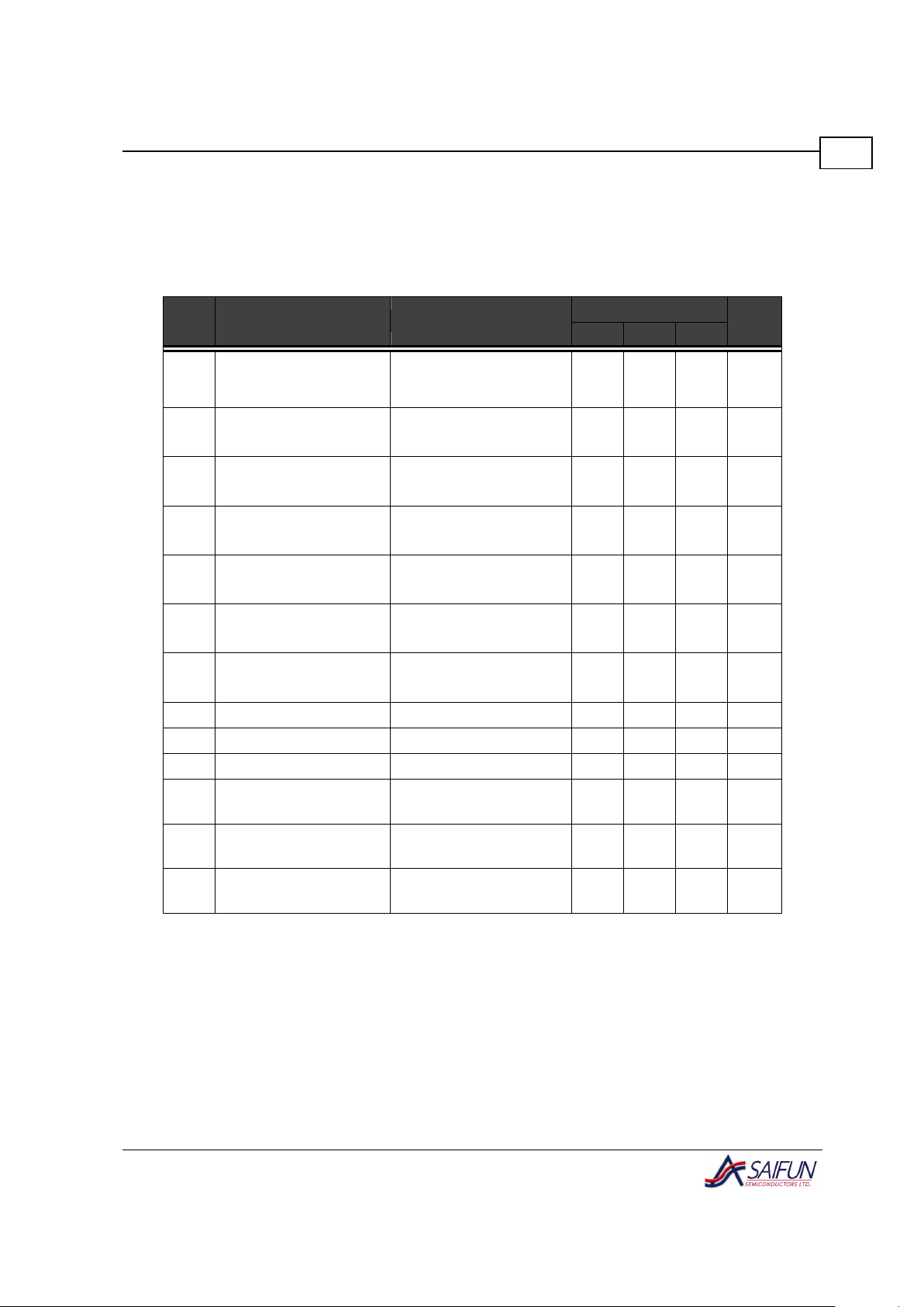
DC Characteristics ........................................................ 9
AC Test Conditions ..................................................... 10
Timing Diagrams......................................................... 11
Signal Description....................................................... 13
Chip Select (CSb).................................................. 13
Serial Clock (SCK) ................................................ 13
Serial Input (SI) ..................................................... 13
Serial Output (SO)................................................. 13
Hold (HOLDb)........................................................ 13
Write Protect (WPb) .............................................. 13
Serial Interface Description........................................ 14
SPI Modes ............................................................ 14
Master........................................................... 14
Slave............................................................. 14
Transmitter/Receiver ..................................... 14
Serial Opcode................................................ 14
Invalid Opcode .............................................. 14
Chip Select (CSb).......................................... 15
Hold Condition............................................... 15
Write Protect ................................................. 16
Functional Description ............................................... 17
Instructions............................................................ 17
Read Status Register (RDSR)............................... 18
Write Enable (WREN) ........................................... 20
Write Disable (WRDI)............................................ 20
Write Status Register (WRSR).............................. 21
Read Data Bytes (READ)...................................... 23
Fast Read (FAST_READ) ..................................... 24
Page Programming (PP) ....................................... 25
Page Erase (PE)................................................... 27
Sector Erase (SE) ................................................. 28
Bulk Erase (BE)..................................................... 29
Software Protection (SP)/ Deep Powerdown (DP) . 30
Release from Software Protect (RES) ................... 31
Release from Software Protection and Read
Electronic Signature (RES).................................... 32
Powerup and Powerdown...................................... 33
Physical Dimensions................................................... 34
Contact Information .................................................... 37
Life Support Policy...................................................... 37
Page 4

SA25F020 Advanced Information
SAIFUN
4
List of Figures
Figure 1. SA25F020 Block Diagram ................................ 5
Figure 2. SOIC 8 (150 mil)/PDIP/MLF Package
(Top View)............................................................. 6
Figure 3. SA25F020 Ordering Information....................... 7
Figure 4. SPI Mode 0 (0,0) Input Timing........................ 11
Figure 5. SPI Mode 0 (0,0) Output Timing..................... 11
Figure 6. AC Measurements I/O Waveform................... 12
Figure 7. Supported SPI Modes .................................... 14
Figure 8. Hold Condition................................................ 15
Figure 9. SPI Serial Interface ........................................ 17
Figure 10. Read Status Register (RDSR) Instruction
Sequence ............................................................ 19
Figure 11. Write Enable (WREN) Instruction Sequence 20
Figure 12. Write Disable (WRDI) Instruction Sequence. 20
Figure 13. Write Status Register (WRSR) Instruction
Sequence ............................................................ 22
Figure 14. Read (READ) Instruction Sequence ............. 23
Figure 15. Fast Read (FAST_READ) Instruction
Sequence ............................................................ 24
Figure 16. Page Programming (PP) Instruction
Sequence ............................................................ 26
Figure 17. Page Erase (PE) Instruction Sequence ........ 27
Figure 18. Sector Erase (SE) Instruction Sequence ...... 28
Figure 19. Bulk Erase (BE) Instruction Sequence.......... 29
Figure 20. Software Protection Instruction Sequence .... 30
Figure 21. Release from Software Protect (RES) Instruction
Sequence ............................................................ 31
Figure 22. Release from Software Protection and Read
Electronic Signature (RES) Instruction Sequence 32
Figure 23. 8-pin SOIC Package..................................... 34
Figure 24. 8-pin MLF Leadless Package ....................... 35
Figure 25. Molded Dual-in-line Package (N) Package
Number N08E...................................................... 36
List of Tables
Table 1. Memory Organization ........................................ 5
Table 2. Pin Names......................................................... 6
Table 3. DC Characteristics............................................. 9
Table 4. AC Test Conditions.......................................... 10
Table 5. AC Measurements........................................... 12
Table 6. Instruction Set ................................................. 17
Table 7. Status Register Format.................................... 18
Table 8. Read Status Register Definition....................... 18
Table 9. Block Write Protect Bits................................... 21
Table 10. WPBEN Operation ........................................ 21
Table 11. Powerup ........................................................ 33
Page 5
SA25F020 Advanced Information
SAIFUN
5
Memory Organization
The memory is organized in the following
manner:
•= 262,144 bytes (8 bits each)
•= 4 sectors (512 Kb, 65,536 bytes
each), as shown in Table 1
•= 1024 pages (256 bytes each)
Each page can be individually
programmed, with the bits programmed
from 1 to 0. The SA25F020's memory can
be erased via the Page, Sector or Bulk
Erase commands, with the bits erased
from 0 to 1.
Table 1. Memory Organization
Sector Address Range
3 30000h 3FFFFh
2 20000h 2FFFFh
1 10000h 1FFFFh
0 00000h 0FFFFh
HOLDb
WPb
Vcc
GND
SO
SI
SCK
CSb
PSSRAM
IO
Array - R
X
D
E
C
Logic
Array - L
DATA PATHRD
Figure 1. SA25F020 Block Diagram
Page 6
SA25F020 Advanced Information
SAIFUN
6
Connection Diagrams
SA25F020
CSb 1
SO 2
WPb 3
GND 4
8
7
6
5
VCC
HOLDb
SCK
SI
Figure 2. SOIC 8 (150 mil)/PDIP/MLF Package (Top View)
Table 2. Pin Names
Pin Name Signal Name
CSb Chip Select
SCK Serial Data Clock
SI Serial Data Input
SO Serial Data Output
GND Ground
VCC Power Supply
WPb Write Protect
HOLDb Suspend Serial Input
Page 7
SA25F020 Advanced Information
SAIFUN
7
Ordering Information
LXXF25SA Letter
L
020
F
25
SA
Interface
Density
Voltage Operating Range
Description
2.7 V to 3.6 V
2 Mb with Write Protect
Flash
SPI-2 Wires
Saifun Non-Volatile
Memory
X
Blank
X
Tube
Tape and Reel
PP
Package
N
M8
MLF
8-pin DIP
8-pin SOIC (150 mil)
8-lead MLF
F
Blank
F
Non-lead Free
Lead Free
E
Blank
E
Temp. Range 0 to 70 C
-40 to +85 C
o
o
Figure 3. SA25F020 Ordering Information
Page 8

SA25F020 Advanced Information
SAIFUN
8
Product Specifications
Absolute Maximum Ratings
Storage Temperature
-65
°C to +150 °C
All input or output voltages with
respect to Ground
4.5 V to -0.3 V
Lead Temperature
(Soldering, 10 seconds)
+235
°C
ESD Rating 2000 V min.
ESD/Latch Up Specification (JEDEC 8 Spec)
Human Body Model Minimum 4 KV
Machine Model Minimum 500 V
Charge Device Model Minimum 1 KV
Latch Up
100 mA on all pins +125
°C
Operating Conditions
Operating Temperature:
SA25F020
SA25F020E
0
°C to +70 °C
-40
°C to +85 °C
Positive Power Supply:
SA25F020
2.7 V to 3.6 V
Page 9
SA25F020 Advanced Information
SAIFUN
9
DC Characteristics
Applicable over recommended operating range from TAI = -40 ºC to 85 ºC, VCC = 2.7-3.6 V.
Table 3. DC Characteristics
Limits
Symbol Parameter Test Conditions
Min Typ* Max
Unit
VCC
Supply Voltage 2.7 3 3.6
V
I
CC1
Active Power Supply
Current (Read)
SCK = 0.1V
CC
/0.9 VCC @
25 MHz
9 12
mA
I
CC2
Active Power Supply
Current (Page Program)
CSb = VCC 15 mA
I
CC3
Active Power Supply
Current (WRSR)
CSb = VCC 15 mA
I
CC4
Active Power Supply
Current (SE)
CSb = VCC 15 mA
I
CC5
Active Power Supply
Current (BE)
CSb = VCC 15 mA
ISB Standby Current
V
CC
= 3.0 V,
CSb = V
CC
1
µA
IIL
Input Leakage Current V
IN
= GND to VCC 1
µA
IOL
Output Leakage Current V
IN
= GND to VCC 1
µA
VIL
Input Low Voltage -0.3 0.3 V
CC
V
VIH
Input High Voltage 0.7 V
CC
V
CC
+
0.5
V
VOH
Output High Voltage I
OH
= -0.1 mA
VCC -
0.2
V
VOL
Output Low Voltage I
OL
= 1.6 mA; VCC = 2.7 V 0.4
V
*Typical values are at TAI = 25 ºC and 3 V.
Page 10
SA25F020 Advanced Information
SAIFUN
10
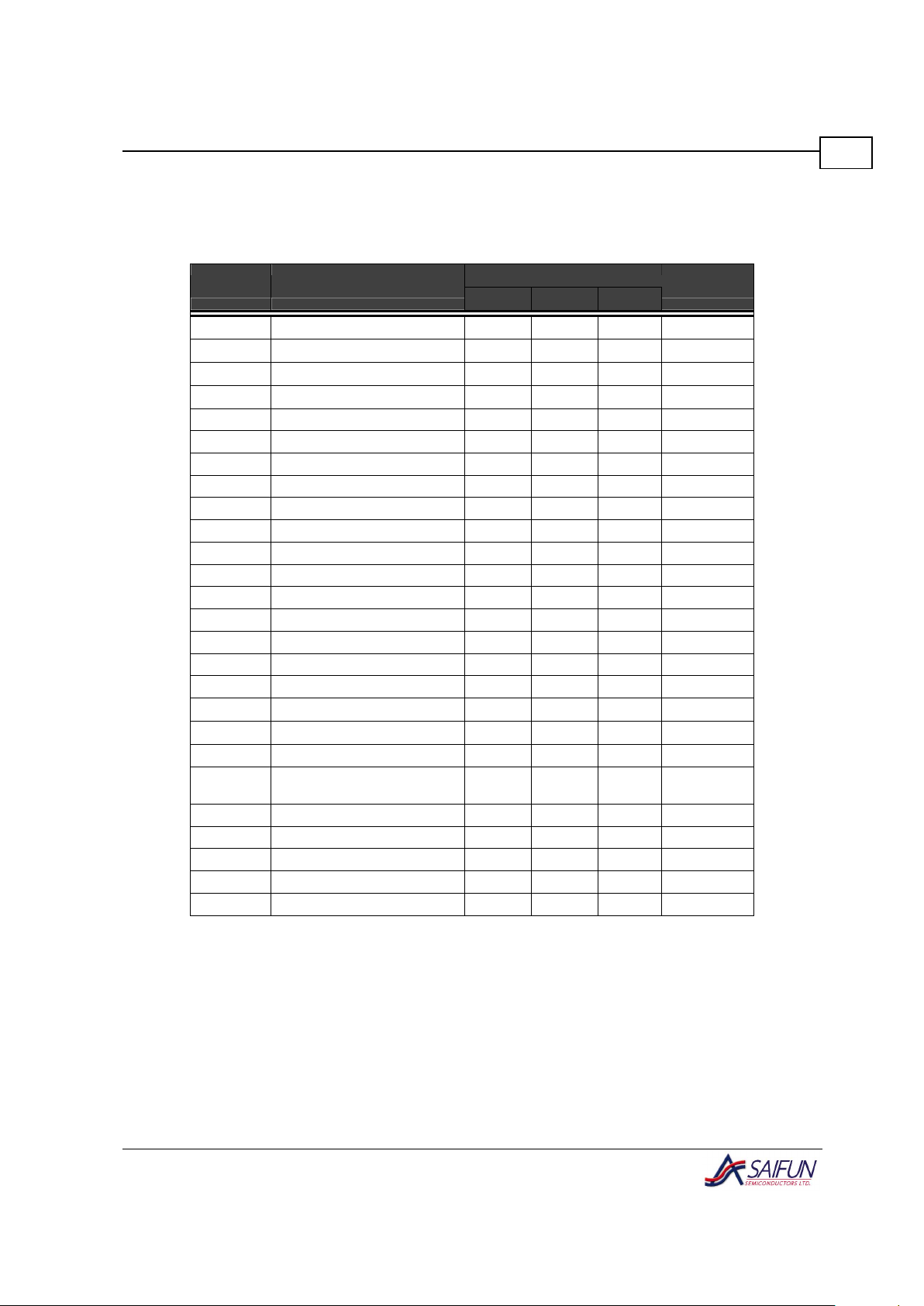
AC Test Conditions
Table 4. AC Test Conditions
25 MHz
Symbol Parameter
Min Typ Max
Unit
F
SCK
SCK Clock Frequency D.C. 25 MHz
t
CRT
Clock Rise Time (Slew Rate) 0.1
V/ns
t
CFT
Clock Fall Time (Slew Rate) 0.1
V/ns
t
WH
SCK High Time 18
ns
t
WL
SCK Low Time 18 ns
tCS CSb High Time 100 ns
t
CSS
**
CSb Setup Time 10 ns
t
CSH
**
CSb HOLD Time 10 ns
t
HD
**
HOLDb Setup Time 10 ns
t
CD
**
HOLDb Hold Time 10 ns
tV Output Valid 0 15 ns
tHO Output Hold Time 0 ns
t
HD:DAT
Data in Hold Time 5 ns
t
SU:DAT
Data in Setup Time 5 ns
t
LZ
**
HOLDb to Output Low Z 15 ns
t
HZ
**
HOLDb to Output High Z 20 ns
t
DIS
**
Output Disable Time 15 ns
t
WPS
**
Write Protect Setup Time 20
ns
t
WPH
**
Write Protect Hold Time 100
ns
tPP* 256-byte Page Programming 8 10 ms
tEP*
Page Erase and
Programming
10 15 ms
tPE Page Erase Time 3 6 ms
tSE Sector Erase Time 0.5 0.8 sec
tBE Bulk Erase Time 2 3 sec
t
RES
Release SP Mode 1000 ns
Endurance 100K Erase cycles
* 256 bytes in the checkerboard programming formation.
** Value guaranteed by characterization, not 100% tested in production
Page 11
SA25F020 Advanced Information
SAIFUN
11
Timing Diagrams
All timing diagrams are based on SPI protocol modes 0 and 1.
SCK
SI
CS
t
CSH
t
CSH
t
CSS
t
CSS
MSB IN
t
SU:DATtHD:DAT
t
CRT
t
CFT
LSB IN
t
CS
SO
High Impedance
Figure 4. SPI Mode 0 (0,0) Input Timing
SCK
CS
t
WL
t
V
t
WH
LSB OUT
SO
t
HO
t
V
t
HO
t
DIS
Figure 5. SPI Mode 0 (0,0) Output Timing
Page 12
SA25F020 Advanced Information
SAIFUN
12
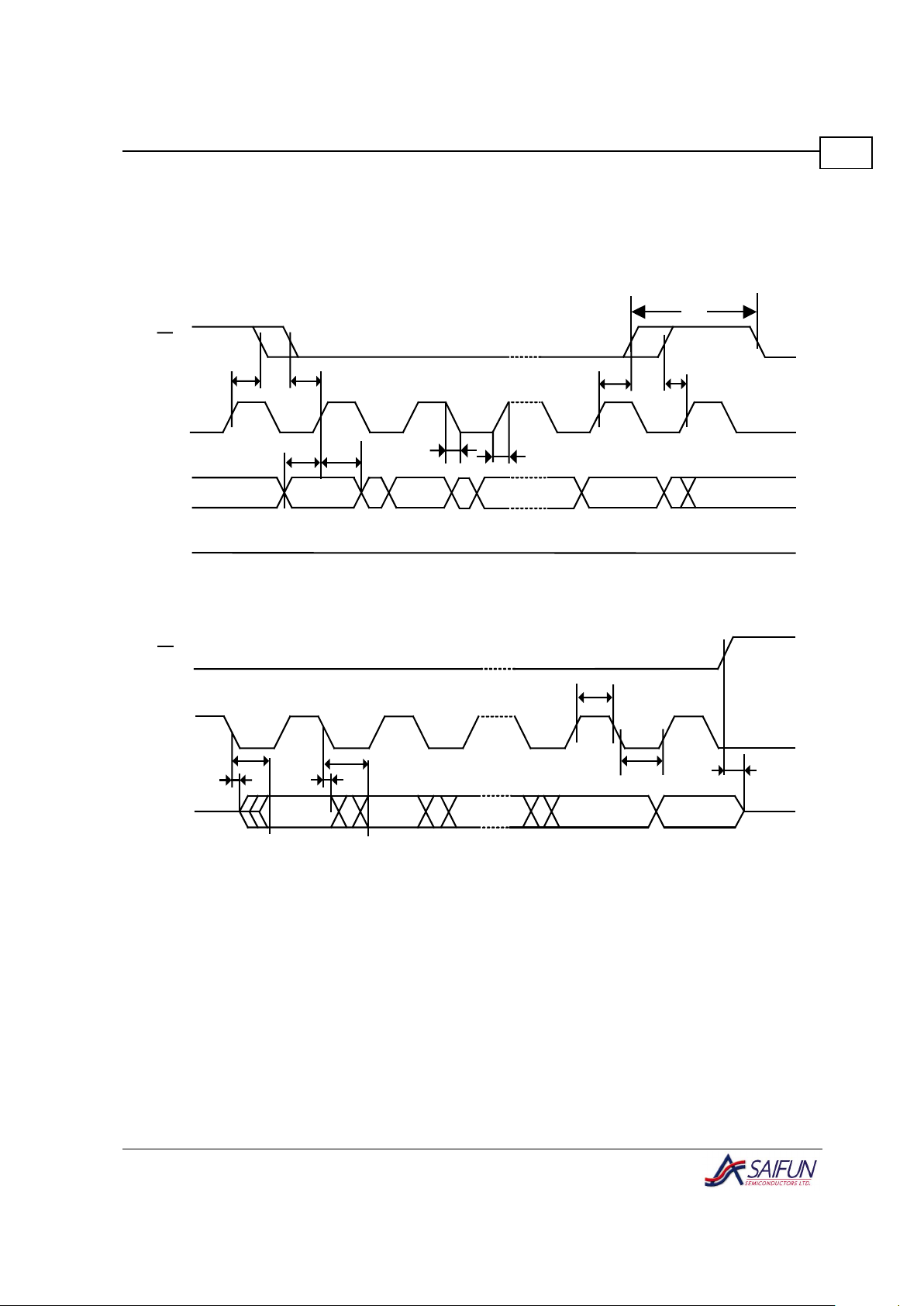
0.7Vcc
0.2Vcc
0.8Vcc
0.3Vcc
Input Levels
Input and Output
Timing Reference Levels
Figure 6. AC Measurements I/O Waveform
Table 5. AC Measurements
Symbol Parameter Min Max Unit
C
L
Load Capacitance 30 pF
Input Rise and Fall Times 5 ns
Input Pulse Voltage 0.2 VCC to 0.8 VCC V
Input and Output Timing
Reference Voltages
0.3 VCC to 0.7 VCC V
Page 13

SA25F020 Advanced Information
SAIFUN
13
Signal Description
Chip Select (CSb)
This is an active-low input pin to the device
that is generated by the master controlling
the device. A low level on this pin selects
the device, while a high level deselects the
device. All serial communications with the
device are enabled only when this pin is
held low.
Serial Clock (SCK)
This is an input pin to the device that is
generated by the master controlling the
device. It is a clock signal that
synchronizes the communication between
a master and the device. All input
information (SI) to the device is latched on
the rising edge of this clock input, while
output data (SO) from the device is driven
after the falling edge of this clock input.
Serial Input (SI)
This is an input pin to the device that is
generated by the master controlling the
device. The master transfers input
information (instruction, addresses and the
data to be programmed) into the device
serially via this pin. This input information is
latched on the rising edge of the SCK.
Serial Output (SO)
This is an output pin from the device that is
used to transfer output data to the
controlling master. Output data is serially
shifted out on this pin after the falling edge
of the SCK.
Hold (HOLDb)
This is an active low input pin to the device
that is generated by the master controlling
the device. When driven low, this pin
suspends any current communication with
the device. The suspended communication
can be resumed by driving this pin high.
This feature eliminates the need to
re-transmit the entire sequence by
enabling the master to resume the
communication from where it was left off.
This pin should be tied high if this feature is
not used. Refer to Hold Condition,
page 15, for additional details.
Write Protect (WPb)
This is an active low input pin to the device.
This pin allows enabling and disabling of
writes to the device's memory array and
status register. When this pin is held low,
writes to the memory array and status
register are disabled; when it is held high,
they are enabled. Refer to Write Protect,
page 16, for additional details.
Page 14

SA25F020 Advanced Information
SAIFUN
14
Serial Interface
Description
SPI Modes
These devices can be driven by a
microcontroller with its SPI peripheral
running in either of the two following
modes:
•= CPOL=0, CPHA=0
•= CPOL=1, CPHA=1
In both of these modes, input data is
latched on the rising edge of SCK, and
output data is available from the falling
edge of SCK. The difference between the
two modes, as shown in Figure 7, is the
clock polarity when the bus master is in
Standby mode and is not transferring data,
as follows:
•= SCK remains at 0 for CPOL = 0,
CPHA = 0
•= SCK remains at 1 for CPOL = 1,
CPHA = 1
MSB
MSB
CS
CS
SO
SI
0
1
0
1
CPOL CPHA
Figure 7. Supported SPI Modes
Master
The device that generates the SCK.
Slave
As the SCK pin is always an input, the
SA25F020 always operates as a slave.
Transmitter/Receiver
The SA25F020 has separate pins
designated for data transmission and
reception.
Serial Opcode
The first byte is received after the device is
selected. This byte contains the opcode
that defines the operation to be performed
(for more details, refer to Table 6,
page 17).
Invalid Opcode
If an invalid opcode is received, no data is
shifted into the SA25F020, and the serial
output pin remains in a high impedance
state until a CSb falling edge is detected
again, which reinitializes the serial
communication.
Page 15

SA25F020 Advanced Information
SAIFUN
15
Chip Select (CSb)
The SA25F020 is selected when the CSb
pin is low. When the device is not selected,
data is not accepted via the SI pin, and the
SO pin remains in a high impedance state.
Hold Condition
The HOLDb pin is used in conjunction with
the CSb pin to select the SA25F020. When
the device is selected and a serial
sequence is underway, HOLDb can be
used to pause the serial communication
with the master device without resetting the
serial sequence.
To enter the hold condition the device must
be selected, with CSb low.
As shown in Figure 8, the Hold condition
starts on the falling edge of the HOLDb
signal, provided that SCK is low. The Hold
condition ends on the rising edge of the
HOLDb signal, provided that SCK is low. If
the falling edge does not coincide with SCK
being low, the Hold condition starts only
after SCK next goes low.
Similarly, if the
rising edge does not coincide with SCK
being low, the Hold condition ends only
after SCK next goes low.
During the Hold condition, SO is high
impedance, and SI and SCK are Don’t
Care. In most cases, the device is kept
selected, with CSb driven low, for the entire
duration of the Hold condition, which
ensures that the internal logic state
remains unchanged from the moment it
enters the Hold condition.
NOTE:
Driving CSb high while HOLDb is still
low is not a legal operation.
Hold
Condition
(Standard Use)
Hold
Condition
(Non-Standard Use)
SCK
HOLD
Figure 8. Hold Condition
Page 16

SA25F020 Advanced Information
SAIFUN
16
Write Protect
The WPb pin enables write operations to
the status register when held high. When
the WPb pin is brought low and the
WPBEN bit is 1, all write operations to the
status register are inhibited (for more
details, refer to Table 10, page 21). If WPb
goes low while CSb is still low, the write to
the status register is interrupted. If the
internal write cycle has already been
initiated, WPb going low has no effect on
any write operations to the status register.
The WPb pin function is blocked when the
WPBEN bit in the status register is 0,
which enables the user to install the
SA25F020 in a system with the WPb pin
tied to ground but still able to write to the
status register. All WPb pin functions are
enabled when the WPBEN bit is set to 1.
Page 17

SA25F020 Advanced Information
SAIFUN
17
Functional Description
Instructions
Figure 9 presents a schematic diagram of
the SA25F020's SPI serial interface.
SI
SO
CSb
SCK
SI
SO
CSb
SCK
SI
SO
CSb
SCK
DATA OUT
DATA IN
SERIAL CLOC K
SSO
SS1
SS2
SS3
MASTER :
MICR OCONTROLL ER
SLAVE
SA25F020
SI
SO
CSb
SCK
Figure 9. SPI Serial Interface
The SA25F020's SPI consists of an 8-bit
instruction register that decodes a specific
instruction to be executed. Thirteen
different instructions (called opcodes) are
incorporated in the device for various
operations. Table 6 lists the instruction set
and the format for proper operation. All
opcodes, array addresses and data are
transferred in an MSB-first-LSB-last
fashion. Detailed information about each of
these opcodes is provided for the individual
instruction descriptions in the sections that
follow.
Table 6. Instruction Set
Instruction
Name
Instruction
Format
Operation
WREN 0000 0110
Set Write Enable
Latch
WRDI 0000 0100
Reset Write Enable
Latch
RDSR 0000 0101
Read Status
Register
WRSR 0000 0001
Write Status
Register
READ 0000 0011
Read Data from
Memory Array
FAST_READ 0000 1011
Read Data from
Memory Array
Page
Program
0000 0010
Write Data to
Memory Array
PE 1000 0001 Page Erase
SE 1101 1000 Sector Erase
BE 1100 0111 Bulk Erase
SP 1011 1001 Software Protect
1010 1011
Release from
Software Protect
Mode
RES
1010 1011
+3 dummy bytes
Release from
Software Protect +
Read ID
READ_ID
1010 1011
+3 dummy bytes
Read ID
Page 18

SA25F020 Advanced Information
SAIFUN
18
In addition to the instruction register, the
device also contains an 8-bit status register
that can be accessed by RDSR and WRSR
instructions. The byte defines the Block
Write Protection (BP1 and BP0) levels,
Write Enable (WEN) status, Busy/Rdy
(/RDY) status and Hardware Write Protect
(WPBEN) status of the device. Table 7
illustrates the format of the status register.
Table 7. Status Register Format
Bit 7 Bit 6 Bit 5 Bit 4 Bit 3 Bit 2 Bit1 Bit 0
WPBEN X X X BP1 BP0 WEN /RDY
Read Status Register (RDSR)
The RDSR instruction provides read
access to the status register. The
BUSY/RDY and WREN statuses of the
device can also be determined by this
instruction. In addition, the Block Write
Protection bits indicate the extent of
protection employed. In order to determine
the status of the device, the value of the
/RDY bit can be continuously polled before
sending any write instruction.
Table 8. Read Status Register Definition
Bit Definition
Bit 0 (/RDY)
Bit 0 = 0 (/RDY) indicates that the
device is READY.
Bit 0 = 1 indicates that a write
cycle is in progress.
Bit 1 (WEN)
Bit 1 = 0 indicates that the device
is not write enabled.
Bit 1 = 1 indicates that the device
is write enabled.
Bit 2 (BP0) Block Write Protect Bit 0
Bit 3 (BP1) Block Write Protect Bit 1
Bit 7
(WPBEN)
Write Protect Mode Enable Bit
Bit 7 (WPBEN) is Hardware Write Protect
mode. If this bit is a 1, this mode is enabled
and the status register is write protected.
Bits 6 through 4 are always 0.
Bit 3 (BP1) and Bit 2 (BP0) together
indicate a Block Write Protection previously
sent to the device.
Bits 0 and 1 are 1 during an internal write
cycle.
Bit 1 (WEN) indicates the Write Enable
status of the device. This bit is read by
executing an RDSR instruction. If this bit is
1, the device is write enabled; if it is 0, it is
write disabled.
Bit 0 (/RDY) indicates the Busy/Ready
status of the device. This bit is a read-only
bit and is read by executing an RDSR
instruction. If this bit is 1, the device is busy
doing a Program or Erase cycle; if it is 0,
the device is ready.
Page 19

SA25F020 Advanced Information
SAIFUN
19
The RDSR command requires the following
sequence:
1. The CSb pin is pulled low to select
the device and the RDSR opcode is
transmitted on the SI pin.
2. The data on the SI pin becomes
Don't Care.
3. The data from the status register is
shifted out on the SO pins, with the
D7 bit first and the D0 bit last, as
shown in Figure 10.
1 32109876540 14131211
Instruction
132 07654
SCK
SO
High Impedanc e
MSB
Status Register Out
SI
15 181716 22212019
132 07654
MSB
Status Register Out
23
7
MSB
CS
Figure 10. Read Status Register (RDSR) Instruction Sequence
Page 20

SA25F020 Advanced Information
SAIFUN
20
Write Enable (WREN)
The device powers up in the Write Disable
state when V
CC
is applied. All programming
instructions must be preceded by a WREN
instruction. The instruction sequence is
shown in Figure 11, with SO in high
impedance.
Write Disable (WRDI)
To protect the device against inadvertent
writes, the WRDI instruction disables all
programming modes. The WRDI
instruction is independent of the WP pin's
status. The WREN instruction should be
executed after the WRDI instruction to
re-enable all programming modes. The
instruction sequence is shown in Figure 12,
with SO in high impedance.
3276540
Instruction
SCK
SI
1
CS
Figure 11. Write Enable (WREN) Instruction Sequence
3276540
Instruction
SCK
SI
1
CS
Figure 12. Write Disable (WRDI) Instruction Sequence
Page 21

SA25F020 Advanced Information
SAIFUN
21
Write Status Register (WRSR)
The WRSR instruction enables the user to
select one of four levels of protection. The
SA25F020 is divided into four array
segments. The top quarter, top half or all of
the memory segments can be protected
(for more details, refer to Table 9). The
data within a selected segment is therefore
read-only.
Table 9. Block Write Protect Bits
Status Register Bits
Level
BP1 BP0
Array Addresses
Protected
0 0 0
None
1/4 0 1
30000 - 3FFFF
1/2 1 0
20000 - 3FFFF
All 1 1
00000 - 3FFFF
The WRSR instruction (as shown in
Table 10) also allows the user to enable or
disable the WPb pin via the WPBEN bit.
Hardware write protection is enabled when
the WPb pin is low and the WPBEN bit is
1, and disabled when either the WP pin is
high or the WPBEN bit is 0. When the
device is hardware write protected, writes
to the status register are disabled.
NOTE:
When the WPBEN bit is hardware write
protected, it cannot be changed back
to 0 while the WPb pin is held low.
Table 10. WPBEN Operation
WPb WPBEN WEN
Protected
Blocks
Un-
protected
Blocks
Status
Register
X 0 0 Protected Protected Protected
X 0 1 Protected Writeable Writeable
Low 1 0 Protected Protected Protected
Low 1 1 Protected Writeable Protected
High X 0 Protected Protected Protected
High X 1 Protected Writeable Writeable
The WRSR instruction is enabled:
1. When the WPb pin is held high and
the device has been previously write
enabled via the WREN instruction.
2. When the WPb pin is held low, the
WPBEN bit is 0 and the device has
been previously write enabled via the
WREN instruction.
Page 22

SA25F020 Advanced Information
SAIFUN
22
The WRSR command requires the
following sequence:
1. The CSb pin is pulled low to select
the device.
2. The WRSR opcode is then
transmitted on the SI pin, followed
by the data to be programmed.
The instruction sequence is shown in
Figure 13.
Instruction Status Register In
1 32109876540 14131211 15
132 07654
SCK
SI
SO
MSB
High Impedance
CS
Figure 13. Write Status Register (WRSR) Instruction Sequence
Page 23

SA25F020 Advanced Information
SAIFUN
23
Read Data Bytes (READ)
Reading the memory via the serial SPI link
requires the following sequence:
1. After the CSb line is pulled low to
select the device, the READ
opcode is transmitted via the SI
line, followed by the 3-byte address
to be read (address bits A23 to A18
are Don’t Care).
2. Upon completion, any data on the
SI line is ignored.
3. The data (D7-D0) at the specified
address is then shifted out onto the
SO line. Each bit is shifted out at a
maximum SCK frequency of F
SCK
.
If only one byte is to be read, the CSb line
should be driven high after the data comes
out. The READ sequence can be
continued, as the byte address is
automatically incremented and data
continues to shift out. When the highest
address is reached, the address counter
rolls over to the lowest address, enabling
the entire memory to be read in one
continuous READ cycle. The instruction
sequence is shown in Figure 14.
Driving CSb high terminates the READ
instruction, which can be done at any time
during data output. Any READ instruction
executed while an Erase, Program or
WRSR cycle is in progress is rejected
without having any effect on the cycle in
progress.
1 32109876540 31302928
Instruction
24-Bit
Address
23 2122 132
0
132 07654
3635343332 393837
SCK
SI
SO
High Impedance
MSB
DATA OUT 1 DATA OUT 2
7
MSB
CS
Figure 14. Read (READ) Instruction Sequence
Page 24

SA25F020 Advanced Information
SAIFUN
24
Fast Read (FAST_READ)
The Fast Read instruction is included in the
device in order for it to be compatible with
other SPI Flash devices. Both the READ
and FAST_READ instructions read the
memory at the specified SCK frequency
(F
SCK
), with a maximum speed of 25 MHz.
Reading the memory via the serial SPI link
requires the following sequence:
1. After the CSb line is pulled low to
select the device, the READ
opcode is transmitted via the SI
line, followed by the 3-byte address
and a dummy byte (address bits
A23 to A18 are Don’t Care).
2. Upon completion, any data on the
SI line is ignored.
3. The data (D7-D0) at the specified
address is then shifted out onto the
SO line. Each bit is shifted out at a
maximum frequency of F
SCK
.
If only one byte is to be read, the CSb line
should be driven high after the data comes
out. The READ sequence can be
continued, as the byte address is
automatically incremented and data
continues to shift out. When the highest
address is reached, the address counter
rolls over to the lowest address, enabling
the entire memory to be read in one
continuous READ cycle. The instruction
sequence is shown in Figure 15.
Driving CSb high terminates the
FAST_READ instruction, which can be
done at any time during data output. Any
FAST_READ instruction executed while an
Erase or Program cycle is in progress is
rejected without having any effect on the
cycle in progress.
1 3210987654031302928
Instruction
24-Bit
Address
23 2122 132 0
132 07654
3635343332 393837
132 07654
Dummy Byte
4443424140 474645
DATA OUT 1
DATA OUT 2
SCK
SI
SO
MSB
High Impedance
7
MSB
CS
Figure 15. Fast Read (FAST_READ) Instruction Sequence
Page 25

SA25F020 Advanced Information
SAIFUN
25
Page Programming (PP)
The PP instruction allows bytes to be
programmed in the memory (changing bits
from 1 to 0). In order to program to the
SA25F020, two separate instructions must
be executed. The device must first be write
enabled via the WREN instruction, and
then a PP sequence (which consists of four
bytes plus data) may be executed. The
address of the memory locations to be
written must be outside the protected
address field location selected by the Block
Write Protection level. During an internal
Program cycle, all commands are ignored
except the RDSR instruction.
A PP instruction requires the following
sequence:
•= After the CSb line is pulled low to
select the device, the PP opcode is
transmitted via the SI line, followed
by the byte address and the data
(D7-D0) to be written.
Programming starts after the CSb pin is
brought high. The CSb pin's low-to-high
transition must occur during the SCK low
time, immediately after the clock in the D0
(LSB) data bit. The instruction sequence is
shown in Figure 16, page 26.
As soon as CSb is driven high, the
self-timed PP cycle (whose duration is
defined as T
PP
) is initiated. While the Page
Program cycle is in progress, the status
register may be read to check the value of
the Write in Progress (/RDY) bit. The /RDY
bit is 1 during the self-timed Page Program
cycle, and 0 when it is completed. The
Write Enable Latch (WEN) bit is reset at
some unspecified time before the cycle is
completed.
The SA25F020's PP operation is capable
of up to a 256-byte programming, from 1 to
256 bytes at a time (changing bits from 1 to
0), provided that they lie in consecutive
addresses on the same page of memory.
After each byte is received, the eight
low-order address bits are internally
incremented by one. If more than 256
bytes of data are transmitted, the address
counter rolls over and the previously
written data is overwritten. The SA25F020
is automatically returned to the write
disable state at the completion of a Write
cycle.
NOTES:
1. If the device is not write enabled,
the device ignores the PP
instruction and returns to the
standby state when CSb is brought
high. A new CSb falling edge is
required to re-initiate the serial
communication.
2. A PP instruction applied to a page
that is protected by the Block
Protect (BP1, BP0) bits (as
described in Table 8, page 18, and
Table 9, page 21) is not executed.
Page 26

SA25F020 Advanced Information
SAIFUN
26
1 3210987654031302928
Instruction
24-Bit
Address
23 2122 132 0
3635343332 393837
132 07654
Data Byte 1
2072
132 07654
Data Byte 2
4443424140 474645 5251594948 555453
132 07654
Data Byte 3
2079
2078
2077
2076
2075
2074
2073
Data Byte 256
SCK
SI
SCK
SI
MSB
MSBMSB
MSB
MSB
CS
CS
132 07654
Figure 16. Page Programming (PP) Instruction Sequence
Page 27

SA25F020 Advanced Information
SAIFUN
27
Page Erase (PE)
The PE instruction sets all 256 bytes in the
selected page to 1. Before it can be
executed, two separate instructions must
be carried out. The device must first be
write enabled via the WREN instruction,
and then a PE sequence, which consists of
one opcode byte and three data bytes may
be executed. The address of the memory
locations to be written must be inside the
page to be erased and outside the
protected address field location selected by
the Block Write Protection level. During an
internal PE cycle, all commands are
ignored except the RDSR instruction.
A PE instruction requires the following
sequence:
1. After the CSb line is pulled low to
select the device, the PE opcode is
transmitted via the SI line, followed
by the 3-byte address.
2. Erasing begins after the CSb pin is
brought high. The CSb pin's
low-to-high transition must occur
during the SCK low time,
immediately after the clock in the
last address bit.
As soon as CSb is driven high, the
self-timed PE cycle (whose duration is
defined as T
PE
) is initiated. While the PE
cycle is in progress, the status register may
be read to check the value of the /RDY bit.
The /RDY bit is 1 during the self-timed PE
cycle, and 0 when it is completed. The
WEN bit is reset at some unspecified time
before the cycle is completed. The
instruction sequence is shown in Figure 17.
The SA25F020 is automatically returned to
the Write Disable state at the completion of
a PE cycle.
NOTES:
1. If the device is not write enabled,
the device ignores the PE
instruction and returns to the
standby state when CSb is brought
high. A new CSb falling edge is
required to re-initiate the serial
communication.
2. A PE instruction applied to a page
that is protected by the Block
Protect (BP1, BP0) bits (as
described in Table 8, page 18, and
Table 9, page 21) is not executed.
1 32109876540 31302928
Instruction 24 Bit Address
132 0
SCK
SI
MSB
CS
232122
Figure 17. Page Erase (PE) Instruction Sequence
Page 28

SA25F020 Advanced Information
SAIFUN
28
Sector Erase (SE)
The SE instruction sets all 512 Kb in the
selected sector to 1. Before it can be
executed, two separate instructions must
be carried out. The device must first be
write enabled via the WREN instruction,
and then a SE sequence, which consists of
four bytes, may be executed. The address
of the memory locations to be written must
be inside the sector to be erased and
outside the protected address field location
selected by the Block Write Protection
level. During an internal SE cycle, all
commands are ignored except the RDSR
instruction.
A SE instruction requires the following
sequence:
1. After the CSb line is pulled low to
select the device, the SE opcode is
transmitted via the SI line, followed
by the 3-byte address.
2. Erasing begins after the CSb pin is
brought high. The CSb pin's
low-to-high transition must occur
during the SCK low time,
immediately after the clock in the
last address bit.
As soon as CSb is driven high, the
self-timed SE cycle (whose duration is
defined as T
SE
) is initiated. While the SE
cycle is in progress, the status register
may be read to check the value of the
/RDY bit. The /RDY bit is 1 during the
self-timed SE cycle, and 0 when it is
completed. The WEN bit is reset at some
unspecified time before the cycle is
completed. The instruction sequence is
shown in Figure 18.
The SA25F020 is automatically returned to
the write disable state at the completion of
an SE cycle.
NOTES:
1. If the device is not write enabled,
the device ignores the SE
instruction and returns to the
standby state when CSb is brought
high. A new CSb falling edge is
required to re-initiate the serial
communication.
2. A SE instruction applied to a sector
that is protected by the Block
Protect (BP1, BP0) bits (as
described in Table 8, page 18, and
Table 9, page 21) is not executed.
1 32109876540 31302928
Instruction 24 Bit Address
23
2122
132 0
SCK
SI
MSB
CS
Figure 18. Sector Erase (SE) Instruction Sequence
Page 29

SA25F020 Advanced Information
SAIFUN
29
Bulk Erase (BE)
The BE instruction sets all bits in the
memory array to 1. Before it can be
executed, two separate instructions must
be carried out. The device must first be
write enabled via the WREN instruction,
and then a BE sequence, which consists of
four bytes plus data, may be executed. The
address of the memory locations to be
written must be outside the protected
address field location selected by the Block
Write Protection level. During an internal
BE cycle, all commands are ignored except
the RDSR instruction.
A BE instruction requires the following
sequence:
1. After the CSb line is pulled low to
select the device, the BE opcode is
transmitted via the SI line.
2. Erasing begins after the CSb pin is
brought high. The CSb pin's
low-to-high transition must occur
during the SCK low time,
immediately after the clock in the
last opcode bit.
As soon as CSb is driven high, the
self-timed BE cycle (whose duration is
defined as T
BE
) is initiated. While the BE
cycle is in progress, the status register may
be read to check the value of the /RDY bit.
The /RDY bit is 1 during the self-timed BE
cycle, and 0 when it is completed. The
WEN bit is reset at some unspecified time
before the cycle is completed. The
instruction sequence is shown in Figure 19.
The SA25F020 is automatically returned to
the Write Disable state at the completion of
a BE cycle.
NOTES:
1. If the device is not write enabled,
the device ignores the BE
instruction and returns to the
standby state when CSb is brought
high. A new CSb falling edge is
required to re-initiate the serial
communication.
2. A BE instruction can be applied
only if both Block Protect (BP1,
BP0) bits (as described in Table 8,
page 18, and Table 9, page 21)
are 0.
3276540
Instruction
SCK
SI
1
CS
Figure 19. Bulk Erase (BE) Instruction Sequence
Page 30

SA25F020 Advanced Information
SAIFUN
30
Software Protection (SP)/
Deep Powerdown (DP)
The DP instruction is included in the device
in order to be compatible with other SPI
Flash devices, and is identical to the SP
instruction.
The SA25F020's low standby current of
1 µA is the same in both DP and Standby
modes. It is recommended that the
standard Standby mode be used for the
lowest power current draw, as well as an
extra SP mechanism while the device is
not in active use. This is due to the fact
that while in this mode, the device ignores
all Write, Program and Erase instructions.
The SP instruction is entered by driving
CSb low, followed by the instruction code
on the SI pin. CSb must be driven low for
the entire duration of the sequence. The
instruction sequence is shown in Figure 20.
CSb must be driven high after the eighth
bit of the instruction code has been latched
in; otherwise, the SP instruction is not
executed. As soon as CSb is driven high, it
requires a delay of t
DP
before SP mode is
entered.
Once the device has entered SP mode, all
instructions are ignored except the Release
from Software Protect and Read Electronic
Signature (RES) instructions, which
release the device from this mode. RES
instructions also enable the Electronic
Signature to be read on the SO pin.
SP mode automatically stops at
powerdown, and the device always powers
up in the Standby mode. Any SP
instruction executed while an Erase,
Program or WRSR cycle is in progress is
rejected without having any effect on the
cycle in progress.
1 3276540
Instruction
SCK
SI
t
DP
Software Protect ModeStandby Mode
CS
Figure 20. Software Protection Instruction Sequence
Page 31

SA25F020 Advanced Information
SAIFUN
31
Release from Software Protect
(RES)
Once the device has entered SP mode, all
instructions are ignored except the RES
mode.
Any RES instruction executed while an
Erase, Program or Write Status Register
cycle is in progress is not decoded, and
has no effect on the cycle that is in
progress.
The device is first selected by driving CSb
low, followed by an 8-bit instruction byte,
with each bit being latched in on SI during
the rising edge of SCK.
Driving CSb high after the 8-bit instruction
byte has been received by the device, but
before the whole of the 8-bit Electronic
Signature has been transmitted for the first
time (as shown in Figure 21), will still
ensure that the device is put into Standby
mode. The transition to Standby mode is
delayed by t
RES
, and CSb must remain high
for at least t
RES
(max), as specified in
Table 4 on page 10. Once in Standby
mode, the device waits to be selected, so
that it can receive, decode and execute
instructions.
1 3276540
Instruction
SCK
SI
t
RES
Software Protect Mode
Standby Mode
CS
Figure 21. Release from Software Protect (RES) Instruction Sequence
Page 32

SA25F020 Advanced Information
SAIFUN
32
Release from Software
Protection and Read Electronic
Signature (RES)
Once the device has entered SP mode, all
instructions are ignored except the RES
mode. The instruction can also be used to
read the 8-bit Electronic Signature of the
device on the SO pin.
The RES instruction always provides
access to the Electronic Signature of the
device (except while an Erase, Program or
Write Status Register cycle is in progress),
and can be applied even if SP mode has
not been entered. Any RES instruction
executed while an Erase, Program or Write
Status Register cycle is in progress is not
decoded, and has no effect on the cycle in
progress.
This instruction serves a second purpose
as well. The device features an 8-bit
Electronic Signature, whose value for the
SA25F020 is 11h. This can be read using
the RES instruction.
The device is first selected by driving CSb
low. The instruction code is followed by
three dummy bytes, each bit being latched
in on SI during the rising edge of SCK.
The 8-bit Electronic Signature, which
stored in the memory, is then shifted out on
SO, with each bit being shifted out during
the falling edge of SCK. The instruction
sequence is shown in Figure 22.
Driving CSb high after the Electronic
Signature has been read at least once
terminates the RES instruction. Sending
additional clock cycles on SCK, while CSb
is driven low causes the Electronic
Signature to be output repeatedly.
When CSb is driven high, the device is put
into Standby mode. The transition to
Standby mode is delayed by t
RES
, and CSb
must remain high for at least t
RES
(max), as
specified in Table 4 on page 10. Once in
Standby mode, the device waits to be
selected, so that it can receive, decode and
execute instructions.
1 32109876540 31302928
Instruction
3 Dummy
Bytes
23 2122 132 0
3635343332 393837
SCK
SI
SO
High Impeda nce
MSB
Electonic ID
MSB
t
RES
Software Protect Mode Standby Mode
132 07654
CS
Figure 22. Release from Software Protection and Read Electronic Signature (RES) Instruction
Sequence
Page 33

SA25F020 Advanced Information
SAIFUN
33
Powerup and Powerdown
The device must not be selected at
powerup or powerdown (that is, CSb must
follow the voltage applied on V
CC
) until VCC
reaches the correct value, as follows:
•= V
CC
(min) at powerup, and then for a
further delay of t
PU
(as described in
Table 11)
•= V
SS
at powerdown
A simple pull-up resistor on CSb can
usually be used to insure safe and proper
powerup and powerdown. To avoid data
corruption and inadvertent write operations
during powerup, a Power On Reset (POR)
circuit is included. The logic inside the
device is held at reset while V
CC
is less
than the POR threshold value (V
POR
), all
operations are disabled and the device
does not respond to any instructions.
The device ignores all instructions until a
time delay of t
PU
has elapsed after the
moment that V
CC
rises above the VWI
threshold. However, correct operation of
the device is not guaranteed if by this time
V
CC
is still below VCC(min). No Write Status
Register, Program or Erase instructions
should be sent until t
PU
reaches the
minimum V
CC
threshold after VCC.
At powerup, the device is in Standby mode
(not SP mode) and the WEN bit is reset.
Normal precautions must be taken for
supply rail decoupling to stabilize the V
CC
feed. Each device in a system should have
the V
CC
rail decoupled by a suitable
capacitor close to the package pins (this
capacitor is generally of the order of
0.1 µF).
All operations are disabled and the device
does not respond to any instructions when
V
CC
drops at powerdown from the
operating voltage to below the V
POR
threshold. (The designer must be aware
that if a powerdown occurs while a Write,
Program or Erase cycle is in progress, data
corruption can result.)
Table 11. Powerup
Symbol Parameter Min. Max. Unit
V
POR
POR Threshold
Value
2.2
2.4
V
tPU
V
CC
(min) to CS
low
2
ms
Page 34

SA25F020 Advanced Information
SAIFUN
34
Physical Dimensions
All measurements are in inches (millimeters), unless otherwise specified.
Figure 23. 8-pin SOIC Package
Page 35

SA25F020 Advanced Information
SAIFUN
35
Figure 24. 8-pin MLF Leadless Package
Page 36

SA25F020 Advanced Information
SAIFUN
36
Figure 25. Molded Dual-in-line Package (N) Package Number N08E
Page 37

SA25F020 Advanced Information
SAIFUN
37
Contact Information
International Headquarters United States
Saifun Semiconductors Ltd.
ELROD Building
45 Hamelach St.
Sappir Industrial Park
Netanya 42504
Israel
Tel.: +972-9-892-8444
Fax: +972-9-892-8445
Saifun Semiconductors Inc.
2350 Mission College Blvd.
Suite 1070
Santa Clara, CA 95054
U.S.A.
Tel: +1-408-982-5888
Fax: +1-408-982-5890
Email: tech_support@saifun.com
http://www.saifun.com
Revision History
Rev Date Description of Change
0.0 26-May-03 Initial Release
1.0 24-Jul-03 Modified Ordering Information
© Saifun Semiconductors Ltd. 2003
Saifun reserves the right, without notice, to change any of the products described in this guide, in order to improve
functionality, reliability or design. Saifun assumes no liability arising from the application or use of any product described in
this guide; and under its patent rights, gives no authorization for the use of this product or associated products. The Buyer
will not hold Saifun responsible for direct or indirect damages and expenses, as well as any claim of injury or death,
associated with the unauthorized use, including claims of manufacture or design negligence.
Saifun and Saifun NROM are trademarks or registered trademarks of Saifun Semiconductors Ltd.
Other company and brand products and service names are trademarks or registered trademarks of their respective holders.
Life Support Policy
Saifun's products are not authorized for use as critical components in life support devices or systems without the express written
approval of the President of Saifun Semiconductors Ltd. As used herein:
1. Life support devices or systems are devices
or systems which, (a) are intended for
surgical implant into the body, or (b) support
or sustain life, and whose failure to perform,
when properly used in accordance with
instructions for use provided in the labeling,
can be reasonably expected to result in a
significant injury to the user.
2. A critical component is any component of a
life support device or system whose failure to
perform can be reasonably expected to
cause the failure of the life support device or
system, or to affect its safety or
effectiveness.
 Loading...