

Datasheet SA24C1024LEMF, SA24C1024LEMFF, SA24C1024LEMFFX, SA24C1024LEMFX, SA24C1024LEMW Datasheet (SAIFUN)
...Page 1
This Datasheet states Saifun's current technical specifications regarding the Products descri bed herein. This Datasheet
may be revised by subsequent versions or modifications due to changes in technical specifications.
Publication# 1908 Rev: 1 Amendment: 1
Issue Date: 26 August 2003
SA24C1024
Datasheet
Features
•= Saifun NROM™ NVM Technology
•= Operating voltage: 2.7V to 3.6V
•= Clock frequency: 100/400/1700/3400 kHz
•= Low power consumption
– 0.5µ
µµ
µA standby current typical (L version)
– <0.2µ
µµ
µA standby current typical (LZ version)
•= Write Modes
– Byte Mode
– Page Mode (128 Bytes/Page)
•= Schmitt trigger inputs
•= Hardware and software write protection for entire or partial array
•= Endurance: up to 1 million data changes
•= Data Retention: Greater than 40 years
•= Packages: 8-Pin DIP and 8-Pin SOIC and MLF Leadless
•= Temperature range
– Commercial: 0 °C to +70 °C
– Industrial (E): -40 °C to +85 °C
1024Kb EEPROM
IIC
http://www.saifun.com
Saifun NROMTM is a trademark of Saifun Semiconductors Ltd.
Page 2

SA24C1024 Datasheet
SAIFUN
2
General Description
The SA24C1024 is a 1024Kbit CMOS nonvolatile serial EEPROM organized as 128K
x 8 bit memory. This device conforms to
Extended IIC 2-wire protocol, which
enables accessing of memory in excess of
16 Kbits on an IIC bus. This serial
communication protocol uses a Clock
signal (SCL) and a Data signal (SDA) to
synchronously clock data between a
Master (for example, a microcontroller) and
a Slave (EEPROM).
The SA24C1024 offers hardware write
protection whereby the entire memory
array can be write-protected by pulling the
WP pin to logic HIGH. The entire memory
then becomes unalterable until the WP pin
is switched to logic LOW. The device also
features programmable write protect with
options of full, half or a quadrant of the
array.
The LZ version of the SA24C1024 offers
very low standby current, which makes it
suitable for low power applications. The
SA24C1024 is designed to minimize pin
count and simplify PC board layout
requirements. This device is offered in both
SO and DIP packages. A leadless
microleadframe package and CSP are
under development.
Saifun’s EEPROMs are designed and
tested for applications requiring high
endurance, high reliability and low power
consumption.
Page 3

SA24C1024 Datasheet
SAIFUN
3
Table of Contents
Features......................................................................... 1
General Description ...................................................... 2
Block Diagram............................................................... 4
Connection Diagrams................................................... 5
Ordering Information .................................................... 6
Product Specifications ................................................. 7
Absolute Maximum Ratings Operating Conditions... 7
ESD/Latch up Specification (JEDEC 8 Spec) ........... 7
Operating Conditions............................................... 7
VCC (2.7 V to 3.6 V) DC Electrical Characteristics ... 8
Capacitance ............................................................ 8
AC Test Conditions ................................................. 9
AC Testing Input/Output Waveforms....................... 9
AC Characteristics (VCC 2.7 V – 3.6 V).................... 9
Bus Timing............................................................ 10
Write Cycle Timing................................................ 11
Typical System Configuration................................ 11
Background Information (IIC Bus) ............................. 12
Slave Address....................................................... 12
Device Type.......................................................... 13
Device/Page Block Selection................................. 13
Read/Write Bit....................................................... 13
Acknowledge......................................................... 13
Array Address#1.................................................... 13
Array Address#0.................................................... 13
Pin Descriptions.......................................................... 14
Serial Clock (SCL)................................................. 14
Serial Data (SDA).................................................. 14
Write Protect (WP) ................................................ 14
Choice 1: Full Array Write Protect ................. 14
Device Selection Input – A1 (as Appropriate) ........ 14
Choice 2: Programmable W rite Protect ......... 15
Device Operation......................................................... 16
Clock and Data Conventions ................................. 16
START Condition .................................................. 16
STOP Condition .................................................... 16
SA24C1024 Array Addressing............................... 16
Write Operations......................................................... 18
Byte Write ............................................................. 18
Page Write ............................................................ 18
Acknowledge Polling ............................................. 19
Write Protection .................................................... 19
Read Operations ......................................................... 20
Current Address Read........................................... 20
Random Read ....................................................... 20
Sequential Read.................................................... 20
Switching from Standard/Fast Modes to High-speed
Mode and Back....................................................... 22
Physical Dimensions................................................... 24
Contact Information .................................................... 27
Life Support Policy...................................................... 27
List of Figures
Figure 1. SA24C1024 Block Diagram .............................. 4
Figure 2. SO Package (MW), Dual Inline (N) – Top View 5
Figure 3. Leadless Package (MLF) – Top View ............... 5
Figure 4. SA24C1024 Ordering Information..................... 6
Figure 5. AC Testing Input/Output Waveforms ................ 9
Figure 6. Bus Timing..................................................... 10
Figure 7. Write Cycle Timing......................................... 11
Figure 8. Typical System Configuration ......................... 11
Figure 9. Slave Address ................................................ 12
Figure 10. Data Validity ................................................. 17
Figure 11. START and STOP Definition ........................ 17
Figure 12. Acknowledge Response from Receiver ........ 17
Figure 13. Byte Write .................................................... 19
Figure 14. Page Write ................................................... 19
Figure 15. Current Address Read.................................. 21
Figure 16. Random Read .............................................. 21
Figure 17. Sequential Read........................................... 21
Figure 18. Data Transfer ............................................... 22
Figure 19. A Complete HS Mode Transfer..................... 23
Figure 20. 8-pin Molded Small Outline Package (MW8),
Package Number M08D ...................................... 24
Figure 21. Molded Dual-in-Line Package (N), Package
Number N08E...................................................... 25
Figure 22. 8-pin MLF Leadless Package ....................... 26
List of Tables
Table 1. Pin Names......................................................... 5
Table 2. Write Protection Truth Table............................ 14
Page 4
SA24C1024 Datasheet
SAIFUN
4
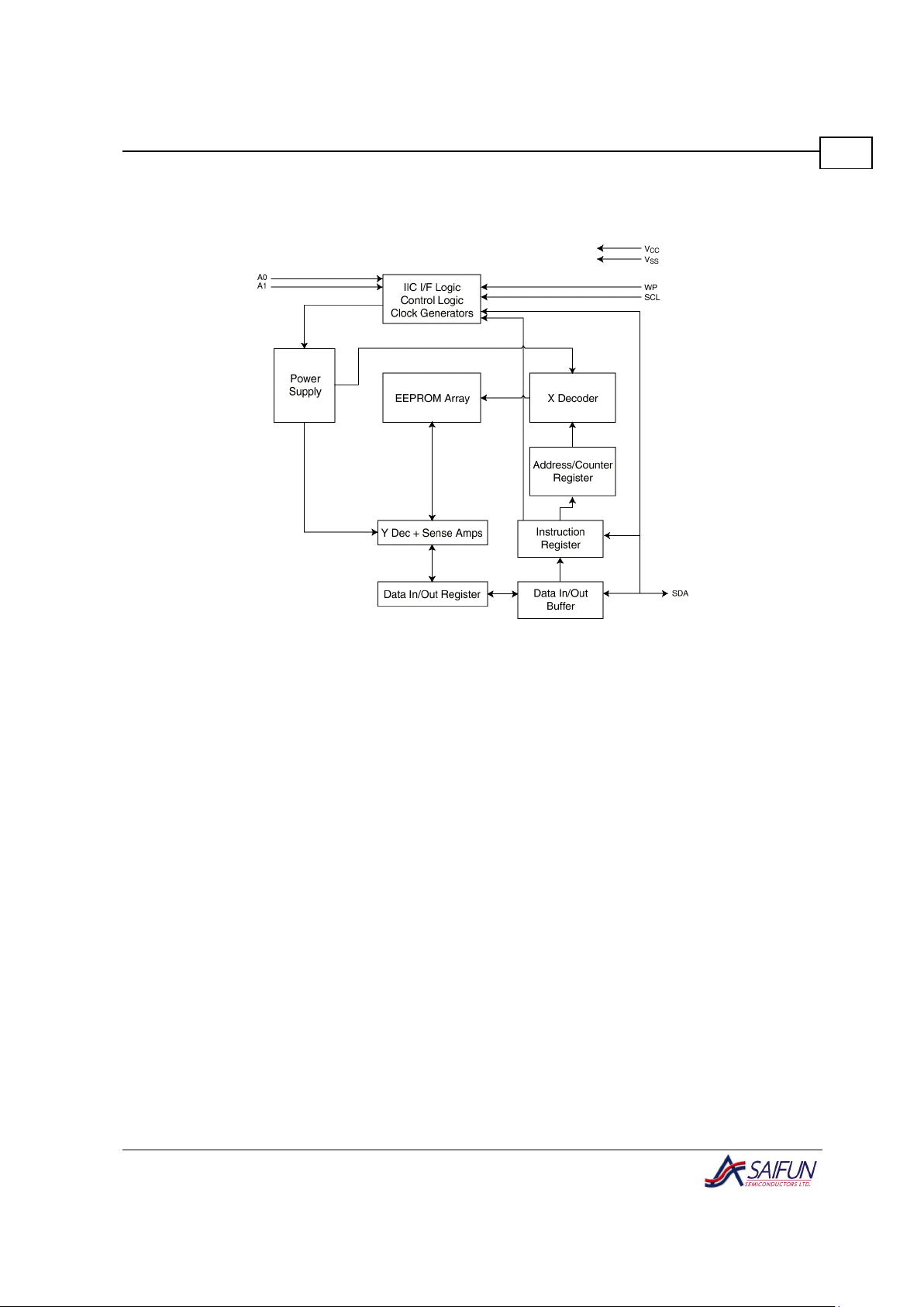
Block Diagram
Figure 1. SA24C1024 Block Diagram
Page 5
SA24C1024 Datasheet
SAIFUN
5
Connection Diagrams
SA24C1024
1
2
3
4
8
7
6
5
NC
A1
NC
V
SS
V
CC
WP
SCL
SDA
SA24C1024
1
2
3
4
8
7
6
5
NC
A1
NC
V
SS
V
CC
SCL
SDA
Figure 2. SO Package (MW), Dual Inline (N) – Top
View
Figure 3. Leadless Package (MLF) – Top View
Note:
For more details, refer to package number N08E and M08D.
Table 1. Pin Names
Symbol
Pin Name Description
NC Not Connected
A1
Device Select Address Input
Pin
Has an internal "weak" pulldown, and assumes logic LOW
when left unconnected.
NC Not Connected
VSS Device Ground Input Pin
SDA IIC Data Input/Output Pin Open Collector/Drain type.
SCL IIC Clock Input Pin
WP
Write Protect
Has an internal "weak" pulldown, and assumes logic LOW
when left unconnected.
When LOW, writing is allowed to the memory array.
When HIGH, writing is not allowed to the memory array, as
defined in Write Protect (WP), page 14.
VCC Device Power Input Pin 2.7 V to 3.6 V
Note:
No A2 or A0 pins (Pins 2 and 3) are provided, and are instead treated as Not
Connected. Internal address comparison assumes pin A2 to be 0, and so the
command code should have its corresponding A2 bit set to 0 as well. The
command code should also have its corresponding A0 bit set to add16 (MSB
address bit).
Page 6
SA24C1024 Datasheet
SAIFUN
6
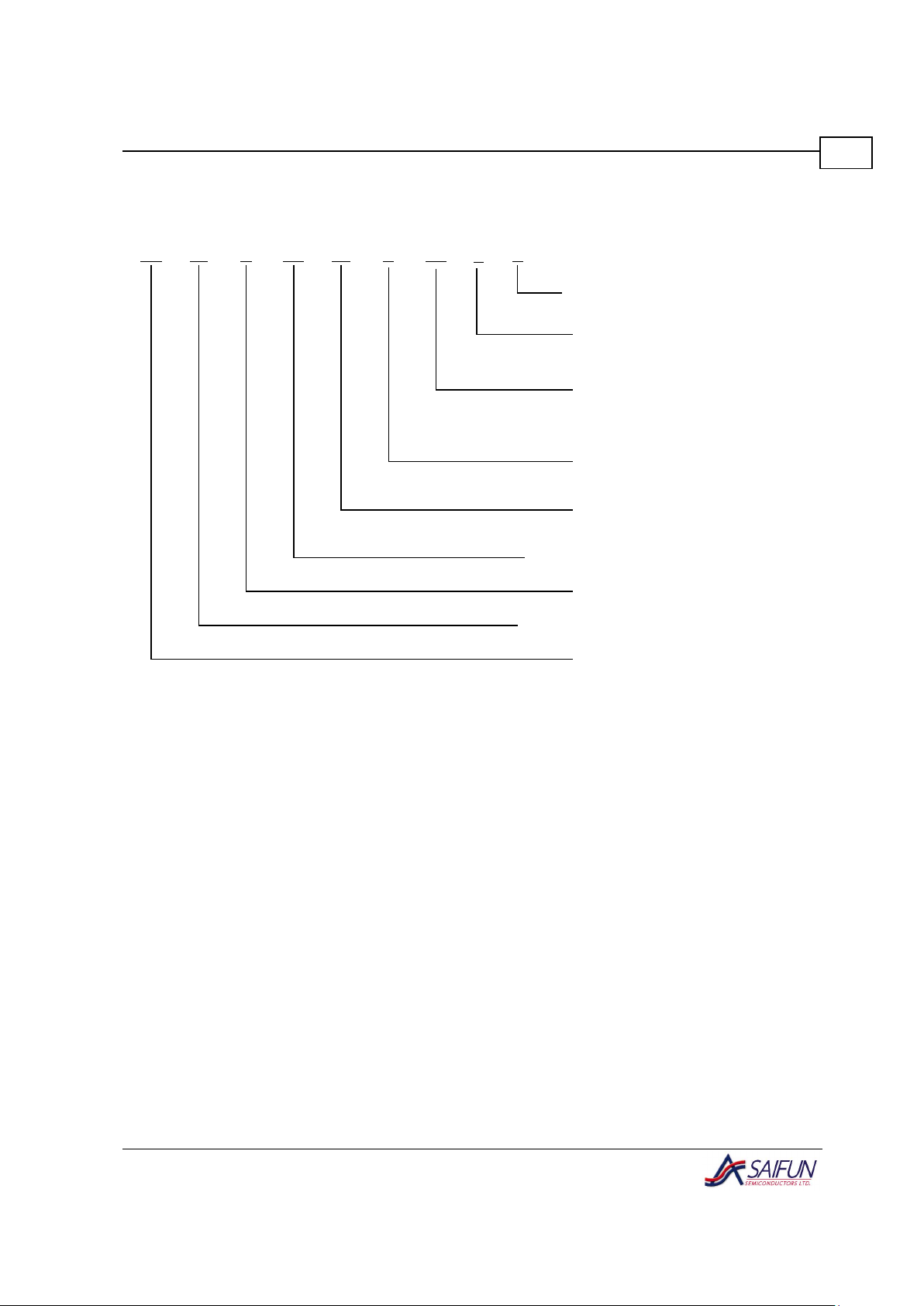
Ordering Information
LZXXC24SA Letter
L
LZ
1024
C
24
SA
Interface
Density
Voltage Operating Range
Description
2.7 V to 3.6 V
2.7 V to 3.6 V
< 0.7 µA Standby Current
1 Mb with Write Protect
CMOS EEPROM
Technology
IIC - 2 Wire
Saifun Non-Volatile
Memory
X
Blank
X
Tube
Tape and Reel
PP
Package
N
MW
MF
8-pin DIP
8-pin SOIC (200 mil)
8-lead MLF
F
Blank
F
Non-lead Free
Lead-free Leads
E
Blank
E
Temp. Range
0 to 70 C
-40 to +85 C
o
o
Figure 4. SA24C1024 Ordering Information
Page 7

SA24C1024 Datasheet
SAIFUN
7
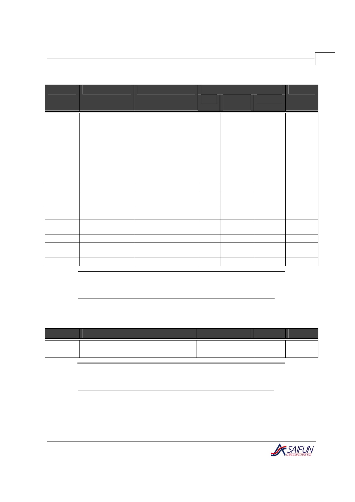
Product Specifications
Absolute Maximum Ratings Operating Conditions
Ambient Storage Temperature
–65 °C to +150 °C
All Input or Output Voltages with
Respect to Ground
4.5 V to -0.3 V
Lead Temperature
(Soldering, 10 seconds)
+300 °C
ESD Rating 2000 V min.
ESD/Latch up Specification (JEDEC 8 Spec)
Human Body Model Minimum 2 KV
Machine Model Minimum 500 V
Latch up
100 mA on all pins, +125 °C
Operating Conditions
Ambient Operating Temperature:
•= SA24C1024
•= SA24C1024E
0°C to +70°C
–40°C to +85°C
Positive Power Supply:
•= SA24C1024
•= SA24C1024LZ
2.7 V to 3.6 V
2.7 V to 3.6 V
Page 8
SA24C1024 Datasheet
SAIFUN
8
VCC (2.7 V to 3.6 V) DC Electrical Characteristics
Limits Symbol Parameter Test Conditions
Min Typ
(Notes)
Max
Units
f
SCL
= 100 kHz (Read) 2 3 mA
f
SCL
= 100 kHz (Write) 8 11 mA
f
SCL
= 400 KHZ (Read) 2 3 mA
f
SCL
= 400 kHz (Write) 8 11 mA
f
SCL
= 1.7 MHz (Read) 5 7 mA
f
SCL
= 1.7 MHz (Write) 8 11 mA
f
SCL
= 3.4 MHz (Read)
5 7 mA
I
CCA
Active Power Supply
Current
f
SCL
= 3.4 MHz (Write)
8 11 mA
ISB Standby Current (L) VIN = GND or V
CC
0.5 1
µA
Standby Current
(LZ)
VIN = GND or VCC 0.2 0.7
µA=
IIL Input Leakage
Current
VIN = GND to V
CC
0.1 1
µA
IOL Output Leakage
Current
V
OUT
= GND to V
CC
0.1 1
µA
VIL Input Low Voltage
-0.3 VCC x 0.3 V
V
IH
Input High Voltage
VCC *
0.7
V
CC
+ 0.5 V
V
OL
Output Low Voltage I
OL
= 3 mA
0.4 V
Notes:
(1) Typical values are TA = +25 °C and nominal supply voltage of 3 V.
(2) Write frequency is 50 Hz.
Capacitance
T
A
= +25 °C, f = 100/400 kHz/1.7 MHz/3.4 MHz, V
CC
= 3V (see note 2)
Symbol Test Conditions Max Units
C
I/O
Input/Output Capacitance (SDA) V
I/O
= 0 V 8 pF
CIN Input Capacitance (A0, A1, A2, SCL) V
IN
= 0 V 6 pF
Notes:
(1) This parameter is periodically sampled and not 100% tested.
(2) Typical values are T
A
= +25 °C and nominal supply voltage of 3 V.
Page 9
SA24C1024 Datasheet
SAIFUN
9
AC Test Conditions
Input Pulse Levels VCC * 0.1 to VCC * 0.9
Input Rise and Fall
Times
10 ns
Input & Output Timing
Levels
VCC * 0.3 to VCC * 0.7
Output Load
1 TTL Gate and CL = 100
pF
AC Testing Input/Output Waveforms
Figure 5. AC Testing Input/Output Waveforms
AC Characteristics (VCC 2.7 V – 3.6 V)
100 kHz 400 kHz 1.7 MHz 3.4 MHz
Symbol Parameter
Min Max Min Max Min Max Min Max
Units
f
SCL
SCL Clock
Frequency
100
400
1700 3400
kHz
t
LOW
Clock Low Period 4700 1300 320 160 ns
t
HIGH
Clock High Period 4000 600 120 60 ns
tSU:STA
Start Condition
Setup Time (for a
repeated START
condition)
4700 600
160 160
ns
t
HD:STA
Start Condition
Hold Time (for a
repeated START
condition)
4000 600
160 160
ns
t
SU:STO
Stop Condition
Setup Time
4000 600
160 160
ns
t
RDA
SDA Rise Time
(depend on
external pullup)
1000 300 20 170 10 85 ns
t
FDA
SDA Fall Time 300 300 20 170 10 85 ns
t
RCL
SCL Rise Time
(depend on
external pullup)
1000 300 20 80 10 40 ns
t
FCL
SCL Fall Time 300 300 20 80 10 40 ns
Page 10

SA24C1024 Datasheet
SAIFUN
10
100 kHz 400 kHz 1.7 MHz 3.4 MHz
Symbol Parameter
Min Max Min Max Min Max Min Max
Units
t
RCL1
SCL Rise Time
(after repeated
START or after
ACK bit)
N/A N/A
N/A
20 160 10 80
ns
t
SU:DAT
Data In Setup Time 250 100 20 20 ns
t
HD:DAT
Data In Hold Time 0 0 0 0 ns
tDH Data Out Hold Time 200 100 0 0 ns
TI
Noise Suppression
Time Constant at
SCL, SDA Inputs
(minimum V
IN
pulse
width)
50 50 10 10 ns
tAA
SCL Low to SDA
Data Out Valid
3001 3500 1001
900
0 170 0 85
ns
t
BUF
Time the Bus Must
Be Free Before a
New Transmission
Can Start
4700 1300
320 160
ns
tWR Write Cycle Time 10 10 10 10 ms
Endurance 1 Million2 Cycles
1
The minimum value is defined in order to bridge the undefined part between VIH and VIL of the falling edge of SCL. The standard
value is 0 ns.
2
This parameter is not tested but ensured by characterization.
Bus Timing
Figure 6. Bus Timing
Page 11

SA24C1024 Datasheet
SAIFUN
11
Write Cycle Timing
Figure 7. Write Cycle Timing
Note:
The write cycle time (tWR) is the time from a valid STOP condition of a Write
sequence to the end of the internal erase/program cycle.
Typical System Configuration
Figure 8. Typical System Configuration
Note:
Due to the open drain configuration of SDA and SCL, a bus-level pullup resistor
is called for (typical value = 4.7 k
Ω).
Page 12

SA24C1024 Datasheet
SAIFUN
12
Background Information
(IIC Bus)
Extended IIC specification is an extension
of the Standard IIC specification, which
enables addressing of EEPROMs with
more than 15 Kbits of memory on an IIC
bus. The difference between the two
specifications is that the Extended IIC
specification defines two bytes of Array
Address information, while the Standard
IIC specification defines only one. All other
aspects are identical between the two
specifications. Using two bytes of the array
address, one Device/Page Block selection
bit (A1) in the Slave address byte and one
address signal (add16) in the Slave
address, it is possible to address up to 2
Mbits (2
8
• 28 • 2 • 2 • 8 = 2 Mbits) of
memory on an IIC bus.
Note that, due to format difference, it is not
possible to have both peripherals that
follow the Standard IIC specification (for
example, 16Kbit EEPROM) and peripherals
that follow the Extended IIC specification
(for example, 1024Kbit EEPROM) on a
common IIC bus.
The IIC bus allows synchronous
bidirectional communication between a
transmitter and a receiver using a Clock
signal (SCL) and a Data signal (SDA).
Additionally, there is one Address signal
(A1) that collectively serves as "chip select
signal" to a device (for example, EEPROM)
on the bus.
All communication on the IIC bus must be
started with a valid START condition (by
the Master), followed by transmittal (also
by the Master) of byte(s) of information
(Address/Data). For every byte of
information received, the addressed
receiver provides a valid acknowledge
(ACK) pulse to further continue the
communication (unless the receiver intends
to discontinue the communication).
Depending on the direction of transfer
(Write or Read), the receiver can either be
a Slave or the Master. A typical IIC
communication concludes with a STOP
condition by the Master.
Addressing an EEPROM memory location
involves sending a command string with
the following information:
[DEVICE TYPE]—[DEVICE/PAGE BLOCK
SELECTION (including ARRAY MSB
ADDRESS BIT (add16)]—[R/WBIT]—
[ARRAY ADDRESS Byte #1]—[ARRAY
ADDRESS Byte #0]
Slave Address
The Slave address is an 8-bit information
consisting of a Device Type field (4 bits), a
Device/Page Block selection field (3 bits)
and one Read/Write bit.
10100A1Add16R/W(LSB)
Device Type
Identifier
Device/ Page
Block Select ion
Figure 9. Slave Address
Page 13

SA24C1024 Datasheet
SAIFUN
13
Device Type
The IIC bus is designed to support a
variety of devices, such as RAMs,
EPROMs, and so on, as well as
EEPROMS. In order to properly identify the
various devices on the IIC bus, a 4-bit
Device Type identifier string is used. For
EEPROMS, this 4-bit string is 1-0-1-0.
Every IIC device on the bus internally
compares this 4-bit string to its own Device
Type string to ensure proper device
selection.
Device/Page Block Selection
When multiple devices of the same type
(for example, multiple EEPROMS) are
present on the IIC bus, the A1 address
information bit is used in device selection.
Every IIC device on the bus internally
compares the first 2 bits of the
Device/Page Block selection string to its
own physical configuration (0, A1pin – for
the SA24C1024, the Device/Page Block
selection MSB is always 0) to ensure
proper device selection. This comparison is
carried out in addition to the Device Type
comparison.
In addition to selecting an EEPROM, the
second and third Device/Page Block
selection bits (A1, add16) can be viewed
as selection controls to a page block within
the selected EEPROM. Each page block is
512 Kbits (64 KBytes) in size.
Read/Write Bit
The last bit of the Slave address indicates
whether the intended access is Read or
Write. If the bit is 1, the access is Read; if it
is 0, the access is Write.
Acknowledge
Acknowledge is an active LOW pulse on
the SDA line that is driven by an addressed
receiver to the addressing transmitter to
indicate receipt of 8 bits of data. The
receiver provides an ACK pulse for every 8
bits of data received. This handshake
mechanism is done as follows:
1. After transmitting 8 bits of data, the
transmitter releases the SDA line
and waits for the ACK pulse.
2. The addressed receiver, if present,
then drives the ACK pulse on the
SDA line during the 9th clock and
releases the SDA line back to the
transmitter.
For more details, see Figure 12.
Array Address#1
This is an 8-bit information that contains
the most significant 8 bits (without the MSB
bit, which is the add16 bit located in the
Slave address byte) of the 17-bit memory
array address.
Array Address#0
This is an 8-bit information that contains
the least significant 8 bits of the 17-bit
memory array address.
Page 14

SA24C1024 Datasheet
SAIFUN
14
Pin Descriptions
Serial Clock (SCL)
The SCL input is used to clock all data into
and out of the device.
Serial Data (SDA)
SDA is a bidirectional pin used to transfer
data into and out of the device. It is an
open drain output and may be wire–ORed
with any number of open drain or open
collector outputs.
Write Protect (WP)
Choice 1: Full Array Write Protect
If pulled HIGH, Write operations are not
executed, and Read operations are
possible. If pulled LOW, normal operation
is enabled, and Read/Write over the entire
memory is possible.
This feature allows the user to assign the
entire memory as ROM, which can then be
protected against accidental programming.
When Write is disabled, the Slave address
and word address are acknowledged but
data is not.
This pin has an internal pulldown circuit.
However, on systems where write
protection is not required, it is
recommended that this pin be tied to V
SS
.
Table 2. Write Protection Truth Table
WP
Pin
"Less Than"
Comparison
T/B Bit
Write
Allowed
1 YES 0 NO
1 NO 0 YES
1 YES 1 YES
1 NO 1 NO
0 Don't Care Don't Care YES
Device Selection Input – A1 (as
Appropriate)
This input serves as a chip select signal to
an EEPROM when multiple EEPROMs are
present on the same IIC bus. These inputs,
if present, should be connected to V
CC
or
V
SS
in a unique manner to enable proper
selection of an EEPROM among multiple
EEPROMs.
During a typical addressing sequence,
every EEPROM on the IIC bus compares
the configuration of these inputs to the
respective two MSBs of the Device/Page
Block selection information (which is part of
the Slave address) to determine a valid
selection. For example, if the two MSB bits
of the Device/Page Block selection are 0-0,
the EEPROM whose Device Selection
input (A1) is connected to the respective
V
SS
is selected.
On the SA24C1024, only A1 is provided,
so the corresponding A2 bit in the
Device/Page Block selection should be set
to 0 during all accesses to the device.
These two pins have a weak internal
pulldown circuit.
Page 15

SA24C1024 Datasheet
SAIFUN
15
Choice 2: Programmable Write Protect
(1)
The Programmable Write protection is available to customers by contacting a Sales
Representative. For this option, use an internal 8-bit wide internal NV-Latch with the following
definition:
T/BA10A11A12A13A14A15A16
Bit 0Bit 1Bit 2Bit 3Bit 4Bit 5Bit 6Bit 7
Address Protection Range - Bit[7:1]
These 7 MSBs of array address determine the
address range that needs to be protected.
Top or Bottom Selection - Bit[0]
0 = Protects from address 0x0000 up to the
address set in Bits[7:1].
1 = Protects from address 1xFFFF up to the
address set in Bits[7:1].
1
Predefined on Sort. Not a user command.
Example
(1024K )
Write Protection
Area
NV-Latch Bit
Setting - Bits [7:0]
Result
1
Full Array
(0x0000 – 0x1FFFF)
0-0-0-0-0-0-0-1
Address bits (A16:A10) issued during the Write
command are compared against bits[7:1] of this
NV-Latch. As bit[0] of this NV-Latch is set to 1, Write
is not allowed as long as the comparison results in a
greater than or equal to status.
2
Bottom Half
(0x0000 – 0x0FFFF)
1-0-0-0-0-0-0-0
As in example 1.
3
Bottom Quadrant
(0x0000 – 0x07FFF)
0-1-0-0-0-0-0-0
As in example 1.
4
Top Quadrant
(0x18000 – 0x1FFFF)
1-1-0-0-0-0-0-1
Address bits (A16:A10) issued during the Write
command are compared against bits[7:1] of this
NV-Latch. As bit[0] of this NV-Latch is set to 1, Write
is allowed as long as the comparison results in a
greater than or equal to status.
5
Top Half
(0x10000 – 0x1FFFF)
1-0-0-0-0-0-0-1
As in example 4.
6 No Write Protection 0-0-0-0-0-0-0-0 As in example 4.
Page 16

SA24C1024 Datasheet
SAIFUN
16
Device Operation
The SA24C1024 supports a bidirectional
bus-oriented protocol, which defines any
device that sends data onto the bus as a
transmitter and the receiving device as the
receiver. The device controlling the transfer
is defined as the Master and the device
that is controlled is the Slave. The Master
always initiates data transfers and provides
the clock for both transmit and receive
operations. The SA24C1024 is therefore
considered to be the Slave in all
applications.
Clock and Data Conventions
Data states on the SDA line can change
only during SCL LOW. SDA state changes
during SCL HIGH are reserved for
indicating START and STOP conditions.
For more details, see Figure 10.
START Condition
All commands are preceded by the START
condition, which is a HIGH-to-LOW
transition of SDA when SCL is HIGH. The
SA24C1024 continuously monitors the
SDA and SCL lines for the START
condition and does not respond to any
command until this condition has been met.
For more details, see Figure 11.
STOP Condition
All communications are terminated by a
STOP condition, which is a LOW-to-HIGH
transition of SDA when SCL is HIGH. The
STOP condition is also used by the
SA24C1024 to place the device in the
standby power mode. For more details, see
Figure 11.
SA24C1024 Array Addressing
During Read/Write operations, addressing
the EEPROM memory array involves
providing the Slave address with the Most
Significant Address bit (add16), as well as
two address bytes, Word Address 1 and
Word Address 0. The Word Address 1 byte
contains the 8 MSBs of the array address,
while the Word Address 0 byte contains
the 8 LSBs of the array address.
Page 17

SA24C1024 Datasheet
SAIFUN
17
Figure 10. Data Validity
Figure 11. START and STOP Definition
Figure 12. Acknowledge Response from Receiver
Page 18

SA24C1024 Datasheet
SAIFUN
18
Write Operations
Byte Write
Two address bytes are required after the
Slave address, which contains the Most
Significant Address bit (add16), for a byte
Write operation. These 17 address bits
select one out of the 128K locations in the
memory. The Master provides these
address bytes, and for each address byte
received, the SA24C1024 responds with an
ACK pulse. The Master then provides a
byte of data to be written into the memory.
Upon receipt of this data, the SA24C1024
again responds with an ACK pulse. The
Master then terminates the transfer by
generating a STOP condition, at which
time the SA24C1024 begins the internal
write cycle to the memory. While the
internal write cycle is in progress, the
SA24C1024 inputs are disabled, and the
device does not respond to any requests
from the Master for the duration of t
WR
. For
more details regarding the address,
acknowledge and data transfer sequence,
see Figure 13.
Page Write
To minimize write cycle time, the
SA24C1024 offers a Page Write feature,
which allows simultaneous programming of
up to 128 contiguous bytes. To facilitate
this feature, the memory array is organized
in terms of “pages.” A page consists of 128
contiguous byte locations starting at every
128-byte address boundary (for example,
starting at array address 0x00000,
0x00080, 0x00100, and so on).
The Page Write operation is confined to a
single page, which means that it does not
cross over to locations on the next page
but rolls over to the beginning of the page
whenever the end of the page is reached
and additional data bytes continue to be
provided. A Page Write operation can be
initiated to begin at any location within a
page (the starting address of the Page
Write operation does not have to be the
starting address of a page).
Page Write is initiated in the same manner
as the Byte Write operation; however,
rather than terminate the cycle after
transmitting the first data byte, the Master
can further transmit up to 127 more bytes.
After the receipt of each byte, the
SA24C1024 responds with an ACK pulse,
increments the internal address counter to
the next address, and is ready to accept
the next data. If the Master transmits more
than 128 bytes prior to generating the
STOP condition, the address counter rolls
over and previously loaded data is
re-loaded. As with the Byte Write
operation, all inputs are disabled until
completion of the internal write cycle. For
more details regarding the address,
acknowledge, and data transfer sequence,
see Figure 14.
Page 19

SA24C1024 Datasheet
SAIFUN
19
Acknowledge Polling
Once the STOP condition is issued to
indicate the end of the host’s Write
operation, the SA24C1024 initiates the
internal write cycle. ACK polling can be
initiated immediately, which involves
issuing the START condition followed by
the Slave address for a Write operation.
If the SA24C1024 is still busy with the
Write operation, no ACK is returned. If the
SA24C1024 has completed the Write
operation, an ACK is returned and the host
can then proceed with the next Read or
Write operation.
Write Protection
Programming of the memory does not take
place if the SA24C1024's WP pin is pulled
HIGH. The SA24C1024 responds to Slave
and byte addresses but does not generate
an ACK after the first byte of data has been
received. This means that the program
cycle is not started when the STOP
condition is asserted.
1010 0100
A
1
A
d
d
16
A
C
K
A
C
K
A
C
K
S
T
A
R
T
S
T
O
P
SLAVE
ADDRESS
WORD
ADDRESS
DATA
Bus Activity:
Master
SDA Line
Bus Activity:
EEPROM
Figure 13. Byte Write
1010 0100
A1A
d
d
16
A
C
K
A
C
K
A
C
K
S
T
A
R
T
S
T
O
P
SLAVE
ADDRESS
WORD
ADDRESS (n)
DATA n
Bus Activity:
Master
SDA Line
Bus Activity:
EEPROM
A
C
K
DATA n + 1
A
C
K
DATA n + 15
Figure 14. Page Write
Page 20

SA24C1024 Datasheet
SAIFUN
20
Read Operations
Read operations are initiated in the same
manner as Write operations, with the
exception that the R/
W bit of the Slave
address is set to 1. There are three basic
Read operations: current address Read,
random Read, and sequential Read.
Current Address Read
Internally the SA24C1024 contains an
address counter that maintains the address
of the last byte accessed, incremented by
1. Therefore, if the last access (either a
Read or Write) was to address n, the next
Read operation would access data from
address n + 1. Upon receipt of the Slave
address with R/
W set to 1, the SA24C1024
issues an ACK pulse and transmits the 8bit word. The Master does not
acknowledge the transfer but does
generate a STOP condition, which causes
the SA24C1024 to discontinue
transmission. For more details regarding
the sequence of address, acknowledge
and data transfer, see Figure 15.
Random Read
Random Read operations enable the
Master to access any memory location in a
random manner. Prior to issuing the Slave
address with the R/
W bit set to 1, the
Master must first perform a “dummy” Write
operation. The Master issues the START
condition, the Slave address's R/
W bit is
set to 0 and the byte address is read. After
the byte address is acknowledged, the
Master immediately issues another START
condition and the Slave address's R/
W bit
is set to 1. This is followed by an ACK from
the SA24C1024 and then by the 8-bit word.
The Master does not acknowledge the
transfer but does generate the STOP
condition, which causes the SA24C1024 to
discontinue transmission. For more details
regarding address, acknowledge, and data
transfer sequence, see Figure 16.
Sequential Read
Sequential Reads can be initiated as either
a current address Read or random access
Read. The first word is transmitted in the
same manner as the other Read modes;
however, the Master responds with an ACK
pulse, indicating it requires additional data.
The SA24C1024 continues to output data
for each ACK received. The Read
operation is terminated either by the
Master not responding with an ACK pulse
or by generating a STOP condition.
Page 21

SA24C1024 Datasheet
SAIFUN
21
The data output is sequential, with the data
from address n followed by the data from
n + 1. The address counter for Read
operations increments all word address
bits, enabling the entire memory contents
to be serially read during one operation.
After the entire memory has been read, the
counter rolls over to the beginning of the
memory. The SA24C1024 continues to
output data for each ACK received. For
details regarding the address,
acknowledge, and data transfer sequence,
see Figure 17.
1010 00 1
A1A
d
d
16
A
C
K
S
T
A
R
T
S
T
O
P
SLAVE
ADDRESS
DATA
Bus Activity:
Master
SDA Line
Bus Activity:
EEPROM
NO
A
C
K
Figure 15. Current Address Read
1010 0 0
A1A
d
d
16
A
C
K
A
C
K
A
C
K
S
T
A
R
T
S
T
O
P
SLAVE
ADDRESS
WORD
ADDRESS
Bus Activity:
Master
SDA Line
Bus Activity:
EEPROM
NO
A
C
K
S
T
A
R
T
SLAVE
ADDRESS
DATA n
Figure 16. Random Read
1
A
1
A
d
d
16
A
C
K
A
C
K
S
T
O
P
SLAVE
ADDRESS
DATA n + 1
Bus Activity:
Master
SDA Line
Bus Activity:
EEPROM
NO
A
C
K
DATA n + 1
A
C
K
DATA n + 2
A
C
K
DATA n + x
Figure 17. Sequential Read
Page 22

SA24C1024 Datasheet
SAIFUN
22
Switching from
Standard/Fast Modes to
High-speed Mode and
Back
The Standard (S), Fast (F) and High-speed
(HS) modes are defined according to the
IIC Bus specifications as follows:
•= S mode: Maximum bit transfer
rates of 100 Kbps.
•= F mode: Maximum bit transfer
rates of 400 Kbps.
•= HS mode: Maximum bit transfer
rates of 3.4 Mbps.
After reset and initialization, the device
must be put in F mode. The Master on the
bus can then choose to switch the
connected Slave devices to HS mode. The
Slave device must recognize the
"S 00001XXX A" sequence and then must
switch its internal circuit from F mode to
HS mode. Each device must also
recognize the STOP condition and switch
back to F mode.
Timings and flow can be seen in Figure 18
and Figure 19.
Figure 18. Data Transfer
Page 23

SA24C1024 Datasheet
SAIFUN
23
Figure 19. A Complete HS Mode Transfer
Page 24

SA24C1024 Datasheet
SAIFUN
24
Physical Dimensions
All measurements are in inches (millimeters), unless otherwise specified.
Figure 20. 8-pin Molded Small Outline Package (MW8), Package Number M08D
Page 25

SA24C1024 Datasheet
SAIFUN
25
Figure 21. Molded Dual-in-Line Package (N), Package Number N08E
Page 26

SA24C1024 Datasheet
SAIFUN
26
Figure 22. 8-pin MLF Leadless Package
Page 27

SA24C1024 Datasheet
SAIFUN
27
Contact Information
International Headquarters United States
Saifun Semiconductors Ltd.
ELROD Building
45 Hamelach St.
Sappir Industrial Park
Netanya 42504
Israel
Tel.: +972-9-892-8444
Fax: +972-9-892-8445
Saifun Semiconductors Inc.
2350 Mission College Blvd.
Suite 1070
Santa Clara, CA 95054
U.S.A.
Tel: +1-408-982-5888
Fax: +1-408-982-5890
Email: tech_support@saifun.com
http://www.saifun.com
Revision History
Rev Date Description of Change
0.0 05-Sep-02 Initial release
1.0 05-Dec-02 Editing and review
1.1 26-Aug-03 Endurance, MLF Package and tDH
© Saifun Semiconductors Ltd. 2003
Saifun reserves the right, without notice, to change any of the products described in this guide, in order to improve functionality,
reliability or design. Saifun assumes no liability arising from the application or use of any product described in this guide; and
under its patent rights, gives no authorization for the use of this product or associated products. Saifun makes no warranty for use
of its products, other than expressly provided by Saifun in any applicable warranty. The Buyer will not hold Saifun responsible for
direct or indirect damages and expenses, as well as any claim of injury or death, associated with the unauthorized use, including
claims of manufacture or design negligence.
Saifun and Saifun NROM are trademarks or registered trademarks of Saifun Semiconductors Ltd. Other company and brand
products and service names are trademarks or registered trademarks of their respective holders.
Life Support Policy
Saifun's products are not authorized for use as critical components in life support devices or systems without the express written
approval of the President of Saifun Semiconductors Ltd. As used herein:
1. Life support devices or systems are devices or
systems which, (a) are intended for surgical
implant into the body, or (b) support or sustain
life, and whose failure to perform, when properly
used in accordance with instructions for use
provided in the labeling, can be reasonably
expected to result in a significant injury to the
user.
2. A critical component is any component of a life
support device or system whose failure to
perform can be reasonably expected to cause the
failure of the life support device or system, or to
affect its safety or effectiveness.
 Loading...