

Page 1

sames
FEATURES
SA2030
SA2030
PCM FRAME ALIGNER
n Frame Alignment Recovery and loss
in accordance with CCITT
recommendations G.732 and G.737
n Jitter and phase-wander immunity
exceed the requirements of CCITT
recommendation G.823.
n Internal 1½ frame elastic buffer.
n Detection of incoming Alarm-
Indication of Slip, loss of frame
n
synchronisation, and loss of route clock
conditions.
n ISO-CMOS technology, TTL
Compatible.
n Pin-for-Pin replacement for Siemens
PEB 2030 and SM 300
n Microprocessor Interface
Indication-Signal (AIS), and Distant
Alarm
APPLICATIONS
n Delay compensation and clock
alignment between 2,048MHz PCM30 transmission lines, and terminating
equipment.
n Control of Jitter and Wander within
Digital Networks.
n Delay compensation between switching
stages.
n Interfacing of PCM systems operating
with different clocks.
n PCM concentrators and subscriber
multiplexers.
GENERAL DESCRIPTION
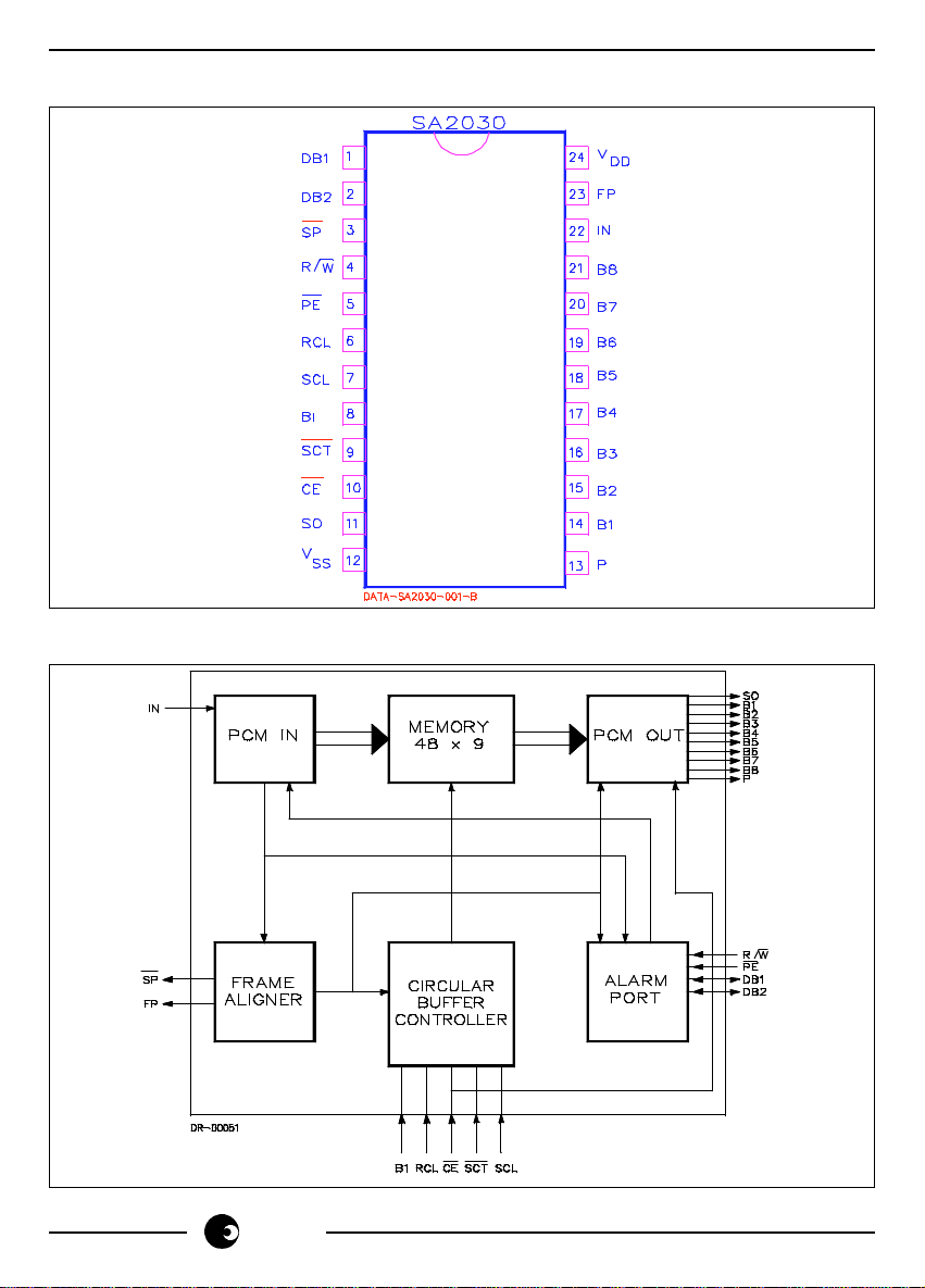
The SA2030 is designed to interface PCM-30 routes with switching systems. The device
synchronises with the frame-format of the incoming data, and outputs this data in
accordance with the bit and frame timing of the terminating equipment. The circuit is
designed to tolerate delay, drift, wander and jitter of the incoming data and clock, and thus
simplifies the design of data- and clock-recovery hardware. The internal 1½ frames
elastic buffer provides for delay compensation and wander immunity. If the bounds of
the buffer are exceeded, the SA2030 will either repeat or drop a frame. The circuit will
accurately detect incoming Alarm-Indication-Signal (AIS) conditions, in accordance with
CCITT recommendation G.737. Loss of frame alignment is indicated on both dedicated
outputs and by outputting of AIS. The circuit includes a bidirectional alarm port for
interrogation of alarm conditions.
1/12
20.01.93
M74-1885
sames
Page 2
SA2030
PIN CONFIGURATION
BLOCK DIAGRAM
2/12
sames
Page 3

SA2030
FUNCTIONAL DESCRIPTION
PCM INPUT AND FRAME-ALIGNMENT
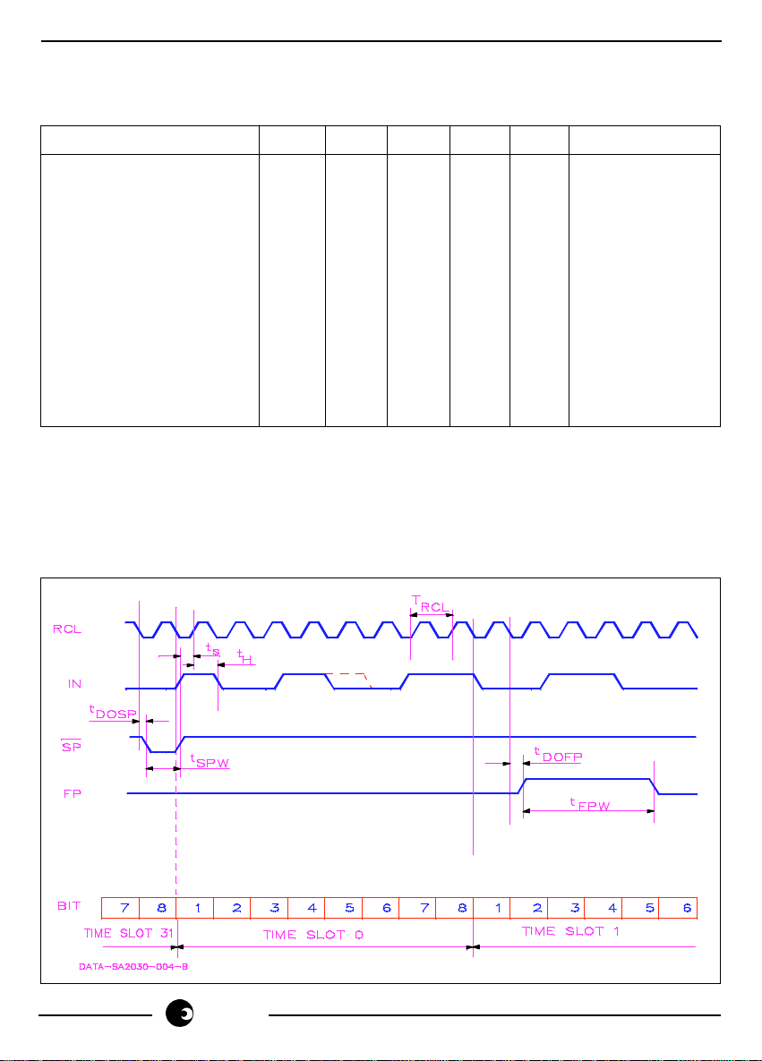
The SA2030 accepts route data on the IN input pin, on rising edges of the route clock RCL.
The circuit synchronises with the frame format of the incoming data by identification of
the Frame Alignment Signal (FAS) and the Service Word (SW) in time slot zero of the
PCM frame. The algorithm used for recovery and loss of frame synchronisation is in
accordance with CCITT recommendation G.737. After the circuit has gained
synchronisation with the incoming PCM-30 data stream, it outputs a synchronisation
pulse SP on alternate frames, during the bit interval prior to time-slot-zero of frames
containing the FAS word. The circuit will output a fault pulse on the FP output every time
errors are detected in the incoming FAS word. When the circuit is unable to synchronise
with the incoming data format, the SA2030 will generate a fault pulse every alternate
frame, and outgoing synchronisation pulses will be suppressed.
PCM OUTPUT
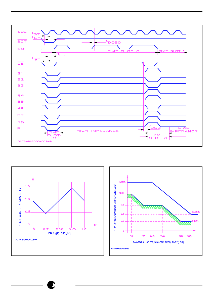
Data is clocked out on falling edges of the System Clock (SCL). PCM output is clocked
out serially on the SO output, and is made available in parallel on a tristate bus with parity
(B1-B8, P). The tristate outputs are enabled by asserting CE. The SA2030 must be
provided with a System Clock Trigger (SCT) pulse to define the required output frame
timing. The SCT pulse defines the bit interval immediately prior to the start of time-slotzero, on every alternate frame. Acceptance of SCT pulses is only enabled when CE is
asserted. The tristate parallel bus, with CE control, simplifies the use of the circuit in
multiplex and switching applications.
ELASTIC BUFFER
Incoming PCM data is saved in dual-ported RAM. The RAM has capacity for 1½ frames
of data. The SA2030 can thus accommodate any required frame delay between the
incoming data timing, and the required output frame timing. When the bounds of the
buffer are exceeded, whole frames are either dropped or repeated. The action of
dropping or repeating a received frame is called slip. Depending on the frame-delay, the
SA2030 can tolerate between ½ and 1½ frame of wander without requiring to alternately
repeat and drop frames. The design of the elastic buffer controller provides for correct
performance under severe clock-and-data-jitter conditions. The SA2030 exceeds the
requirements of CCITT recommendation G.823, and can be used to control jitter and
wander within digital networks. The 1½ frame buffer is enabled by setting BI = 0. If BI
= 1, the buffer length is limited to only one frame. The frame delay through the framealigner is then constrained to be less than one frame. The buffer inhibit mode is useful
for delay compensation within a switching system, where drift and wander do not occur.
sames
3/12
Page 4

SA2030
ALARM SUBSYSTEM
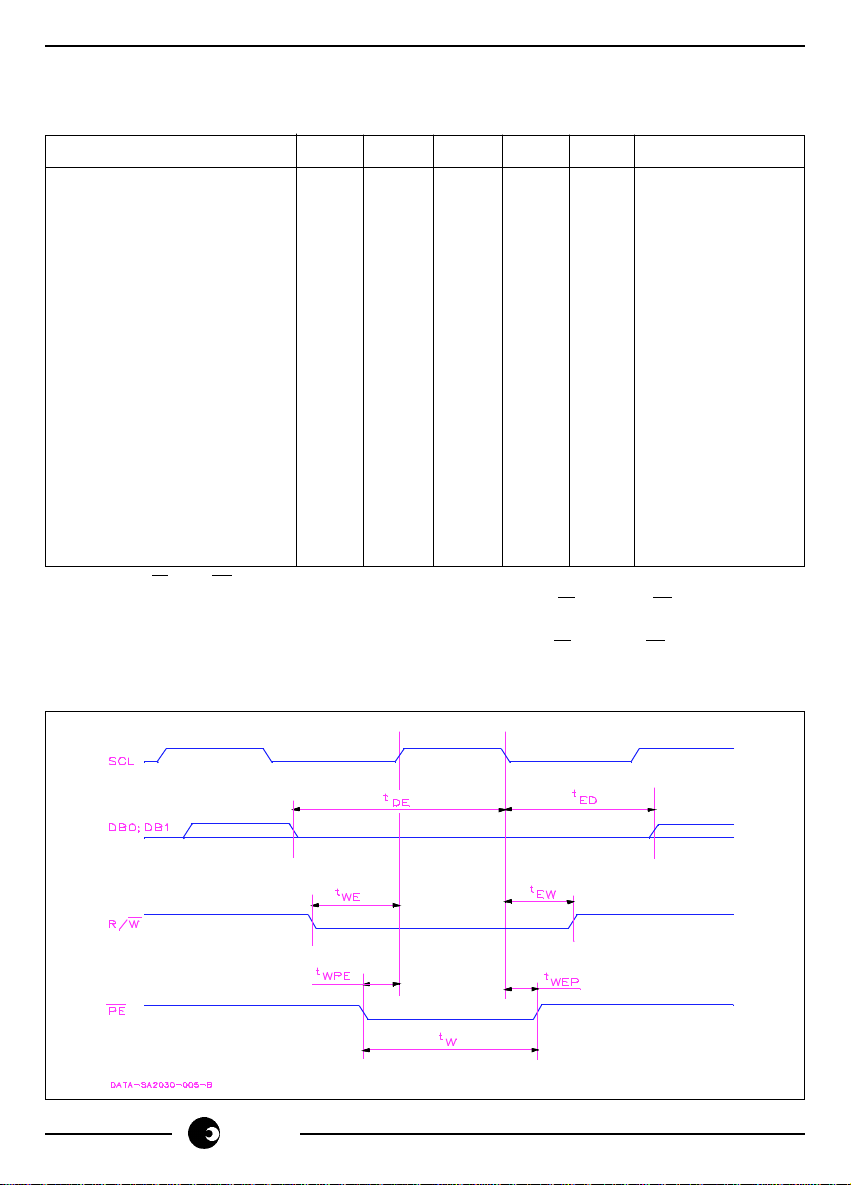
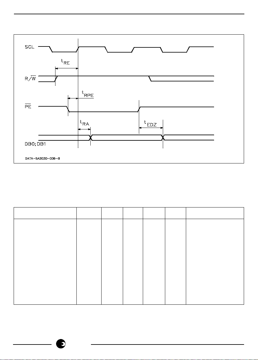
The alarm system may be used by the host equipment to determine the operation status
of the SA2030. The SA2030 provides a bidirectional alarm-port interface DB1 and DB2.
The direction of the interface is controlled by the R/W line. Transfers to or from the
interface are enabled by strobing the port-enable (PE) input. The circuit includes two 2bit alarm registers. The four flags in these registers are set when:
- Incoming Alarm-Indication-Signal is received (AIS)
- Loss of frame synchronisation occurs (SYLOSS)
- A distant alarm is received (DISAL)
- A frame slip occurs (SLIP)
* The algorithm used for detection of incoming AIS is in accordance with CCITT
recommendation G.737. That is, AIS will be correctly detected, even in the presence
of random errors, at a rate of 1 in 103.
* The loss of frame synchronisation flag is set if loss of frame-alignment occurs, if the
route clock is missing or too slow, or if a system-clock-trigger (SCT) pulse is not
applied to the circuit once every alternate frame.
* The distant alarm flag is set if bit 3 of time-slot-zero of frames not containing FAS
is true.
* The frame-slip is set if the frame aligner either drops or repeats a frame.
Selection of which of the two alarm registers is to be read, is carried out by first writing
a command to the comand register via DB1 and DB2. Four commands are supported:
- Enable Read of Alarm Group 1
- Enable Read of Alarm Group 2
- Clear all alarm flags
- Simulate Alarms
Alarm Group 1 includes the AIS and frame synchronisation flags. Alarm Group 2 includes
the Slip and distant alarm flags.
Once an alarm flag is set, it can only be cleared by writing the "clear-all-alarms" command
to the alarm command register. That is, these flags remain set until explicitly cleared.
The simulate-alarm command provides an alarm system self-test capability. This
command simulates all alarm conditions at their sources. If the circuit is operating
correctly, all alarm flags should be set after issuing this command. Alarm simulation tests
the loss of synchronisation function of the frame alignment state-machine, and the AIS
detection logic, and thus may require up to four-frames to complete. After all of the alarm
flags are set, alarm simulation is disabled, and the circuit reverts to normal operation.
4/12
sames
Page 5
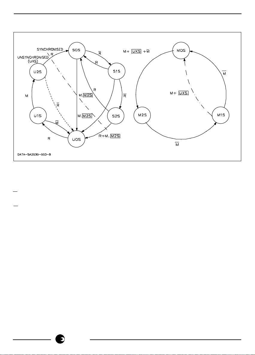
LOSS AND RECOVERY OF FRAME ALIGNMENT
CONDITIONS
R - Good FAS Received
R - One or more errors in FAS
M - Bit 2 of service word = 1 (Good SW)
M - Bit 2 of service word = 0 (Bad SW)
UXS - Unsynchronised stated U0S, U1S or U2S
M2S - Two service word errors received state
SA2030
STATES
U0S - Unsynchronised, zero frames OK state
U1S - Unsynchronised, one frame OK state
U2S - Unsynchronised, two frame OK state
S0S - Synchronised, zero FAS errors state
S1S - Synchronised, one FAS error state
S2S - Synchronised, two FAS errors state
M0S - Zero service word errors state
M1S - One service word error state
M2S - Two service word errors state
sames
5/12
Page 6

SA2030
Command
Mnemonic
Write Alarms Read
Description
DB2 DB1 DB2 DB1
RAG1 0 0 AIS SYLOSS Read Alarm Group 1
RAG2 0 1 SLIP DISAL Read Alarm Group 2
CLR 1 0 - - Alarm Register Clear
SIM 1 1 - - Simulate Alarms
Notes: 1. After the CLR or SIM commands, neither RAG1 or RAG2 are selected
for reading. Thus subsequent reading will return undefined data.
2. Allow 4 frames for the SIM command to execute before issuing a RAG1
or RAG2 command.
6/12
sames
Page 7
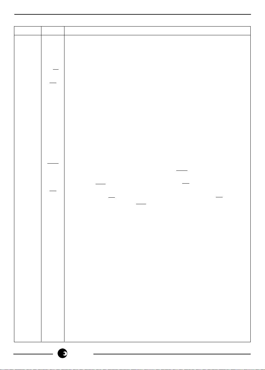
PIN DESCRIPTION
Pin No. Name Function
1 DB1 Bidirectional Alarm Port
2 DB2 Bidirectional Alarm Port
3 SP Synchronisation Pulse output. Asserted during the bit interval immediately
prior to time-slot-zero of frames that contain FAS. Suppressed in the event
of frame-alignment loss.
4 R/W Input for controlling direction of Alarm port data bus DB1 and DB2.
Internally pulled up to V
5 PE Alarm port enable. Asserting this pin enables data transfers to or from
DB1 and DB2. Internally pulled up to V
6 RCL Route Clock Input. 2.048 MHz clock that defines PCM input data timing.
The route clock is usually extracted from the route data.
7 SCL System Clock Input. 2.048 MHz clock that defines the timing of the
terminating equipment.
8 BI Buffer Inhibit Input. When true, the 1½ frame buffer is inhibited, and the
output frame timing is constrained to be within one-frame of the input
frame timing. When false, the full 1½ frame buffer is enabled, and
immunity to wander is maximised. Buffer Inhibit Mode of operation is
intended for delay compensation between switching stages in one exhange
system. Internally pulled up to VDD.
9 SCT Station Clock Trigger input. Low going pulse used by the host system to
define the required output frame timing. SCT should be asserted on
alternate frames, during the data-bit interval immediately prior to timeslot-zero. SCT input is enabled by asserting CE.
10 CE Chip Enable input. When asserted the parallel outputs, B1 to B8 and P
are enabled. When CE = 1, parallel outputs are high impedance. CE must
also be asserted to enable the SCT input. Internally pulled-up to V
11 SO Serial PCM Data Output. PCM-30 format output of aligned and retimed
data. Data clocked out under control of the System Clock SCL.
12 V
13 P Parity Bit 3-state Ouput. Parity check for internal RAM. RAM data is saved
Ground (0V) supply.
SS
with Parity bit. Even Parity is used.
14 B1 3-State PCM Parallel Output (PCM sign bit).
15 B2 3-State PCM Parallel Output
16 B3 3-State PCM Parallel Output
17 B4 3-State PCM Parallel Output
18 B5 3-State PCM Parallel Output
19 B6 3-State PCM Parallel Output
20 B7 3-State PCM Parallel Output
21 B8 3-State PCM Parallel Output (LSB)
22 IN PCM data input. Data is derived from route data and is clocked into the
circuit on rising edges of RCL.
23 FP Fault Pulse Output. Fault pulses of 4 Route Clock cycles duration are
delivered whenever errors are detected in FAS, or on alternate frames in
the event of Frame Alignment loss.
24 V
Supply Voltage (+5V Nominal)
DD
.
DD
.
DD
SA2030
.
DD
sames
7/12
Page 8
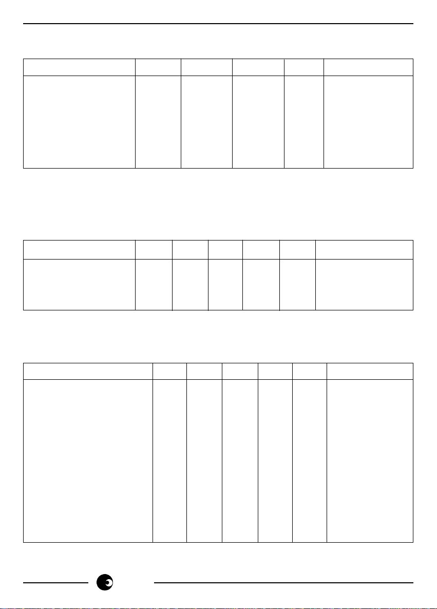
SA2030
Absolute Maximum Ratings
Characteristics Sym Min Max Unit Conditions
Supply Voltage V
Voltage on any pin V
Storage Temperature T
Total power dissipation P
Operating ambient T
DD
PIN
STG
TOT
OP
-0,3 7,0 V -
VSS -0,3 VDD +0,3 V -
-55 125 °C -
- 100 mW 25°C
070°C-
temperature range
Stresses beyond these limits may cause permanent damage to the device. Exposure to
absolute maximum ratings for extended periods may affect device reliability.
Recommended Operating Conditions
Characteristics Sym Min T yp Max Unit Conditions
Supply voltage V
Voltage on any pin V
Operating temperature T
4,75 5,00 5,25 V -
DD
PIN
OP
V
SS
02570°C -
-VDDV-
Electrical Characteristics
T
= 25°C, over recommended operating supply voltage range.
AMB
Characteristics Sym Min Ty p Max Unit Test Conditions
Standby Power Consumption P
Power Consumption P
Input High Voltage V
Input Low Voltage V
Input Pull-up Current I
Output High Voltage V
Output Low Voltage V
High Impedance Leakage
Current I
STBY
OPER
IH
IL
PU
OH
OL
OZ
- - 1, 0 m W Outputs, Unloaded,
= 5V
V
DD
- 25,0 - m W Outputs Unloaded,
at 2,048MHz,
= 5V
V
DD
2,4 - V
- - 0,8 V
-150 -5 µA V
IN
= 0V
2,7 - - V IOH = -1,0mA
- - 0,4 V IOL = 1,0mA
-50-nA
8/12
sames
Page 9
SA2030
Route Subsystem Timing
(At VDD = 5V, T
= 25°C)
AMB
Characteristics Sym Min Ty p Max Unit Test Conditions
Route Clock Period T
Route Clock Duty Cycle D
Input Data Setup time t
Input Data Hold time t
Synch Pulse Width t
Synch Pulse Delay t
Fault Pulse Width t
Fault Pulse Delay t
SPW
DOSP
FPW
DOFP
Synch Pulse Repeat Period T
Fault Pulse Repeat Period T
Note: 1. The CCITT recommends clock frequency of 2,048MHz ±50ppm.
2. Incorrect Slip operation may occur if the Route clock and System clock differ by
more than 1% (10000ppm).
3. A Synch Alarm will be issued if the Route Clock frequency is less than 75% of the
Station Clock frequency.
400 488 600 ns Note 1, 2, 3
RCL
RCL
25 50 75 % at 2,048MHz
150 - - ns
S
40 - - ns
H
- 488 - ns In Frame Synch
- - 200 ns In Frame Synch
- 1952 - ns After Bad FAS
- - 200 ns After Bad FAS
SP
FP
- 250 - µ s In Frame Synch
- 250 - µ s Out of Frame
Synch
Route Subsystem Timing Diagram
sames
9/12
Page 10
SA2030
Alarm Port Read / Write Timing
(At VDD = 5V, T
= 25°C)
AMB
Characteristics Sym Min Ty p Max Unit Test Conditions
Data Setup Time t
Write Enable Setup Time t
100 - - ns
DE
150 - - ns
WE
Port Enable Write Setup
Time t
Data Hold Time t
Write Enable Hold Time t
Port Enable Hold Time t
Write Duration t
Read Enable Setup Time t
150 - - ns
WPE
100 - - ns
ED
100 - - ns
EW
100 - - ns
WEP
444 896 - ns at 2,048MHz
N
150 - - ns
RE
Port Enable Read Setup
Time t
Read Access Time t
High Impedance Delay t
Note: 1. R/W and PE are read on rising edges of SCL.
2. Data is latched on failing edges of SCL subject to R/W = 0, and PE = 0 on
previous SCL rising edge.
3. Data is output after rising edge of SCL subject to R/W = 1 and PE = 0.
150 - - ns
RPE
RA
EDZ
- - 350 ns CL=50pF, RL=5K
- - 160 ns
Alarm Port Write Timing Diagram
10/12
sames
Page 11
Alarm Port Read Timing Diagram
SA2030
Data Output Timing
(at VDD = 5V, T
= 25°C)
AMB
Characteristics Sym Min Typ Max Unit Conditions
System Clock Period t
SCL
400 488 600 ns Note 1
System Clock Duty
Cycle D
SCL
25 50 75 %
Clock Trigger Setup
Time t
ST
150 - - ns
Clock Trigger Hold
Time t
SO Output Delay t
HT
DOSO
100 - - ns
- - 200 ns CL=15pF, RL=10K
BI.. B8, P Output
Delay t
DOB
- - 200 ns CL=15pF, RL=10K
Note: 1 . The CCITT recommends a data rate of 2,048MHz + 50ppm.
sames
11/12
Page 12
SA2030
JITTER IMMUNITY
12/12
FRAME DELAY
sames
 Loading...