

Page 1
INTEGRATED CIRCUITS
SA2410
2.45GHz RF power amplifier and T/R
switch
Preliminary specification 1997 Sep 09
IC17 Data Handbook
Page 2
Philips Semiconductors Preliminary specification
2.45GHz RF power amplifier and T/R switch
DESCRIPTION
The SA2410 is a GaAs monolithic power amplifier with an integrated
T/R switch designed to meet requirements for 802.11 (WLAN). The
SA2410 uses an on–chip 4 GHz oscillator to generate the negative
bias, thus eliminating the need for a negative supply. It operates
from 3V to 5.5V and consumes 125 mA with an output power of 18.5
dB (typ). It is suitable for other 2.45 GHz ISM band applications.
FEATURES
•V
=3V–5.5V
CC
•No negative bias needed
•I
=125mA (typ) @ 3.3V
CC
•P
=18.5 dB(typ)
OUT
•Gain=29dB (typ)
•Attenuation range=16dB (typ)
•LQFP–32 package
APPLICA TIONS
•802.1 1 WLAN
•2.4–2.5 GHz ISM BAND
IM3<–30dBc
IM5<–50dBc
SW
V
GND
V
GND
V
GC1
V
GC2
GND
OUT1
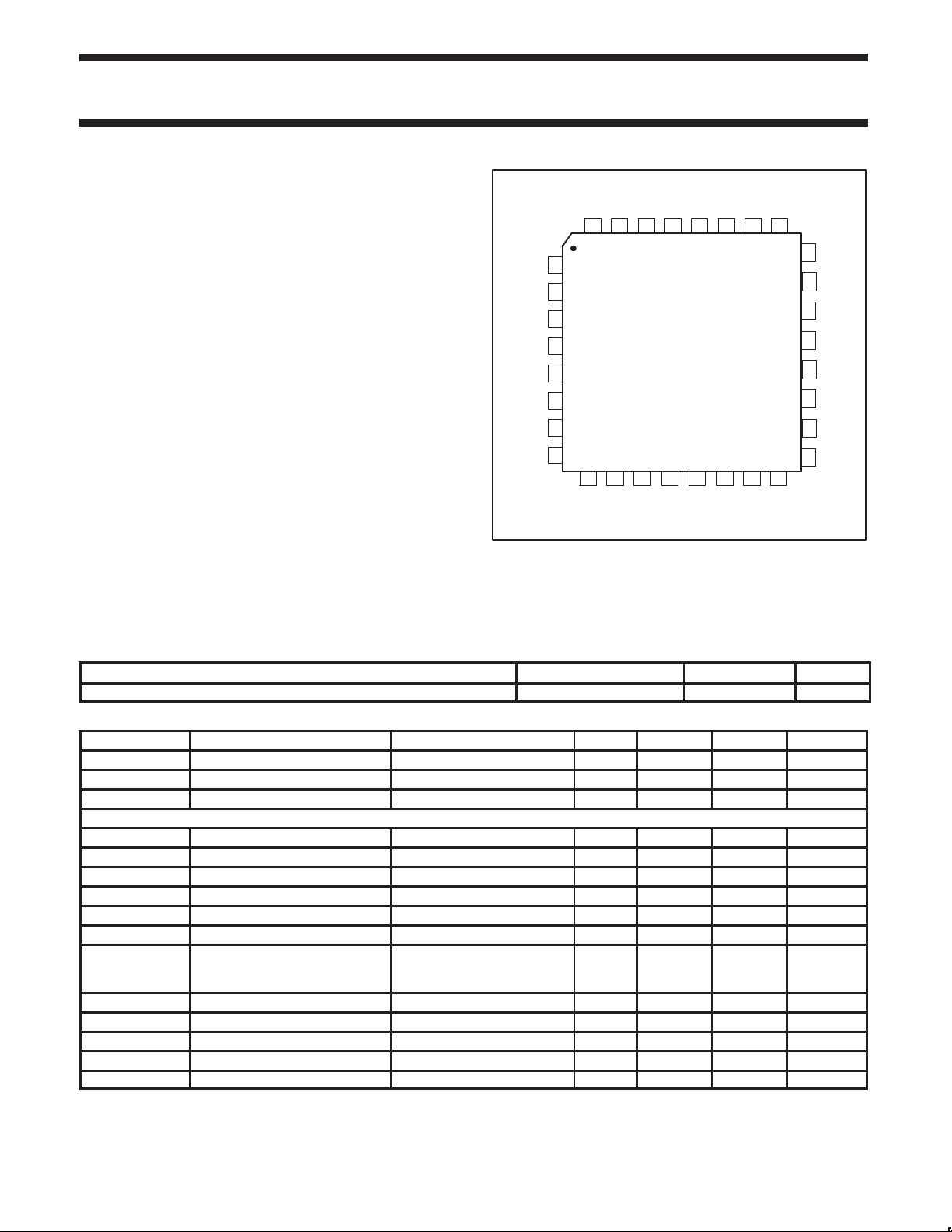
SA2410
IN
PA
GND
31 30 29 28 2 26 2532
1
D4
2
3
D3
4
5
6
7
8
10 11 12 13 14 19 16
9
SW
V
CTRL1
V
IN
SW
GND
GND
GND
GND
GND
GND
OSC
V
Figure 1. Pin Configuration
GND
CTRL2
V
V
OUT2
SW
D2
24
PA
OUT
23
GND
26
GND
GND
21
20
GND
19
GND
18
VG
PA
17
V
NEG
SR01422
ORDERING INFORMATION
DESCRIPTION TEMPERATURE RANGE ORDER CODE DWG #
32–Pin Plastic Thin Quad Flat Package –40° C+85°C SA2410 SOT401–1
GENERAL SPECIFICATIONS
Symbol Parameter Condition Min Typ Max Unit
T Temperature –40 +85 C
V
CC
I
CC
Power Amplifier
f
RF
IM3 IM3 2 tones 30 dBc
IM5 IM5 2 tones 50 dBc
T
on
T
off
Gain Small signal gain 29 dB
P
out
Eff. Efficiency 25 %
∆ Gt1 Gain variation with temp –40 to +85°C "3.5 dB
∆ Gt2 Gain variation with temp 0–70°C "2.0 dB
∆ Gr Ripple 2.45"0.05 GHz "1 dB
∆ Gvd Gain variation with supply 3.3 volts"0.3 V 0.5 dB
Supply V 3 5.5 V
Supply I 3.3 volts 125 mA
Frequency Range 2.4 2.5 GHz
Transmit power on Including neg. supply 2 µs
Xmit power down 2 µs
IM3=30dBc
Output power
IM5=50dBc
17.5 18.5 dBm
125mA@3.3 volts
1997 Sep 09
2
Page 3

Philips Semiconductors Preliminary specification
2.45GHz RF power amplifier and T/R switch
Symbol
Negative voltage supply
t
on
Linear Gain Control
Symbol Parameter Condition Min Typ Max Unit
V
GC
C
GC
G
CR
Transmit/receive switch
Symbol Parameter Condition Min Typ Max Unit
L
tx
L
rx
t
sw
ISO
PA
Z
in
Z
out
ISO
SW
Parameter Condition Min Typ Max Unit
Power on time 10 100 nS
4 GHz spur Xmit Mode TBD dBm
Gain control voltage TBD Volt
Input C at gain pin TBD pF
Attenuation range 16 dB
Insertion loss T
Insertion loss R
x
x
1.3 2 dB
1.3 2 dB
Switch response time 400 nS
Isolation switch to PA 30 dB
Input impedance 50 Ω
Output impedance 50 Ω
Switch Isolation 17 19 dB
SA2410
SW
OUT1
Attenuator
PA
IN
Negative
Power Supply
Switch
SW
IN
PA
PA
OUT
V
GPA
V
NEG
SW
OUT2
SR01423
Figure 2. Block Diagram
1997 Sep 09
3
Page 4

Philips Semiconductors Preliminary specification
SA24102.45GHz RF power amplifier and T/R switch
LQFP32: plastic low profile quad flat package; 32 leads; body 5 x 5 x 1.4 mm SOT401-1
1997 Sep 09
4
Page 5

Philips Semiconductors Preliminary specification
SA24102.45GHz RF power amplifier and T/R switch
NOTES
1997 Sep 09
5
Page 6

Philips Semiconductors Preliminary specification
SA24102.45GHz RF power amplifier and T/R switch
DEFINITIONS
Data Sheet Identification Product Status Definition
Objective Specification
Preliminary Specification
Product Specification
Formative or in Design
Preproduction Product
Full Production
Philips Semiconductors and Philips Electronics North America Corporation reserve the right to make changes, without notice, in the products,
including circuits, standard cells, and/or software, described or contained herein in order to improve design and/or performance. Philips
Semiconductors assumes no responsibility or liability for the use of any of these products, conveys no license or title under any patent, copyright,
or mask work right to these products, and makes no representations or warranties that these products are free from patent, copyright, or mask
work right infringement, unless otherwise specified. Applications that are described herein for any of these products are for illustrative purposes
only. Philips Semiconductors makes no representation or warranty that such applications will be suitable for the specified use without further testing
or modification.
LIFE SUPPORT APPLICA TIONS
Philips Semiconductors and Philips Electronics North America Corporation Products are not designed for use in life support appliances, devices,
or systems where malfunction of a Philips Semiconductors and Philips Electronics North America Corporation Product can reasonably be expected
to result in a personal injury. Philips Semiconductors and Philips Electronics North America Corporation customers using or selling Philips
Semiconductors and Philips Electronics North America Corporation Products for use in such applications do so at their own risk and agree to fully
indemnify Philips Semiconductors and Philips Electronics North America Corporation for any damages resulting from such improper use or sale.
Philips Semiconductors
811 East Arques Avenue
P.O. Box 3409
Sunnyvale, California 94088–3409
Telephone 800-234-7381
This data sheet contains the design target or goal specifications for product development. Specifications
may change in any manner without notice.
This data sheet contains preliminary data, and supplementary data will be published at a later date. Philips
Semiconductors reserves the right to make changes at any time without notice in order to improve design
and supply the best possible product.
This data sheet contains Final Specifications. Philips Semiconductors reserves the right to make changes
at any time without notice, in order to improve design and supply the best possible product.
Philips Semiconductors and Philips Electronics North America Corporation
register eligible circuits under the Semiconductor Chip Protection Act.
Copyright Philips Electronics North America Corporation 1996
All rights reserved. Printed in U.S.A.
Date of release: 09–97
Document order number: 9397 750 03299
1997 Sep 09
6
 Loading...