

Page 1
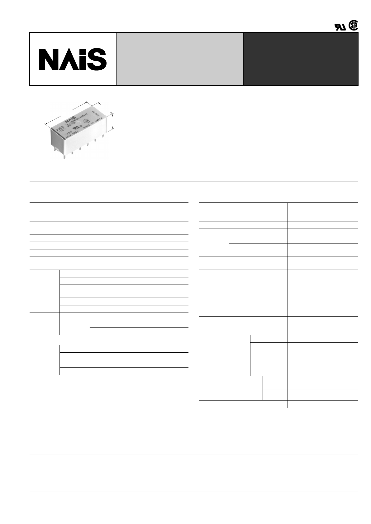
4 AMP POLARIZED HIGH
DENSITY RELAY WITH HIGH
S-RELAYS
SENSITIVITY
FEATURES
28.0
1.102
12.0
.472
10.4
.409
mm inch
• A variety of contact arrangements 2
Form A 2 Form B, 3 Form A 1 Form B,
4 Form A
• Latching types available
• High sensitivity in small size 100 mW
pick-up and 200 mW nominal operating
power
• High shock and vibration resistance
Shock: 50 G Vibration: 10 to 55 Hz at
double amplitude of 3 mm .118 inch
• Wide switching range From 100 µ A
100 mV DC to 4 A 250 V AC
• Low thermal electromotive force Approx. 3 µ V
• Dual-In-Line packaging arrangement
• Amber types available
SPECIFICATIONS
Contacts
Arrangement
Initial contact resistance, max.
(By voltage drop 6 V DC 1 A)
Initial contact pressure Approx. 12 g .42 oz
Contact material Gold clad silver alloy
Electrostatic capacitance Approx. 3pF
Thermal electromotive force
(at nominal coil voltage)
Nominal switching capacity 4 A 250 V AC, 3 A 30 V DC
Maximum switching power 1,000 VA, 90 W
Rating
(resistive)
Maximum switching voltage
Max. switching current 4 A (AC), 3 A (DC)
1
Expected
life (min.
operations)
Min. switching capacity**
Mechanical (at 50 cps) 10
Electrical
(at 20 cpm)
4 A 250 V AC 10
3 A 30 V DC 2 × 10
Coil (polarized) (at 20 ° C 68 ° F)
Single side
stable
Latching
Notes:
1
**
This value can change due to the switching frequency , en vironmental conditions,
and desired reliability level, therefore it is recommended to chec k this with the actual load.
Remarks
* Specifications will vary with foreign standards certification ratings.
1
Measurement at same location as "Initial breakdown voltage "section
*
2
*
Detection current: 10mA
3
Excluding contact bounce time
*
4
*
Half-wave pulse of sine wave: 11ms; detection time: 10 µ s
5
*
Half-wave pulse of sine wave: 6ms
6
Detection time: 10 µ s
*
7
*
Refer to 5. Conditions for operation, transport and storage mentioned in
AMBIENT ENVIRONMENT (Page 61).
Minimum operating power Approx. 100 mW
Nominal operating power Approx. 200 mW
Minimum set and reset Approx. 100 mW
Nominal set and reset Approx. 200 mW
2 Form A 2 Form B,
3 Form A 1 Form B,
4 Form A
50 m Ω
Approx. 3 µ V
250 V AC, 30 V DC
(48 VDC at less than 0.5 A)
100 µ A 100 m V DC
8
5
5
Characteristics (at 25 ° C 77 ° F 50% Relative humidity)
Max. operating speed
Initial insulation resistance*
Initial
breakdown
voltage*
Operate time*
Between open contacts 750 Vrms
Between contact sets 1,000 Vrms
2
Between contacts and
coil
3
1
(at nominal voltage)(at 20 ° C)
Release time (without diode)*
3
(at nominal voltage)(at 20 ° C)
Set time*
3
(latching)
(at nominal voltage)(at 20 ° C)
Reset time*
3
(latching)
(at nominal voltage)(at 20 ° C)
Initial contact bounce, max. 1 ms
Temperature rise
(at nominal voltage)(at 20 ° C)
Shock resistance
Functional*
Destructive*
Functional*
Vibration resistance
Destructive
Conditions for operation,
transport and storage*
(Not freezing and condensing at low temperature)
Ambient
7
temp.
Humidity 5 to 85% R.H.
Unit weight Approx. 8 g .28 oz
20 cpm for maximum load,
50 cps for low-level load
(1 mA 1 V DC)
10,000 M Ω at 500 V DC
1,500 Vrms
Max. 15 ms (Approx. 8 ms)
Max. 10 ms (Approx. 5 ms)
Max. 15 ms (Approx. 8 ms)
Max. 15 ms (Approx. 8 ms)
Max. 35 ° C with nominal coil
voltage and at maximum
switching current
4
5
6
Min. 490 m/s
Min. 980 m/s
176.4 m/s
2
{18 G}, 10 to 55 Hz
at double amplitude of 3 mm
235.2 m/s
2
{24 G}, 10 to 55 Hz
at double amplitude of 4 mm
–40 ° C to +65 ° C
–40 ° F to +149 ° F
2
{50 G}
2
{100 G}
TYPICAL APPLICATIONS
Telecommunications equipment, data processing equipment,
facsimiles, alarm equipment, measuring equipment.
219
Page 2
S
ORDERING INFORMATION
Ex.
Ω ( ±
Ω ( ±
S 2 EB L2 48V
Contact arrangement Classification of type
2: 2 Form A 2 Form B
EB: Amber sealed type
3: 3 Form A 1 Form B
Operating function
Nil: Single side stable
L2: 2 coil latching
Coil voltage (DC)
3, 5, 6, 12, 24, 48 V
4: 4 Form A
(Notes) 1. Standard packing Carton: 50 pcs. Case: 500 pcs.
2. 1 coil latching also available as option. Contact our sales office for details.
3. UL/CSA approved type is standard.
TYPES AND COIL DATA at 20 ° C 68 ° F
Single side stable
Nominal
operating
current,
mA
Coil resistance,
10%)
Inductance,
mH
Type
Nominal
voltage,
V DC
Pick-up
voltage,
V DC (max.)
Drop-out
voltage,
V DC (min.)
S ❑ EB-3V 3 2.1 0.3 66.7 45 23 200 5.5
S ❑ EB-5V 5 3.5 0.5 38.5 130 65 192 9.0
S ❑ EB-6V 6 4.2 0.6 33.3 180 93 200 11.0
S ❑ EB-12V 12 8.4 1.2 16.7 720 370 200 22.0
S ❑ EB-24V 24 16.8 2.4 8.4 2,850 1,427 202 44.0
S ❑ EB-48V 48 33.6 4.8 5.6 8,500 3,410 271 75.0
Nominal
operating
power,
mW
Maximum
allowable
voltage,
V DC (40 ° C)
2 coil latching
Nominal
operating
power,
mW
Type
Nominal voltage,
V DC
Set and reset
voltage,
V DC (max.)
Nominal operating
current,
mA
Coil resistance,
10%)
Inductance,
mH
S ❑ EB-L2-3V 3 2.1 66.7 45 45 10 10 200 5.5
S ❑ EB-L2-5V 5 3.5 38.5 130 130 31 31 192 9.0
S ❑ EB-L2-6V 6 4.2 33.7 180 180 40 40 200 11.0
S ❑ EB-L2-12V 12 8.4 16.7 720 720 170 170 200 22.0
S ❑ EB-L2-24V 24 16.8 8.4 2,850 2,850 680 680 202 44.0
S ❑ EB-L2-48V 48 33.6 7.4 6,500 6,500 1,250 1,250 355 65.0
Note: Insert 2, 3 or 4 in ❑ for contact form reguired.
Maximum
allowable
voltage,
V DC (40 ° C)Coil I Coil II Coil I Coil II
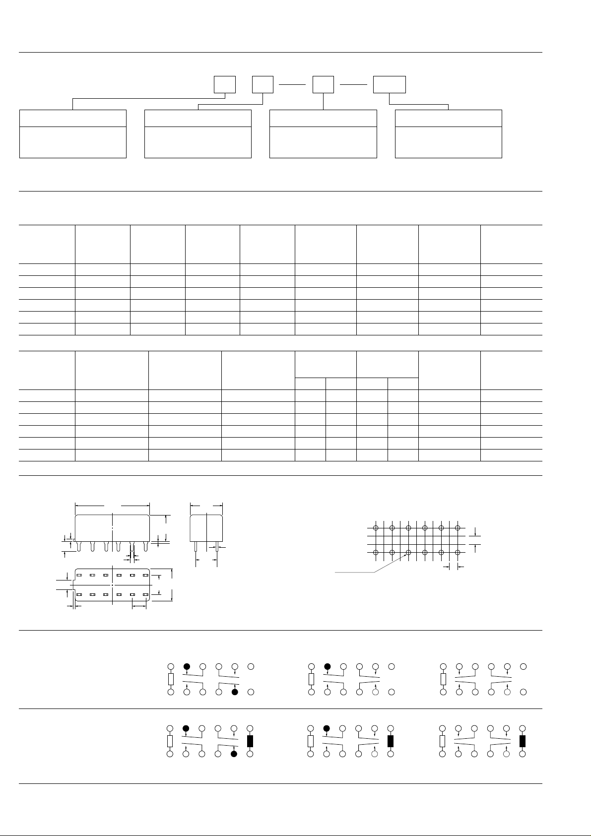
DIMENSIONS
1.102±0.02
1
.039
4
.157
3
123456
.118
12 11 10 9 8 7
0.5
.020
28±0.5
1.4
.055
12
.472
10±0.5
.394±0.02
0.4
1.0
.039
5.08
.200
.016
7.62
.300
12
.472
7.62
.300
General tolerance: ± 0.3 ± .012
0.5
.020
PC board pattern (Copper-side view)
12-1.3 DIA.
.047-.051 DIA.
2.54
.100
2.54
.100
Tolerance: ± 0.1 ± .003
mm inch
Schematic
(Bottom view)
Single side stable
Deenergized position
2 coil latching
Diagram shows the "reset"
position when terminals 6
and 7 are energized.
Energize terminals 1 and
12 to transfer contacts.
220
2a2b 3a1b 4a
2a2b 3a1b 4a
123456
+
-
12 11 10 9 8 7
123456
+
Set Reset
-
12 11 10 9 8 7
+
-
123456
+
-
12 11 10 9 8 7
123456
+
Set Reset
-
12 11 10 9 8 7
+
-
123456
+
-
12 11 10 9 8 7
123456
+
Set Reset
-
12 11 10 9 8 7
+
-
Page 3

REFERENCE DATA
1. Maximum switching power 2. Life curve 3. Contact reliability
1,000
100
Contact voltage, V
DC resistive load
10
AC resistive load
0.1 1 10
Contact current, A
1,000
500
4
100
Life, ×10
50
30
10
012345
Contact current, A
125 V AC
(cosϕ = 1.0)
250 V AC
(cosϕ = 1.0)
Condition: 1V DC, 1mA
Detection level 10 Ω
Tasted Sample: S4EB-24V, 10pcs
99.9
99.0
95.0
70.0
50.0
30.0
10.0
5.0
2.0
1.0
0.5
0.2
0.1
m = 1.6
µ: 79 million time
σ: 51 million time
95% reliability limit:
14.6 million times
(weibul probability paper)
1.0 10.0
No. of operations, ×10
S
7
4.-(1) Coil temperature rise
Tested Sample: S4EB-24V, 4 Form A
100
90
80
70
60
50
40
Temperature rise, °C
30
20
10
0
0.2 0.4 0.6 0.8 1.0 1.2
Coil operating power, W
4A
0A
5.-(2) Operate time (2 coil latching type)
Tested Sample: S2EB-L2-12V
20
18
16
14
12
10
8
Operate/release time, ms
Max.
6
Min.
4
2
(without diode)
80 100 120 140
(with diode)
Coil applied voltage, %V
Max.
Min.
4.-(2) Coil temperature rise
Tested Sample: S4EB-24V, 4 Form A
100
90
80
70
60
50
40
Temperature rise, °C
Coil operating
30
power, 0.2 W
20
10
0
123456
Contact current, A
6. Influence of adjacent mounting
(1) (2) (3)
Single side stable 2 coil latching
+30
0
Rate of change, %
–30
(1) & (3) relays
are energized
Drop-out voltage
Pick-up voltage
510
Inter-relay distance, mm Inter-relay distance, mm
5.-(1) Operate and release time
(Single side stable type)
Tested Sample: S4EB-24V, 10pcs
20
18
16
14
12
10
8
Operate/release time, ms
6
4
Max.
Min.
2
0
Note: When installing an S-relay near another, and there is no effect
from an external magnetic field, be sure to leave at least 10 mm
.394 inch between relays in order to acheive the performance
listed in the catalog.
+30
0
Rate of change, %
–30
Release time (with diode)
Operate time
Release time
80 100 120 140
Coil applied voltage, %V
Pick-up voltage
510
Max.
Min.
Max.
Min.
7. Thermal electromotive force
200
NR-H
100
Thermal electromotive force, µV
2 4 6 8 10 12
Minute
NF relay
S relay
8. Effect from an external magnetic field
Single side stable
+30
0
Rate of change, %Rate of change, %
–30
2 coil latching
+30
0
–30
φ
Pick-up voltage
Drop-out voltage
50 100
G
Pick-up voltage
50 100
G
Single side stable
+30
0
Rate of change, %Rate of change, %
–30
2 coil latching
+30
0
–30
φ
Drop-out voltage
Pick-up voltage
50 100
G
Pick-up voltage
50 100
G
221
Page 4

S
ACCESSORIES
S Relay Socket,
S-PS
Specifications
Breakdown voltage 1,500 Vrms between terminals
Insulation resistance More than 100 M Ω between terminals at 500 V DC Mega
Heat resistance 150 ± 3 ° C (302 ± 5.4°F) for 1 hour.
Maximum continuous current 4 A
(Note: Don't insert or remove relays while in the energized condition.)
Dimensions
12.4±0.6
.488±.024
18.3±0.6
.720±.024
1.2±0.3
.047±.012
4.85±0.3
.191±.012
.059±.012
1.5±0.3
5.08±0.3
.200±.012
32.4±0.6
1.276±.024
15.5±0.6
.610±.024
1.5±0.3
.059±.012
Inserting and removing method
Inserting method: Insert the relay as
shown in Fig. 1 unit the rib of the relay
snaps into the clip of the socket.
Removing method:
(1) Remove the relay straight from the
socket holding the shaded portion of the
relay as shown in Fig. 2.
0.4±0.1
.016±.004
3.4±0.3
7.62±0.3
.300±.012
Terminal width: 1.3 .051
Terminal thickness: 1.2 .047
.134±.012
mm inch
PC board pattern (Copper-side view)
7.6
.299
5.08
5.08
5.08
5.08
.200
.200
5.08
.200
.200
12-1.6 DIA. HOLE
12-.063 DIA. HOLE
Rib
Fig. 1
Fig. 2
.200
(2) When sockets are mounted in close
proximity, use a slotted screw driver as
shown in Fig. 3.
NOTES
1. Special use of 2 coil latching types: 2
ways can be considered if 2 coil latching
types are used as 1 coil latching types.
(A) Reverse polarity is applied to the set
coil of 2 coil latching type.
(B) By shorting terminals 12 and 7, apply
plus to 1, minus to 6 at set and plus to 6,
minus to 1 at reset. Applied coil voltage
should be the same as the nominal. Operating power will be reduced to one-half.
Reset position of 2a2b type 2. Soldering operations should be accom-
123456
-
12 11 10 9 8 7
CAUTIONS FOR USE
Based on regulations regarding insulation distance, there is a restriction on same-channel load connections between terminals
No. 2, 3 and 4, 5, as well as between No . 8, 9 and 10, 11. See the
figure below for an example.
Fig. 3
+
23
11
• Between 2, 3 and 4, 5:
• Between 10, 11 and 8, 9:
plished as quick as possible; within 10
seconds at 250°C 482°F solder temperature or 3 seconds at 350°C 662°F. The
header portion being sealed with epoxy
resin, undue subjection to heat may
cause loss of seal. Solder should not be
permitted to remain on the header.
5
4
3
9
10
different channels, therefore not possible
different channels, therefore not possible
8
• Between 2, 3 and 4, 5:
• Between 10, 11 and 8, 9:
No good Good
2
11
10
same channels, therefore possible
same channels, therefore possible
4
5
8
9
For Cautions for Use, see Relay Technical Information (Page 48 to 76).
222
9/1/2000 All Rights Reserved, © Copyright Matsushita Electric Works, Ltd.
Go To Online Catalog
 Loading...