

Page 1
July 1998
Semiconductor
RFM7N35, RFM7N40,
RFP7N35, RFP7N40
7A, 350V and 400V, 0.75 Ohm,
N-Channel Power MOSFETs
Features
• 7A, 350V and 400V
•r
• SOA is Power Dissipation Limited
• Nanosecond Switching Speeds
• Linear Transfer Characteristics
• High Input Impedance
• Majority Carrier Device
• Related Literature
- TB334 “Guidelines for Soldering Surface Mount
= 0.75Ω
DS(ON)
Components to PC Boards”
Ordering Information
PART NUMBER PACKAGE BRAND
RFM7N35 TO-204AA RFM7N35
RFM7N40 TO-204AA RFM7N40
RFP7N35 TO-220AB RFP7N35
RFP7N40 TO-220AB RFP7N40
Description
These are N-Channel enhancement mode silicon gate
power field effect transistors designed for applications such
as switching regulators, switching converters, motor drivers,
relay drivers and drivers for high power bipolar switching
transistors requiring high speed and low gate drive power.
These types can be operated directly from integrated
circuits.
Formerly developmental type TA17424.
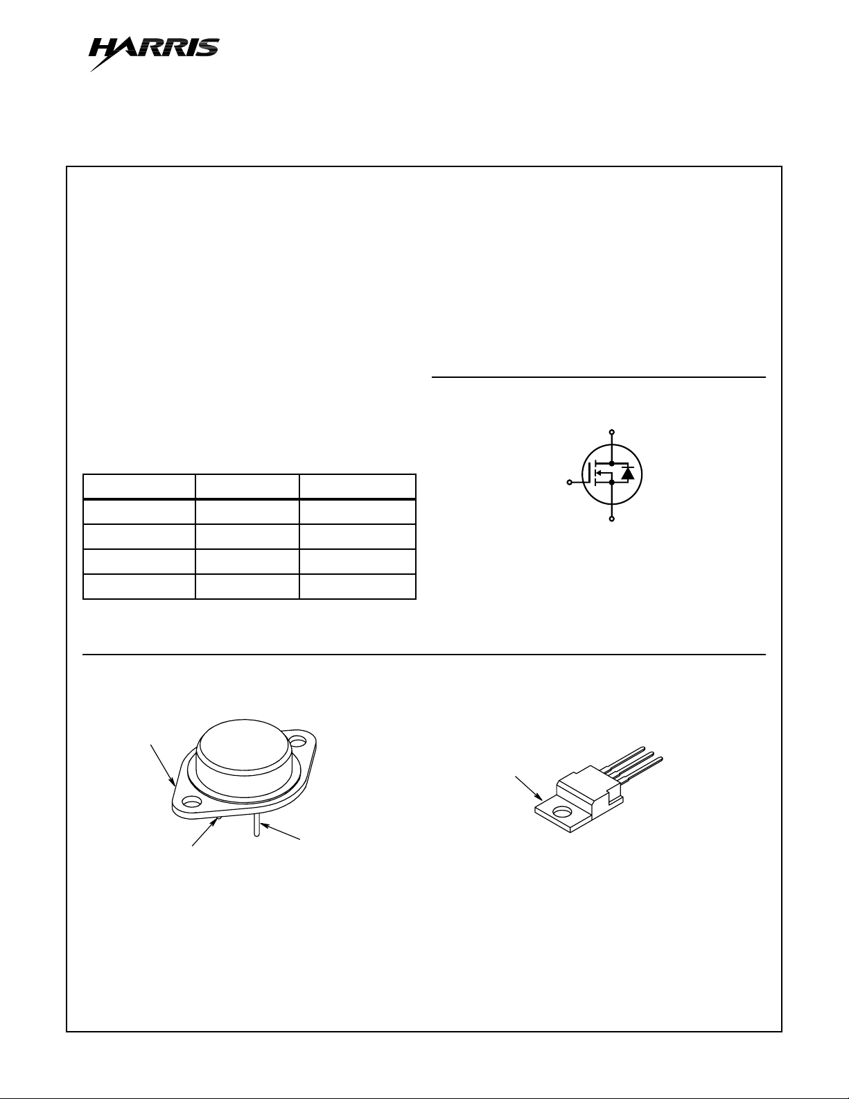
Symbol
D
G
S
NOTE: When ordering, use the entire part number.
Packaging
JEDEC TO-204AA JEDEC TO-220AB
DRAIN
(FLANGE)
GATE (PIN 1)
SOURCE (PIN 2)
DRAIN
(TAB)
SOURCE
DRAIN
GATE
CAUTION: These devices are sensitive to electrostatic discharge. Users should follow proper ESD Handling Procedures.
Copyright
© Harris Corporation 1998
5-1
File Number 1536.2
Page 2

RFM7N35, RFM7N40, RFP7N35, RFP7N40
Absolute Maximum Ratings T
= 25oC, Unless Otherwise Specified
C
RFM7N35 RFM7N40 RFP7N35 RFP7N40 UNITS
Drain to Source Voltage (Note 1) . . . . . . . . . . . . . . . . . . . . . . . . . . . . V
Drain to Gate Voltage (RGS = 1MΩ) (Note 1). . . . . . . . . . . . . . . . . . . V
DSS
DGR
Continuous Drain Current. . . . . . . . . . . . . . . . . . . . . . . . . . . . . . . . . . . . . I
Pulsed Drain Current (Note 3) . . . . . . . . . . . . . . . . . . . . . . . . . . . . . . . .I
Gate to Source Voltage . . . . . . . . . . . . . . . . . . . . . . . . . . . . . . . . . . . . V
Maximum Power Dissipation . . . . . . . . . . . . . . . . . . . . . . . . . . . . . . . . . .P
DM
GS
350 400 350 400 V
350 400 350 400 V
D
7777A
15 15 15 15 A
±20 ±20 ±20 ±20 V
100 100 75 75 W
D
Linear Derating Factor (Above 25oC) . . . . . . . . . . . . . . . . . . . . . . . . . . . . 0.8 0.8 0.6 0.6 W/oC
Operating and Storage Temperature . . . . . . . . . . . . . . . . . . . . . . TJ, T
-55 to 150 -55 to 150 -55 to 150 -55 to 150
STG
Maximum Temperature for Soldering
Leads at 0.063in (1.6mm) from Case for 10s . . . . . . . . . . . . . . . . . . . . T
Package Body for 10s, See Techbrief 334 (for TO-220) . . . . . . . . . . T
CAUTION: Stresses above those listed in “Absolute Maximum Ratings” may cause permanent damage to the device. This is a stress only rating and operation
of the device at these or any other conditions above those indicated in the operational sections of this specification is not implied.
pkg
300
L
260
300
260
300
260
300
260
o
C
o
C
o
C
NOTE:
1. TJ= 25oC to 125oC.
Electrical Specifications T
= 25oC, Unless Otherwise Specified
C
PARAMETER SYMBOL TEST CONDITIONS MIN TYP MAX UNITS
Drain to Source Breakdown Voltage BV
DSS
ID = 250µA, VGS = 0V
RFM7N35, RFP7N35 350 - - V
RFM7N40, RFP7N40 400 - - V
Gate Threshold Voltage V
GS(TH)
Zero Gate Voltage Drain Current I
Gate to Source Leakage Current I
Drain to Source On Resistance (Note 2) r
Drain to Source On Voltage (Note 2) V
Turn-On Delay Time t
DS(ON)ID
DS(ON)ID
d(ON)
Rise Time t
Turn-Off Delay Time t
d(OFF)
Fall Time t
Input Capacitance C
Output Capacitance C
Reverse-Transfer Capacitance C
Thermal Resistance Junction to Case R
DSS
GSS
r
f
ISS
OSS
RSS
θJC
VGS = VDS, ID = 250µA (Figure 8) 2 - 4 V
VDS = Rated BV
V
= 0.8 x Rated BV
DS
, TC = 25oC--1µA
DSS
, TC = 125oC- - 25 µA
DSS
VGS = ±20V, VDS = 0V - - ±100 nA
= 7A, VGS = 10V (Figures 6, 7) - - 0.75 Ω
= 7A, VGS = 10V - - 5.25 V
VDS = 200V, I
RL = 56Ω, VGS = 10V
(Figures 10, 11, 12)
≈ 3.5A, R
D
= 50Ω,
G
-1645ns
-5475ns
- 170 250 ns
- 62 100 ns
VDS = 25V, VGS = 0V, f = 1MHz
(Figure 9)
- - 1600 pF
- - 300 pF
- - 200 pF
RFM7N35, RFM7N40 - - 1.25oC/W
RFP7N35, RFP7N40 - - 1.67oC/W
Source to Drain Diode Specifications
PARAMETER SYMBOL TEST CONDITIONS MIN TYP MAX UNITS
Source to Drain Diode Voltage (Note 2) V
Reverse Recovery Time t
SD
rr
NOTES:
2. Pulse Test: Pulse Width ≤ 300µs, duty cycle ≤ 2%.
3. Repetitive rating: pulse width limited by maximum junction temperature.
ISD = 7A - - 1.4 V
ISD = 7A, dISD/dt = 100A/µs - 870 - ns
5-2
Page 3

RFM7N35, RFM7N40, RFP7N35, RFP7N40
Typical Performance Curves
1.2
1.0
0.8
0.6
0.4
0.2
POWER DISSIPATION MULTIPLIER
0
0 50 100 150
TC, CASE TEMPERATURE (oC)
Unless Otherwise Specified
FIGURE 1. NORMALIZED POWER DISSIP ATION vs CASE
TEMPERA TURE
100
TC = 25oC
T
= MAX RATED
J
ID (MAX)
CONTINUOUS
10
OPERATION IN
1
, DRAIN CURRENT (A)
D
I
0
1 10 100 1000
THIS AREA IS
LIMITED BY r
V
, DRAIN TO SOURCE VOLTAGE (V)
DS
DC OPERA
TION
DS(ON)
RFM7N35, RFP7N35
RFM7N40, RFP7N40
RFM7N35, 40
RFP7N35, 40
8
7
6
5
4
3
, DRAIN CURRENT (A)
2
D
I
1
0
25 50 75 100 125 150
RFP7N40
, CASE TEMPERATURE (oC)
T
C
RFM7N40
FIGURE 2. MAXIMUM CONTINUOUS DRAIN CURRENT vs
CASE TEMPERATURE
16
PULSE DURATION = 80µs
T
= 25oC
C
12
VGS = 7V TO 20V
8
, DRAIN CURRENT (A)
4
D
I
0
04 8121620
VDS, DRAIN TO SOURCE VOLTAGE (V)
VGS = 6V
VGS = 5V
VGS = 4V
FIGURE 3. FORWARD BIAS SAFE OPERATING AREA FIGURE 4. SATURATION CHARACTERISTICS
16
VDS = 10V
PULSE DURATION = 250µs
12
TC = 25oC
8
TC = 125oC
4
, DRAIN TO SOURCE CURRENT (A)
DS(ON)
0
I
0246810
V
, GATE TO SOURCE (V)
GS
TC = -40oC
1.8
TC = 125oC
1.4
1
TC = 25oC
, DRAIN TO SOURCE
ON RESISTANCE (Ω)
0.6
DS(ON)
r
0.2
048121620
I
, DRAIN CURRENT (A)
D
VGS = 10V
PULSE DURATION = 250µs
TC = -40oC
FIGURE 5. TRANSFER CHARA CTERISTICS FIGURE 6. DRAIN TO SOURCE ON RESIST ANCE vs GATE
VOLTAGE AND DRAIN CURRENT
5-3
Page 4

RFM7N35, RFM7N40, RFP7N35, RFP7N40
Typical Performance Curves
= 10V
V
GS
ID = 7A
2
1.5
1
ON RESISTANCE
0.5
NORMALIZED DRAIN TO SOURCE
-50 0 50 100 150 200
, JUNCTION TEMPERATURE (oC)
T
J
Unless Otherwise Specified (Continued)
FIGURE 7. NORMALIZED DRAIN TO SOURCE ON
RESISTANCE vs JUNCTION TEMPERATURE
1600
1400
1200
C
C
RSS
ISS
C
OSS
, DRAIN TO SOURCE (V)
V
DS
1000
800
600
400
C, CAPACITANCE (pF)
200
0
0 1020304050
VGS = 0V, f = 1MHz
C
= CGS + C
ISS
C
= C
RSS
OSS
GD
≈ CDS + C
C
FIGURE 9. CAPACITANCE vs DRAIN TO SOURCE VOLTAGE
GD
GS
1.4
ID = 250µA
1.2
1
NORMALIZED GATE
0.8
THRESHOLD VOLTAGE
0.6
-50 0 50 100 150 200
, JUNCTION TEMPERATURE (oC)
T
J
FIGURE 8. NORMALIZED GATE THRESHOLD V OLTA GE vs
JUNCTION TEMPERATURE
, (V)
DS
V
400
300
200
100
BV
DSS
VDD = V
DSS
DRAIN TO SOURCE VOLTAGE
0
I
G(REF)
20
I
G(ACT)
GATE
TO
SOURCE
VOLTAGE
0.75 V
DSS
0.50 V
DSS
0.25 V
DSS
t, TIME (µs)
I
G(REF)
RL = 57Ω
= 0.45mA
= 10V
V
GS
VDD = V
80
DSS
I
G(REF)
I
G(ACT)
NOTE: Refer to Harris Application Notes AN7254 and AN7260.
FIGURE 10. NORMALIZED SWITCHING WAVEFORMS FOR
CONSTANT GATE CURRENT
10
8
6
, (V)
4
GS
V
2
0
Test Circuits and Waveforms
R
G
V
GS
FIGURE 11. SWITCHING TIME TEST CIRCUIT FIGURE 12. RESISTIVE SWITCHING WAVEFORMS
t
ON
t
d(ON)
t
R
L
+
V
DD
-
DUT
V
DS
0
V
GS
10%
0
r
90%
10%
50%
PULSE WIDTH
t
d(OFF)
90%
t
OFF
50%
t
f
90%
10%
5-4
 Loading...