

Page 1
Semiconductor
/
September 1998
RFP45N03L,
RF1S45N03L, RF1S45N03LSM
45A, 30V, 0.022 Ohm,
Logic Level, N-Channel Power MOSFETs
[ /Title
(RFP45
N03L,
RF1S45
N03L,
RF1S45
N03LS
M)
Subject
(45A,
30V,
0.022
Ohm,
Features
• 45A, 30V
•r
DS(ON)
Temperature Compensating
•
• Can be Driven Directly from CMOS, NMOS, and TTL
Circuits
• Peak Current vs Pulse Width Curve
• UIS Rating Curve
• 175
• Related Literature
- TB334 “Guidelines for Soldering Surface Mount
= 0.022Ω
PSPICE Model
o
C Operating Temperature
Components to PC Boards”
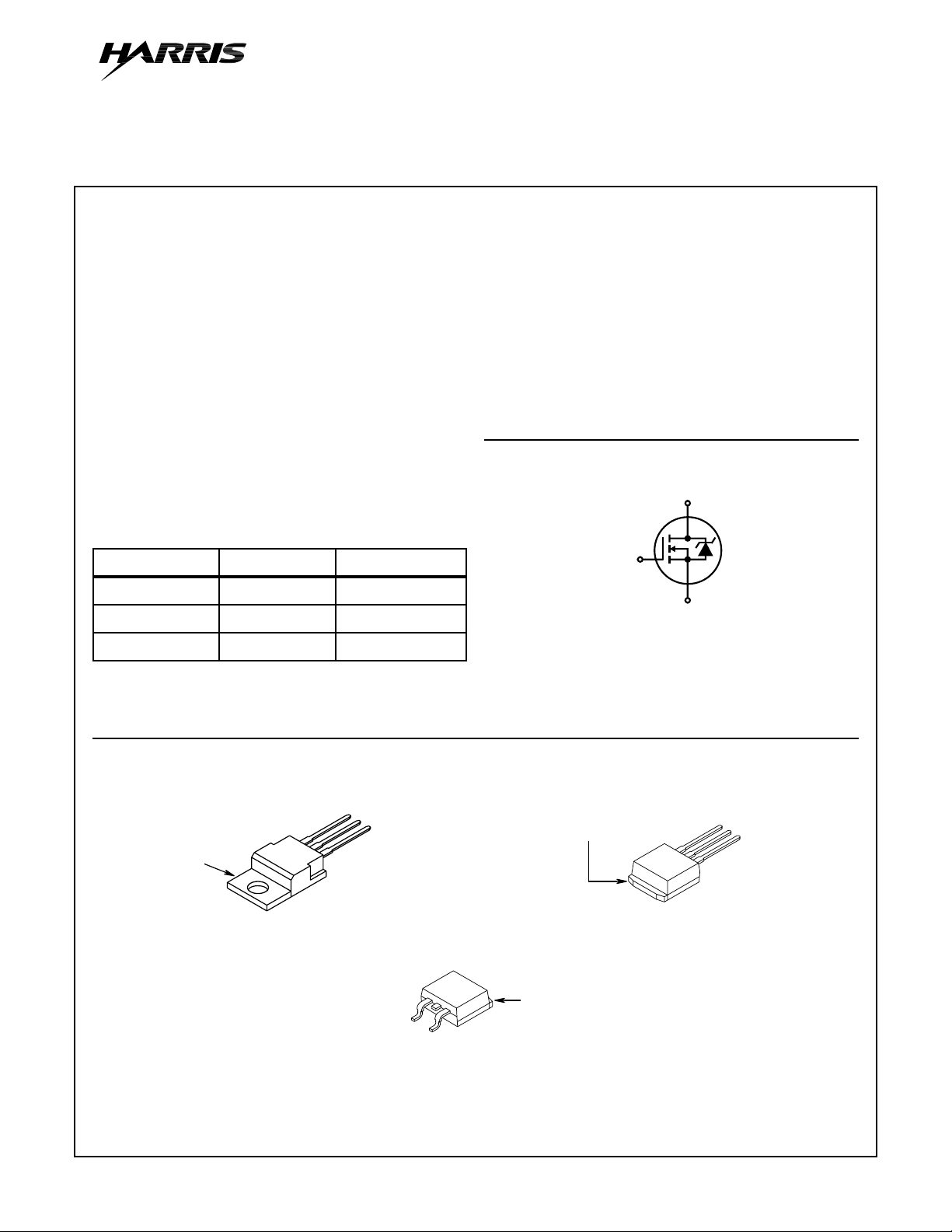
Ordering Information
PART NUMBER PACKAGE BRAND
RFP45N03L TO-220AB FP45N03L
RF1S45N03L TO-262AA F45N03L
RF1S45N03LSM TO-263AB F45N03L
Description
These are N-Channel power MOSFETs manufactured using
the MegaFET process. This process, which uses feature
sizes approaching those of LSI circuits, gives optimum utilization of silicon, resulting in outstanding performance. They
were designed for use in applications such as switching regulators, switching conv erters, motor drivers and rela y drivers .
These transistors can be operated directly from integrated
circuits.
Formerly developmental type TA49030.
Symbol
D
G
S
NOTE: When ordering, use the entire part number. Add the suffix 9A, to
obtain the TO-263AB variant in tape and reel, e.g., RF1S45N03LSM9A.
Packaging
JEDEC TO-220AB JEDEC TO-262AA
SOURCE
DRAIN
GATE
DRAIN (FLANGE)
JEDEC TO-263AB
GATE
SOURCE
(FLANGE)
DRAIN
(FLANGE)
DRAIN
SOURCE
DRAIN
GATE
CAUTION: These devices are sensitive to electrostatic discharge. Users should follow proper ESD Handling Procedures.
Copyright
© Harris Corporation 1998
7-1
File Number 4005.2
Page 2
RFP45N03L, RF1S45N03L, RF1S45N03LSM
Absolute Maximum Ratings T
= 25oC, Unless Otherwise Specified
C
RFP45N03L, RF1S45N03L,
RF1S45N03LSM UNITS
Drain to Source Voltage (Note 1) . . . . . . . . . . . . . . . . . . . . . . . . . . . . . . . . . . . . V
Drain to Gate Voltage RGS = 20kΩ (Note 1) . . . . . . . . . . . . . . . . . . . . . . . . . . . V
Gate to Source Voltage . . . . . . . . . . . . . . . . . . . . . . . . . . . . . . . . . . . . . . . . . . . . V
Continuous Drain Current. . . . . . . . . . . . . . . . . . . . . . . . . . . . . . . . . . . . . . . . . . . . . I
Pulsed Drain Current (Note 3) . . . . . . . . . . . . . . . . . . . . . . . . . . . . . . . . . . . . . . I
Pulsed Avalanche Rating . . . . . . . . . . . . . . . . . . . . . . . . . . . . . . . . . . . . . . . . . . . .E
Power Dissipation. . . . . . . . . . . . . . . . . . . . . . . . . . . . . . . . . . . . . . . . . . . . . . . . . . .P
DSS
DGR
GS
DM
AS
D
Refer to Peak Current Curve
D
Derate Above 25oC. . . . . . . . . . . . . . . . . . . . . . . . . . . . . . . . . . . . . . . . . . . . . . . . . .
Operating and Storage Temperature . . . . . . . . . . . . . . . . . . . . . . . . . . . . . . .TJ,T
STG
Maximum Temperature for Soldering
Leads at 0.063in (1.6mm) from Case for 10s . . . . . . . . . . . . . . . . . . . . . . . . . . . . T
Package Body for 10s, See Techbrief 334 . . . . . . . . . . . . . . . . . . . . . . . . . . . . T
CAUTION: Stresses above those listed in “Absolute Maximum Ratings” may cause permanent damage to the device. This is a stress only rating and operation
of the device at these or any other conditions above those indicated in the operational sections of this specification is not implied.
L
pkg
30 V
30 V
±10 V
45
Refer to UIS Curve
90
0.606
-55 to 175
300
260
A
W
W/oC
o
C
o
C
o
C
NOTE:
1. TJ= 25oC to 150oC.
Electrical Specifications T
= 25oC, Unless Otherwise Specified
C
PARAMETER SYMBOL TEST CONDITIONS MIN TYP MAX UNITS
Drain to Source Breakdown Voltage BV
Gate to Threshold Voltage V
GS(TH)VGS
Zero Gate Voltage Drain Current I
Gate to Source Leakage Current I
Drain to Source On Resistance (Note 2) r
DS(ON)ID
Turn-On Time t
Turn-On Delay Time t
d(ON)
Rise Time t
Turn-Off Delay Time t
d(OFF)
Fall Time t
Turn-Off Time t
Total Gate Charge Q
g(TOT)VGS
Gate Charge at 5V Q
Threshold Gate Charge Q
Input Capacitance C
Output Capacitance C
Reverse Transfer Capacitance C
Thermal Resistance Junction-to-Case R
Thermal Resistance Junction-to-Ambient R
DSSID
DSS
GSS
ON
r
f
OFF
g(5)
g(TH)
ISS
OSS
RSS
θJC
θJA
= 250µA, VGS = 0V 30 - - V
= VDS, ID = 250µA1-2V
VDS = Rated BV
VDS = Rated BV
, VGS = 0V - - 25 µA
DSS
, VGS = 0V, TC = 150oC - - 250 µA
DSS
VGS = ±10V - - ±100 nA
= 45A, VGS = 5V (Figure 11 - - 0.022 Ω
VDD = 15V, ID = 45A, RL = 0.33Ω,
VGS = 5V, RGS = 5Ω
(Figures 15, 18, 19)
- - 260 ns
-15- ns
- 160 - ns
-20- ns
-20- ns
- - 60 ns
= 0V to 10V VDD = 24V, ID = 45A,
VGS = 0V to 5V - 30 36 nC
VGS = 0V to 1V - 1.5 1.8 nC
RL = 0.533Ω
I
= 0.6mA
G(REF)
(Figures 20, 21)
VDS = 25V, VGS = 0V, f = 1MHz
(Figure 14)
-5060nC
- 1650 - pF
- 575 - pF
- 200 - pF
- - 1.65oC/W
--80oC/W
Source to Drain Diode Specifications
PARAMETER SYMBOL TEST CONDITIONS MIN TYP MAX UNITS
Source to Drain Diode Voltage V
SD
Diode Reverse Recovery Time t
NOTES:
2. Pulse test: pulse width ≤ 300µs, duty cycle ≤ 2%.
3. Repetitive rating: pulse width limited by Max junction temperature. See Transient Thermal Impedance curve (Figure 3).
ISD = 45A - - 1.5 V
ISD = 45A, dISD/dt = 100A/µs - - 125 ns
rr
7-2
Page 3
RFP45N03L, RF1S45N03L, RF1S45N03LSM
Typical Performance Curves
1.2
1.0
0.8
0.6
0.4
0.2
POWER DISSIPATION MULTIPLIER
0
0 25 50 75 100 175
TC, CASE TEMPERATURE (oC)
Unless Otherwise Specified
150
125
FIGURE 1. NORMALIZED POWER DISSIP ATION vs CASE
TEMPERA TURE
2
1
50
40
30
20
, DRAIN CURRENT (A)
D
I
10
0
25 50 75 100
TC, CASE TEMPERATURE (oC)
125
150
FIGURE 2. MAXIMUM CONTINUOUS DRAIN CURRENT vs
CASE TEMPERATURE
175
0.5
0.2
0.1
0.1
, NORMALIZED
JC
θ
Z
500
100
, DRAIN CURRENT (A)
D
I
0.05
0.02
THERMAL IMPEDANCE
0.01
SINGLE PULSE
0.01
-5
10
TC = 25oC, TJ = MAX RATED
10
OPERATION IN THIS
AREA MAY BE
LIMITED BY r
1
1
VDS, DRAIN TO SOURCE VOLTAGE (V)
-4
10
-3
10
t, RECTANGULAR PULSE DURATION (s)
-2
10
FIGURE 3. NORMALIZED MAXIMUM TRANSIENT THERMAL IMPEDANCE
500
VGS = 10V
DS(ON)
100µs
1ms
10ms
100ms
DC
10
50
100
TRANSCONDUCTANCE
MAY LIMIT CURRENT
DM
10
10
IN THIS REGION
-5
, PEAK CURRENT CAPABILITY (A)
I
-4
10
NOTES:
DUTY FACTOR: D = t
PEAK TJ = PDM x Z
-1
10
VGS = 5V
-3
10
t, PULSE WIDTH (s)
P
DM
t
1
t
2
1/t2
x R
150
+ T
JC
θ
C
TC = 25oC
10
JC
θ
0
10
FOR TEMPERATURES
ABOVE 25
CURRENT AS FOLLOWS:
10
I = I
-2
o
C DERATE PEAK
175 - T
25
-1
10
C
1
10
0
1
10
FIGURE 4. FORWARD BIAS SAFE OPERATING AREA FIGURE 5. PEAK CURRENT CAPABILITY
7-3
Page 4

RFP45N03L, RF1S45N03L, RF1S45N03LSM
Typical Performance Curves
200
100
STARTING TJ = 150oC
10
If R = 0
, AVALANCHE CURRENT (A)
tAV = (L)(IAS)/(1.3*RATED BV
AS
I
If R ≠ 0
= (L/R)ln[(IAS*R)/(1.3*RATED BV
t
AV
1
0.001
0.01
tAV, TIME IN AVALANCHE (ms)
DSS
0.1
Unless Otherwise Specified (Continued)
STARTING TJ = 25oC
- VDD)
) +1]
DSS-VDD
1
10
NOTE: Refer to Harris Application Notes AN9321 and AN9322.
FIGURE 6. UNCLAMPED INDUCTIVE SWITCHING
100
VDD= 15V
75
-55oC
175oC
25oC
100
100
V
= 10V
GS
75
50
, DRAIN CURRENT (A)
25
D
I
0
0123 5
PULSE DURATION = 250µs, TC = 25oC
VDS, DRAIN TO SOURCE VOLTAGE (V)
VGS = 5V
V
GS
V
GS
V
GS
VGS = 3V
4
= 4.5V
= 4V
= 3.5V
FIGURE 7. SATURATION CHARACTERISTICS
100
75
ID = 15A
ID = 30A
ID = 45A
, ON-STATE RESISTANCE (mΩ)
DS(ON)
r
50
ID = 2A
25
0
2.5
3.0
VGS, GATE TO SOURCE VOLTAGE (V)
PULSE DURATION = 250µs
3.5
4.0 4.5
50
25
, DRAIN TO SOURCE CURRENT (A)
DS(ON)
I
0
0
VGS, GATE TO SOURCE VOLTAGE (V)
PULSE TEST
PULSE DURATION = 250µs
DUTY CYCLE = 0.5% MAX
3.0 4.5 6.0 7.51.5
FIGURE 8. TRANSFER CHARACTERISTICS FIGURE 9. DRAIN TO SOURCE ON RESISTANCE vs GATE
VOLTAGE AND DRAIN CURRENT
350
VDD = 15V, ID = 45A, RL = 0.333Ω
300
250
200
150
100
SWITCHING TIME (ns)
50
0
010
RGS, GATE TO SOURCE RESISTANCE (Ω)
t
r
t
f
t
d(OFF)
t
d(ON)
20
30
40
50
2.0
PULSE DURATION = 250µs, VGS = 5V, ID = 45A
1.5
1.0
0.5
NORMALIZED ON RESISTANCE
0
-80 -40 0 40 80 120 160
TJ, JUNCTION TEMPERATURE (oC)
5.0
200
FIGURE 10. SWITCHING TIME vs GATE RESISTANCE FIGURE 11. NORMALIZED DRAIN TO SOURCE ON
RESISTANCE vs JUNCTION TEMPERATURE
7-4
Page 5

RFP45N03L, RF1S45N03L, RF1S45N03LSM
Typical Performance Curves
2.0
1.5
1.0
NORMALIZED GATE
0.5
THRESHOLD VOLTAGE
0
-80 -40 0 40 80 120 160
TJ, JUNCTION TEMPERATURE (oC)
Unless Otherwise Specified (Continued)
VGS = VDS, ID = 250µA
FIGURE 12. NORMALIZED GATE THRESHOLD VOLTA GE vs
JUNCTION TEMPERATURE
2500
2000
1500
1000
C, CAPACITANCE (pF)
500
0
0 5 10 15 20 25
, DRAIN TO SOURCE VOLTAGE (V)
V
DS
C
C
C
ISS
OSS
RSS
VGS = 0V, f = 0.1MHz
C
= CGS + C
C
C
ISS
RSS
OSS
= C
GD
≈ CDS + C
GD
GD
FIGURE 14. CAPACITANCE vs DRAIN TO SOURCE VOLTAGE
2.0
ID = 250µA
1.5
1.0
0.5
BREAKDOWN VOLTAGE
NORMALIZED DRAIN TO SOURCE
0
200
-80 -40 0 40 80 120 160
, JUNCTION TEMPERATURE (oC)
T
J
FIGURE 13. NORMALIZED DRAIN TO SOURCE BREAKDOWN
VOLTAGE vs JUNCTION TEMPERATURE
30
24
18
12
6
, DRAIN TO SOURCE VOLTAGE (V)
DS
V
0
= BV
V
DD
I
G REF()
--------------------- -
20
I
GACT()
DSS
0.75 BV
0.50 BV
0.25 BV
RL = 0.67Ω
= 0.6mA
I
G(REF)
V
= 5V
GS
t, TIME (µs)
DSS
DSS
DSS
VDD = BV
I
G REF()
--------------------- -
80
I
GACT()
NOTE: Refer to Harris Application Notes AN7254 and AN7260.
FIGURE 15. NORMALIZED SWITCHING WAVEFORMS FOR
CONSTANT GATE CURRENT
DSS
200
5
4
3
2
1
, GATE TO SOURCE VOLTAGE (V)
GS
V
0
7-5
Page 6

RFP45N03L, RF1S45N03L, RF1S45N03LSM
Test Circuits and Waveforms
V
DS
BV
DSS
L
VARY t
TO OBTAIN
P
REQUIRED PEAK I
V
GS
AS
R
G
+
V
DD
-
DUT
0V
P
I
AS
0.01Ω
0
t
FIGURE 16. UNCLAMPED ENERGY TEST CIRCUIT FIGURE 17. UNCLAMPED ENERGY WAVEFORMS
t
P
I
AS
t
AV
V
DS
V
DD
t
ON
t
DS
10%
d(ON)
90%
50%
t
10%
r
PULSE WIDTH
V
DS
V
R
DUT
L
+
V
DD
-
0
V
GS
0
V
GS
R
GS
V
GS
FIGURE 18. SWITCHING TIME TEST CIRCUIT FIGURE 19. RESISTIVE SWITCHING WAVEFORMS
V
I
G(REF)
DS
R
L
V
GS
+
V
DD
-
DUT
V
DD
VGS= 1V
0
Q
g(TOT)
V
DS
Q
g(5)
V
GS
Q
g(TH)
VGS= 5V
t
d(OFF)
90%
t
OFF
50%
t
f
10%
VGS= 10V
90%
I
G(REF)
0
FIGURE 20. GATE CHARGE TEST CIRCUIT FIGURE 21. GATE CHARGE WAVEFORMS
7-6
Page 7

RFP45N03L, RF1S45N03L, RF1S45N03LSM
PSPICE Electrical Model
.SUBCKT RFP45N03L 2 1 3 ; rev 11/22/94
CA 12 8 2.55e-9
CB 15 14 2.64e-9
CIN 6 8 1.45e-9
DBODY 7 5 DBDMOD
DBREAK 5 11 DBKMOD
DPLCAP 10 5 DPLCAPMOD
EBREAK 11 7 17 18 33.3
EDS 14 8 5 8 1
EGS 13 8 6 8 1
ESG 6 10 6 8 1
EVTO 20 6 18 8 1
IT 8 17 1
LDRAIN 2 5 1e-9
LGATE 1 9 4.9e-9
LSOURCE 3 7 4.9e-9
MOS1 16 6 8 8 MOSMOD M = 0.99
MOS2 16 21 8 8 MOSMOD M = 0.01
RBREAK 17 18 RBKMOD 1
RDRAIN 50 16 RDSMOD 0.14e-3
RGATE 9 20 0.89
RIN 6 8 1e9
RSCL1 5 51 RSCLMOD 1e-6
RSCL2 5 50 1e3
RSOURCE 8 7 RDSMOD 10.31e-3
RVTO 18 19 RVTOMOD 1
GATE
1
LGATE RGATE
DPLCAP
10
-
6
ESG
8
+
VTO
EVTO
20
9
+
-
18
8
S1A
12
13814
S1B
CA
EGS
-
6
RIN
S2A
15
13
S2B
13
+
6
8
EDS
+
CIN
CB
5
RSCL1RSCL2
51
+
5
ESCL
51
50
RDRAIN
16
21
MOS1
14
+
5
8
--
8
DBREAK
EBREAK
MOS2
RSOURCE
11
17
+
17
18
-
7
RBREAK
IT
DRAIN
LDRAIN
DBODY
LSOURCE
SOURCE
18
RVTO
19
VBAT
+
2
3
S1A 6 12 13 8 S1AMOD
S1B 13 12 13 8 S1BMOD
S2A 6 15 14 13 S2AMOD
S2B 13 15 14 13 S2BMOD
VBAT 8 19 DC 1
VTO 21 6 0.583
ESCL 51 50 VALUE = {(V(5,51)/ABS(V(5,51)))*(PWR(V(5,51)*1e6/176,6))}
.MODEL DBDMOD D (IS = 3.61e-13 RS = 5.06e-3 TRS1 = 3.05e-3 TRS2 = 7.57e-6 CJO = 2.16e-9 TT = 2.18e-8)
.MODEL DBKMOD D (RS = 1.66e-1 TRS1 = -2.97e-3 TRS2 = 7.57e-6)
.MODEL DPLCAPMOD D (CJO = 0.96e-9 IS = 1e-30 N = 10)
.MODEL MOSMOD NMOS (VTO = 2.313 KP = 53.82 IS = 1e-30 N = 10 TOX = 1 L = 1u W = 1u)
.MODEL RBKMOD RES (TC1 = 8.95e-4 TC2 = -1e-7)
.MODEL RDSMOD RES (TC1 = 3.82e-3 TC2 = 1.17e-5)
.MODEL RSCLMOD RES (TC1 = 2.03e-3 TC2 = 0.45e-5)
.MODEL RVTOMOD RES (TC1 = -2.27e-3 TC2 = -5.75e-7)
.MODEL S1AMOD VSWITCH (RON = 1e-5 ROFF = 0.1 VON = -4.82 VOFF= -2.82)
.MODEL S1BMOD VSWITCH (RON = 1e-5 ROFF = 0.1 VON = -2.82 VOFF= -4.82)
.MODEL S2AMOD VSWITCH (RON = 1e-5 ROFF = 0.1 VON = -2.67 VOFF= 2.33)
.MODEL S2BMOD VSWITCH (RON = 1e-5 ROFF = 0.1 VON = 2.33 VOFF= -2.67)
.ENDS
NOTE: For further discussion of the PSPICE model, consult A New PSPICE Sub-Circuit for the Power MOSFET Featuring Global
Temperature Options; written by William J. Hepp and C. Frank Wheatley.
7-7
 Loading...