

Page 1
May 1997
RFP45N02L,
RF1S45N02L, RF1S45N02LSM
45A, 20V, 0.022 Ohm, N-Channel
Logic Level Power MOSFETs
Features
• 45A, 20V
•r
DS(ON)
Temperature Compensating
•
= 0.022Ω
PSPICE Model
• Can be Driven Directly from CMOS, NMOS, and TTL
Circuits
• Peak Current vs Pulse Width Curve
• UIS Rating Curve
o
C Operating Temperature
• 175
Ordering Information
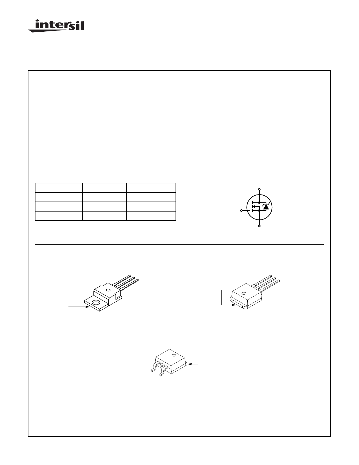
P AR T NUMBER P ACKAGE BRAND
RFP45N02L TO-220AB FP45N02L
RF1S45N02L TO-262AA F45N02L
RF1S45N02LSM TO-263AB F45N02L
NOTE: When ordering, use the entire part number. Add the suffix,
9A, to obtain the TO-263AB variant in tape and reel, e.g.
RF1S45N02LSM9A.
Packaging
JEDEC TO-220AB JEDEC TO-262AA
Description
The RFP45N02L, RF1S45N02L, and RF1S45N02LSM are
N-Channel power MOSFETs manufactured using the
MegaFET process. This process, which uses feature sizes
approaching those of LSI circuits, gives optimum utilization
of silicon, resulting in outstanding performance. They were
designed for use in applications such as switching
regulators, switching converters, motor drivers and relay
drivers. These transistors can be operated directly from integrated circuits.
Formerly developmental type TA49243.
Symbol
D
G
S
SOURCE
DRAIN
DRAIN
(FLANGE)
CAUTION: These devices are sensitive to electrostatic discharge; follow proper ESD Handling Procedures.
http://www.intersil.com or 407-727-9207
| Copyright © Intersil Corporation 1999
GATE
GATE
SOURCE
JEDEC TO-263AB
A
M
A
1
(FLANGE)
DRAIN
(FLANGE)
DRAIN
SOURCE
DRAIN
GATE
A
File Number 4342
Page 2
RFP45N02L, RF1S45N02L, RF1S45N02LSM
RFP45N02L, RF1S45N02L, RF1S45N02LSM
Absolute Maximum Ratings T
= 25oC Unless Otherwise Specified
C
RFP45N02L, RF1S45N02L,
RF1S45N02LSM UNITS
Drain to Source Voltage . . . . . . . . . . . . . . . . . . . . . . . . . . . . . . . . . . . . . . . . . . . V
Drain to Gate Voltage . . . . . . . . . . . . . . . . . . . . . . . . . . . . . . . . . . . . . . . . . . . . . V
Gate to Source Voltage . . . . . . . . . . . . . . . . . . . . . . . . . . . . . . . . . . . . . . . . . . . . V
DSS
DGR
GS
20 V
20 V
±10 V
Drain Current
Continuous . . . . . . . . . . . . . . . . . . . . . . . . . . . . . . . . . . . . . . . . . . . . . . . . . . . . . . I
Pulsed Drain Current . . . . . . . . . . . . . . . . . . . . . . . . . . . . . . . . . . . . . . . . . . . . . I
Pulsed Avalanche Rating . . . . . . . . . . . . . . . . . . . . . . . . . . . . . . . . . . . . . . . . . . . .E
Power Dissipation. . . . . . . . . . . . . . . . . . . . . . . . . . . . . . . . . . . . . . . . . . . . . . . . . . .P
DM
AS
D
Refer to Peak Current Curve
D
Derate Above 25oC. . . . . . . . . . . . . . . . . . . . . . . . . . . . . . . . . . . . . . . . . . . . . . . . . .
Operating and Storage Temperature . . . . . . . . . . . . . . . . . . . . . . . . . . . . . . .TJ,T
Soldering Temperature of Leads for 10s . . . . . . . . . . . . . . . . . . . . . . . . . . . . . . . . . T
CAUTION: Stresses above those listed in “Absolute Maximum Ratings” may cause permanent damage to the device. This is a stress only rating and operation
of the device at these or any other conditions above those indicated in the operational sections of this specification is not implied.
Electrical Specifications T
= 25oC, Unless Otherwise Specified
C
STG
L
45
Refer to UIS Curve
90
0.606
-55 to 175
260
A
W
W/oC
o
C
o
C
PARAMETER SYMBOL TEST CONDITIONS MIN TYP MAX UNITS
Drain to Source Breakdown Voltage BV
Gate to Source Threshold Voltage V
GS(TH)VGS
Zero Gate Voltage Drain Current I
Gate to Source Leakage Current I
Drain to Source On Resistance r
DS(ON)ID
Turn-On Time t
Turn-On Delay Time t
d(ON)
Rise Time t
Turn-Off Delay Time t
d(OFF)
Fall Time t
Turn-Off Time t
Total Gate Charge Q
g(TOT)VGS
Gate Charge at 5V Q
Threshold Gate Charge Q
Input Capacitance C
Output Capacitance C
Reverse Transfer Capacitance C
Thermal Resistance Junction to Case R
Thermal Resistance Junction to Ambient R
DSSID
DSS
GSS
ON
r
f
OFF
g(5)
g(TH)
ISS
OSS
RSS
θJC
θJA
= 250µA, VGS = 0V 20 - - V
= VDS, ID = 250µA1-2V
VDS = 20V,
VGS = 0V
TC = 25oC--1µA
TC = 150oC--50µA
VGS = ±10V - - ±100 nA
= 45A, VGS = 5V - - 0.022 Ω
VDD = 15V, I
RL = 0.33Ω, VGS = 5V,
RGS = 5Ω
≅ 45A,
D
- - 260 ns
-15-ns
- 160 - ns
-20-ns
-20-ns
- - 60 ns
= 0V to 10V VDD = 16V,
I
≅ 45A,
VGS = 0V to 5V - 30 36 nC
D
RL = 0.35Ω
-5060nC
VGS = 0V to 1V - 1.5 1.8 nC
VDS = 15V, VGS = 0V,
f = 1MHz
- 1300 - pF
- 724 - pF
- 250 - pF
- - 1.65
o
C/W
--80oC/W
Source to Drain Diode Specifications
PARAMETER SYMBOL TEST CONDITIONS MIN TYP MAX UNITS
Source to Drain Diode Voltage V
Reverse Recovery Time t
SD
rr
ISD = 45A - - 1.5 V
ISD = 45A, dISD/dt = 100A/µs - - 125 ns
2
Page 3
RFP45N02L, RF1S45N02L, RF1S45N02LSM
RFP45N02L, RF1S45N02L, RF1S45N02LSM
Typical Performance Curves
1.2
1.0
0.8
0.6
0.4
0.2
POWER DISSIPATION MULTIPLIER
0
0 25 50 75 100 175
TC, CASE TEMPERATURE (oC)
125
FIGURE 1. NORMALIZED POWER DISSIPATION vs
TEMPERATURE DERATING
2
1
0.5
0.2
0.1
0.1
, NORMALIZED
JC
θ
Z
THERMAL IMPEDANCE
0.01
.05
.02
.01
SINGLE PULSE
-5
10
-4
10
10
50
40
30
20
, DRAIN CURRENT (A)
D
I
10
0
150
25 50 75 100
FIGURE 2. MAXIMUM CONTINUOUS DRAIN CURRENT vs
CASE TEMPERATURE
-3
t, RECTANGULAR PULSE DURATION (s)
-2
10
125
TC, CASE TEMPERATURE (oC)
P
DM
t
1
t
NOTES:
DUTY FACTOR: D = t
PEAK TJ = PDM x R
-1
10
2
1/t2
JC
θ
0
10
x Z
θ
150
JC
+ T
175
C
1
10
FIGURE 3. NORMALIZED MAXIMUM TRANSIENT THERMAL IMPEDANCE
500
TC = 25oC, TJ = MAX RATED
100
10
, DRAIN CURRENT (A)
D
I
OPERATION IN THIS
AREA MAY BE
LIMITED BY r
1
1
VDS, DRAIN TO SOURCE VOLTAGE (V)
DS(ON)
V
DSS
MAX = 20V
10
100µs
1ms
10ms
100ms
DC
50
500
VGS = 10V
100
, PEAK CURRENT (A)
I
TRANSCONDUCTANCE
MAY LIMIT CURRENT
DM
IN THIS REGION
10
-5
10
-4
10
VGS = 5V
-3
10
10
t, PULSE WIDTH (s)
FOR TEMPERATURES
ABOVE 25
CURRENT AS FOLLOWS:
I = I
-2
o
C DERATE PEAK
175 - T
25
-1
10
FIGURE 4. FORWARD BIAS SAFE OPERATING AREA FIGURE 5. PEAK CURRENT CAPABILITY
3
150
C
TC = 25oC
0
10
1
10
Page 4

RFP45N02L, RF1S45N02L, RF1S45N02LSM
RFP45N02L, RF1S45N02L, RF1S45N02LSM
Typical Performance Curves
200
100
STARTING TJ = 150oC
10
If R = 0
, AVALANCHE CURRENT (A)
tAV = (L)(IAS)/(1.3*RATED BV
AS
I
If R ≠ 0
t
= (L/R)ln[(IAS*R)/(1.3*RATED BV
AV
1
0.001
0.01
tAV, TIME IN AVALANCHE (ms)
DSS
0.1
(Continued)
STARTING TJ = 25oC
- VDD)
) +1]
DSS-VDD
1
10
NOTE: Refer to Intersil Application Notes AN9321 and AN9322.
FIGURE 6. UNCLAMPED INDUCTIVE SWITCHING
100
VDD= 15V
75
-55oC
175oC
25oC
100
100
V
= 10V
GS
75
50
, DRAIN CURRENT (A)
25
D
I
PULSE DURATION = 250µs, TC = 25oC
0
0
1
VDS, DRAIN TO SOURCE VOLTAGE (V)
23 5
FIGURE 7. SATURATION CHARACTERISTICS
100
75
ID = 15A
ID = 30A
ID = 45A
VGS = 5V
V
= 4.5V
GS
V
= 4V
GS
VGS = 3.5V
VGS = 3V
4
50
25
, ON-STATE DRAIN CURRENT (A)
D(ON)
I
0
0
VGS, GATE TO SOURCE VOLTAGE (V)
PULSE TEST
PULSE DURATION = 250µs
DUTY CYCLE = 0.5% MAX
3.0 4.5 6.0 7.51.5
50
25
, DRAIN TO SOURCE
ON RESISTANCE (mΩ)
DS(ON)
r
0
2.5
ID = 2A
3.0
VGS, GATE TO SOURCE VOLTAGE (V)
3.5
FIGURE 8. TRANSFER CHARACTERISTICS FIGURE 9. DRAIN TO SOURCE ON RESISTANCE vs
GATE VOLTAGE AND DRAIN CURRENT
350
VDD = 15V, ID = 45A, RL = 0.333Ω
300
250
200
150
100
SWITCHING TIME (ns)
50
0
010
RGS, GATE TO SOURCE RESISTANCE (Ω)
t
r
t
f
t
d(OFF)
t
d(ON)
20
30
40
50
2.0
PULSE DURATION = 250µs, VGS = 5V, ID = 45A
1.5
1.0
0.5
NORMALIZED ON RESISTANCE
0
-80 -40 0 40 80 120 160
TJ, JUNCTION TEMPERATURE (oC)
PULSE DURATION = 250µs
4.0 4.5
5.0
200
FIGURE 10. SWITCHING TIME AS A FUNCTION OF GATE
RESISTANCE
FIGURE 11. NORMALIZED DRAIN TO SOURCE ON
RESISTANCE vs JUNCTION TEMPERATURE
4
Page 5

RFP45N02L, RF1S45N02L, RF1S45N02LSM
RFP45N02L, RF1S45N02L, RF1S45N02LSM
Typical Performance Curves
2.0
1.5
1.0
NORMALIZED GATE
0.5
THRESHOLD VOLTAGE
0
-80 -40 0 40 80 120 160
TJ, JUNCTION TEMPERATURE (oC)
(Continued)
VGS = VDS, ID = 250µA
FIGURE 12. NORMALIZED GATE THRESHOLD VOLTAGE vs
JUNCTION TEMPERATURE
2500
VGS= 0V, f = 1MHz
2000
1500
C
C
C
ISS
OSS
RSS
1000
500
C, CAPACITANCE (pF)
0
0 5 10 15 20
V
, DRAIN TO SOURCE VOLTAGE (V)
DS
2.0
ID = 250µA
1.5
1.0
0.5
BREAKDOWN VOLTAGE
NORMALIZED DRAIN TO SOURCE
200
0
-80 -40 0 40 80 120 160
T
, JUNCTION TEMPERATURE (oC)
J
FIGURE 13. NORMALIZED DRAIN TO SOURCE BREAKDOWN
VOLTAGE vs JUNCTION TEMPERATURE
20
15
10
5
, DRAIN TO SOURCE VOLTAGE (V)
0
DS
V
VDD = BV
I
GREF()
--------------------- -
20
I
GACT()
DSS
RL = 0.44Ω
= 0.5mA
I
G(REF)
V
= 5V
GS
PLATEAU VOLTAGES IN
DESCENDING ORDER:
VDD = BV
VDD = 0.75 BV
VDD = 0.50 BV
VDD = 0.25 BV
t, TIME (µs)
DSS
VDD = BV
DSS
DSS
DSS
I
GREF()
--------------------- -
80
I
GACT()
DSS
5.00
3.75
2.50
1.25
0
200
, GATE TO SOURCE VOLTAGE (V)
GS
V
FIGURE 14. CAPACITANCE vs DRAIN TO SOURCE VOLTAGE NOTE: Refer to Application Notes AN7254 and AN7260.
FIGURE 15. NORMALIZED SWITCHING WA VEFORMS FOR
CONSTANT GATE CURRENT
5
Page 6

RFP45N02L, RF1S45N02L, RF1S45N02LSM
RFP45N02L, RF1S45N02L, RF1S45N02LSM
Test Circuits and Waveforms
V
DS
t
I
AS
VARY t
TO OBTAIN
P
REQUIRED PEAK I
V
GS
AS
L
R
G
+
V
DD
-
DUT
0V
P
I
AS
t
0.01Ω
FIGURE 16. UNCLAMPED ENERGY TEST CIRCUIT FIGURE 17. UNCLAMPED ENERGY WAVEFORMS
BV
DSS
P
t
AV
V
DS
V
DD
t
ON
t
DS
d(ON)
90%
10%
t
r
R
L
V
+
V
R
G
DD
-
t
d(OFF)
t
OFF
DUT
90%
V
V
GS
GS
10%
50%
PULSE WIDTH
50%
FIGURE 18. RESISTIVE SWITCHING TEST CIRCUIT FIGURE 19. RESISTIVE SWITCHING WAVEFORMS
V
I
G(REF)
DS
R
L
V
GS
+
V
DD
-
DUT
V
DD
VGS= 1V
0
Q
g(TOT)
V
DS
Q
g(5)
V
GS
Q
g(TH)
VGS= 5V
t
f
10%
VGS= 10V
90%
I
G(REF)
0
FIGURE 20. GATE CHARGE TEST CIRCUIT FIGURE 21. GATE CHARGE WAVEFORMS
6
Page 7

RFP45N02L, RF1S45N02L, RF1S45N02LSM
RFP45N02L, RF1S45N02L, RF1S45N02LSM
Temperature Compensated PSPICE Model for the
RFP45N02L, RF1S45N02L, RF1S45N02LSM
.SUBCKT RFP45N02L 2 1 3 ; rev 11/22/94
CA 12 8 2.55e-9
CB 15 14 2.64e-9
CIN 6 8 1.05e-9
DBODY 7 5 DBDMOD
DBREAK 5 11 DBKMOD
DPLCAP 10 5 DPLCAPMOD
EBREAK 11 7 17 18 33.3
EDS 14 8 5 8 1
EGS 13 8 6 8 1
ESG 6 10 6 8 1
EVTO 20 6 18 8 1
IT 8 17 1
LDRAIN 2 5 1e-9
LGATE 1 9 4.9e-9
LSOURCE 3 7 4.9e-9
MOS1 16 6 8 8 MOSMOD M = 0.99
MOS2 16 21 8 8 MOSMOD M = 0.01
RBREAK 17 18 RBKMOD 1
RDRAIN 50 16 RDSMOD 0.14e-3
RGATE 9 20 0.89
RIN 6 8 1e9
RSCL1 5 51 RSCLMOD 1e-6
RSCL2 5 50 1e3
RSOURCE 8 7 RDSMOD 10.31e-3
RVTO 18 19 RVTOMOD 1
S1A 6 12 13 8 S1AMOD
S1B 13 12 13 8 S1BMOD
S2A 6 15 14 13 S2AMOD
S2B 13 15 14 13 S2BMOD
GATE
1
9
LGATE RGATE
ESG
EVTO
20
+
18
8
S1A
12
S1B
CA
EGS
10
-
6
8
+
-
RIN
13814
+
DPLCAP
-
6
S2A
13
S2B
13
6
8
VTO
15
EDS
+
CIN
CB
LDRAIN
DBODY
LSOURCE
SOURCE
18
RVTO
19
VBAT
+
DRAIN
2
3
5
RSCL1RSCL2
51
+
5
ESCL
51
50
RDRAIN
16
21
MOS1
14
+
5
8
--
8
DBREAK
EBREAK
MOS2
RSOURCE
11
17
+
17
18
-
7
RBREAK
IT
VBAT 8 19 DC 1
VTO 21 6 0.583
ESCL 51 50 VALUE = {(V(5,51)/ABS(V(5,51)))*(PWR(V(5,51)*1e6/176,6))}
.MODEL DBDMOD D (IS = 3.61e-13 RS = 5.06e-3 TRS1 = 3.05e-3 TRS2 = 7.57e-6 CJO = 2.0e-9 TT = 2.18e-8)
.MODEL DBKMOD D (RS = 1.66e-1 TRS1 = -2.97e-3 TRS2 = 7.57e-6)
.MODEL DPLCAPMOD D (CJO = 1.25e-9 IS = 1e-30 N = 10)
.MODEL MOSMOD NMOS (VTO = 2.313 KP = 53.82 IS = 1e-30 N = 10 TOX = 1 L = 1u W = 1u)
.MODEL RBKMOD RES (TC1 = 8.95e-4 TC2 = -1e-7)
.MODEL RDSMOD RES (TC1 = 3.82e-3 TC2 = 1.17e-5)
.MODEL RSCLMOD RES (TC1 = 2.03e-3 TC2 = 0.45e-5)
.MODEL RVTOMOD RES (TC1 = -2.27e-3 TC2 = -5.75e-7)
.MODEL S1AMOD VSWITCH (RON = 1e-5 ROFF = 0.1 VON = -4.82 VOFF= -2.82)
.MODEL S1BMOD VSWITCH (RON = 1e-5 ROFF = 0.1 VON = -2.82 VOFF= -4.82)
.MODEL S2AMOD VSWITCH (RON = 1e-5 ROFF = 0.1 VON = -2.67 VOFF= 2.33)
.MODEL S2BMOD VSWITCH (RON = 1e-5 ROFF = 0.1 VON = 2.33 VOFF= -2.67)
.ENDS
NOTE: For further discussion of the PSPICE model, consult A New PSPICE Sub-Circuit for the Power MOSFET Featuring Global
Temperature Options; written by William J. Hepp and C. Frank Wheatley.
7
Page 8

RFP45N02L, RF1S45N02L, RF1S45N02LSM
All Intersil semiconductor products are manufactured, assembled and tested under ISO9000 quality systems certification.
Intersil products are sold by description only. Intersil Corporation reserves the right to make changes in circuit design and/or specifications at any time without
notice. Accordingly, the reader is cautioned to verify that data sheets are current before placing orders. Information furnished by Intersil is believed to be accurate
and reliable. However, no responsibility is assumed by Intersil or its subsidiaries for its use; nor for any infringements of patents or other rights of third parties which
may result from its use. No license is granted by implication or otherwise under an y patent or patent rights of Intersil or its subsidiaries.
For information regarding Intersil Corporation and its products, see web site http://www.intersil.com
Sales Office Headquarters
NORTH AMERICA
Intersil Corporation
P. O. Box 883, Mail Stop 53-204
Melbourne, FL 32902
TEL: (407) 724-7000
FAX: (407) 724-7240
EUROPE
Intersil SA
Mercure Center
100, Rue de la Fusee
1130 Brussels, Belgium
TEL: (32) 2.724.2111
FAX: (32) 2.724.22.05
ASIA
Intersil (Taiwan) Ltd.
Taiwan Limited
7F-6, No. 101 Fu Hsing North Road
Taipei, Taiwan
Republic of China
TEL: (886) 2 2716 9310
FAX: (886) 2 2715 3029
8
 Loading...