

Page 1
RF1K49093
Data Sheet August 1999 File Number
2.5A, 12V, 0.130 Ohm, Logic Level, Dual
P-Channel LittleFET™ Power MOSFET
This Dual P-Channel power MOSFET is manufacturedusing
an advanced MegaFET process. This process, which uses
feature sizes approaching those of LSI integrated circuits,
gives optimum utilization of silicon, resulting in outstanding
performance. It is designed for use in applications such as
switching regulators, switching converters, motor drivers,
relay drivers, and low voltage bus switches. This product
achieves full rated conduction at a gate bias in the 3V - 5V
range, thereby facilitating true on-off power control directly
from logic level (5V) integrated circuits.
Formerly developmental type TA49093.
Ordering Information
PART NUMBER PACKAGE BRAND
RF1K49093 MS-012AA RF1K49093
NOTE: When ordering, use the entire part number. For ordering in
tape andreel, add thesuffix 96 tothe part number,i.e., RF1K4909396.
Features
• 2.5A, 12V
DS(ON)
= 0.130Ω
®
Model
•r
• Temperature Compensating PSPICE
• On-Resistance vs Gate Drive Voltage Curves
• Peak Current vs Pulse Width Curve
• UIS Rating Curve
• Related Literature
- TB334 “Guidelines for Soldering Surface Mount
Components to PC Boards”
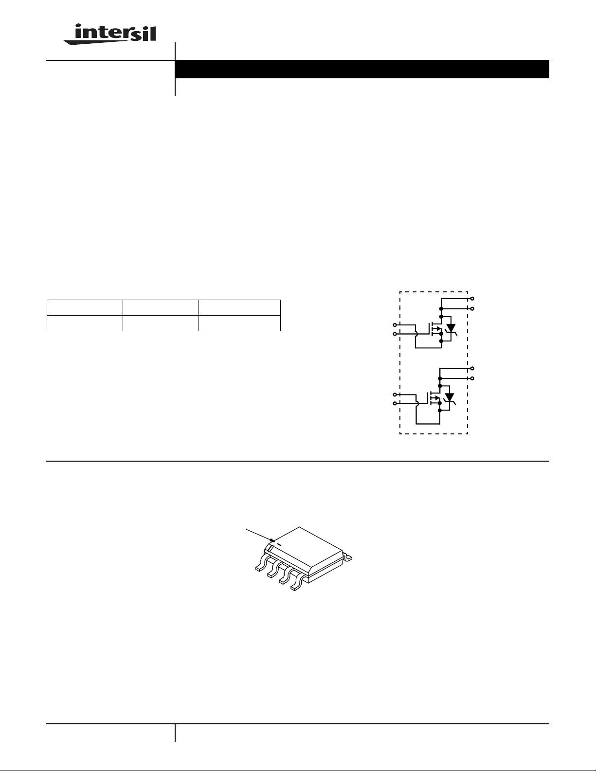
Symbol
D1 (8)
D1 (7)
S1 (1)
G1 (2)
3969.5
Packaging
JEDEC MS-012AA
BRANDING DASH
1
2
D2 (6)
D2 (5)
S2 (3)
G2 (4)
5
3
4
8-152
CAUTION: These devices are sensitive to electrostatic discharge; follow proper ESD Handling Procedures.
LittleFET™ is a trademark of Intersil Corporation. PSPICE® is a registered trademark of MicroSim Corporation.
http://www.intersil.com or 407-727-9207
| Copyright © Intersil Corporation 1999
Page 2
RF1K49093
Absolute Maximum Ratings T
= 25oC Unless Otherwise Specified
A
RF1K49093 UNITS
Drain to Source Voltage (Note 1). . . . . . . . . . . . . . . . . . . . . . . . . . . . . . . . . . . . . . . . . . V
Drain to Gate Voltage (RGS= 20kΩ, Note 1). . . . . . . . . . . . . . . . . . . . . . . . . . . . . . . . .V
Gate to Source Voltage . . . . . . . . . . . . . . . . . . . . . . . . . . . . . . . . . . . . . . . . . . . . . . . . . . V
DSS
DGR
GS
-12 V
-12 V
±10 V
Drain Current
Continuous (Pulse width = 5s) . . . . . . . . . . . . . . . . . . . . . . . . . . . . . . . . . . . . . . . . . . . . . I
Pulsed (Figure 5) . . . . . . . . . . . . . . . . . . . . . . . . . . . . . . . . . . . . . . . . . . . . . . . . . . . . . .I
Pulsed Avalanche Rating (Figure 6) . . . . . . . . . . . . . . . . . . . . . . . . . . . . . . . . . . . . . . . . E
DM
AS
D
Refer to Peak Current Curve
2.5
Refer to UIS Curve
A
Power Dissipation
TA = 25oC. . . . . . . . . . . . . . . . . . . . . . . . . . . . . . . . . . . . . . . . . . . . . . . . . . . . . . . . . . . . P
D
Derate Above 25oC . . . . . . . . . . . . . . . . . . . . . . . . . . . . . . . . . . . . . . . . . . . . . . . . . . . . . . .
Operating and Storage Temperature . . . . . . . . . . . . . . . . . . . . . . . . . . . . . . . . . . . . TJ, T
STG
Maximum Temperature for Soldering
Leads at 0.063in (1.6mm) from Case for 10s. . . . . . . . . . . . . . . . . . . . . . . . . . . . . . . . . .T
Package Body for 10s, See Techbrief 334 . . . . . . . . . . . . . . . . . . . . . . . . . . . . . . . . . . T
CAUTION: Stresses above those listed in “Absolute Maximum Ratings” may cause permanent damage to the device. This is a stress only rating and operationofthe
device at these or any other conditions above those indicated in the operational sections of this specification is not implied.
L
pkg
2
0.016
-55 to 150
300
260
W
W/oC
o
C
o
C
o
C
NOTE:
1. TJ = 25oC to 125oC.
Electrical Specifications T
= 25oC, Unless Otherwise Specified
A
PARAMETER SYMBOL TEST CONDITIONS MIN TYP MAX UNITS
Drain to Source Breakdown Voltage BV
Gate Threshold Voltage V
GS(TH)VGS
Zero Gate Voltage Drain Current I
Gate to Source Leakage Current I
Drain to Source On Resistance r
DS(ON)ID
Turn-On Time t
Turn-On Delay Time t
d(ON)
Rise Time t
Turn-Off Delay Time t
d(OFF)
Fall Time t
Turn-Off Time t
Total Gate Charge Q
g(TOT)VGS
Gate Charge at -5V Q
Threshold Gate Charge Q
Input Capacitance C
Output Capacitance C
Reverse Transfer Capacitance C
Thermal Resistance Junction-to-Ambient R
DSSID
DSS
GSS
ON
r
f
OFF
g(-5)
g(TH)
ISS
OSS
RSS
JA
θ
= 250µA, VGS = 0V, (Figure 13) -12 - - V
= VDS, ID = 250µA, (Figure 12) -1 - -2 V
VDS = -12V,
VGS = 0V
TA = 25oC---1µA
TA = 150oC - - -50 µA
VGS = ±10V - - ±100 nA
= 2.5A, VGS = -5V, (Figure 9, 11) - - 0.130 Ω
VDD = -6V, ID≈ 2.5A,
RL = 2.40Ω, VGS = -5V,
RGS = 25Ω
(Figure 10)
- - 115 ns
-25-ns
-65-ns
-40-ns
-45-ns
- - 110 ns
= 0V to -10V VDD = -9.6V,
VGS = 0V to -5V - 10 14 nC
VGS = 0V to -1V - 0.8 1.1 nC
ID = 2.5A,
RL = 3.84Ω
(Figure 15)
VDS = -10V, VGS = 0V,
f = 1MHz (Figure 14)
-1924nC
- 775 - pF
- 550 - pF
- 150 - pF
Pulse width = 1s
- - 62.5
o
C/W
Device mounted on FR-4 material
Source to Drain Diode Ratings and Specifications
PARAMETER SYMBOL TEST CONDITIONS MIN TYP MAX UNITS
Source to Drain Diode Voltage V
Reverse Recovery Time t
8-153
SD
ISD = -2.5A - - -1.25 V
ISD = -2.5A, dISD/dt = -100A/µs--55ns
rr
Page 3
Typical Performance Curves
RF1K49093
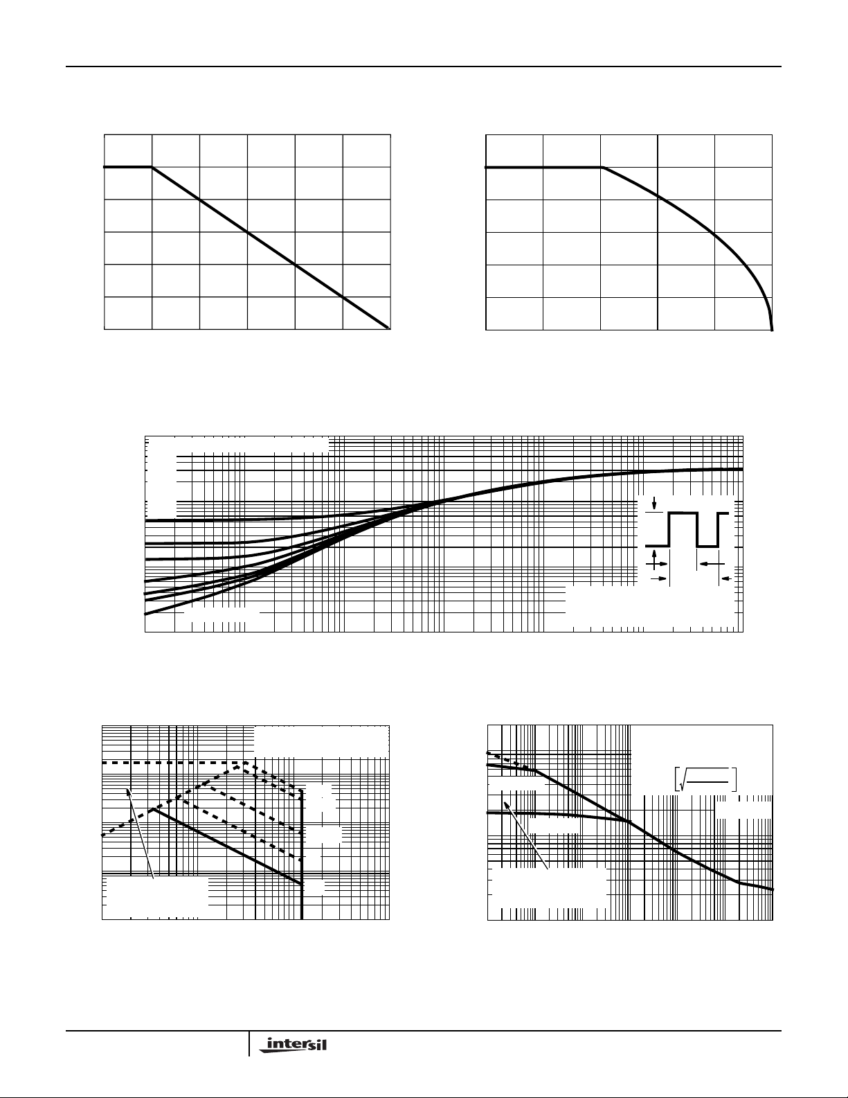
1.2
1.0
0.8
0.6
0.4
0.2
POWER DISSIPATION MULTIPLIER
0.0
0 25 50 75 100 150
TA, AMBIENT TEMPERATURE (oC)
FIGURE 1. NORMALIZED POWER DISSIPATION vs
AMBIENT TEMPERATURE
10
DUTY CYCLE - DESCENDING ORDER
0.5
0.2
0.1
0.05
0.02
1
0.01
125
-3.0
-2.5
-2.0
-1.5
-1.0
, DRAIN CURRENT (A)
D
I
-0.5
0
25 50 75 100 125 150
TA, AMBIENT TEMPERATURE (oC)
FIGURE 2. MAXIMUM CONTINUOUS DRAIN CURRENT vs
AMBIENT TEMPERATURE
P
DM
, NORMALIZED
JA
0.1
θ
Z
THERMAL IMPEDANCE
0.01
-3
10
-100
-10
-1
, DRAIN CURRENT (A)
-0.1
D
I
OPERATION IN THIS
AREA MAY BE
LIMITED BY r
-0.01
-0.1
VDS, DRAIN TO SOURCE VOLTAGE (V)
SINGLE PULSE
-2
10
-1
10
FIGURE 3. NORMALIZED MAXIMUM TRANSIENT THERMAL IMPEDANCE
TJ = MAX RATED, TA = 25oC
V
MAX = -12V
DSS
5ms
10ms
100ms
1s
DC
DS(ON)
-1 -10 -100
0
10
t, RECTANGULAR PULSE DURATION (s)
-200
-100
VGS = -10V
-10
TRANSCONDUCTANCE
MAY LIMIT CURRENT
, PEAK CURRENT CAPABILITY (A)
IN THIS REGION
DM
I
-1
-5
10
1
10
VGS = -5V
-4
10
NOTES:
DUTY FACTOR: D = t
PEAK TJ = PDM x Z
2
10
FOR TEMPERATURES
ABOVE 25
CURRENT AS FOLLOWS:
I = I
-3
10
-2
10
t, PULSE WIDTH (s)
t
1
t
2
1/t2
x R
JA
θ
θ
o
C DERATE PEAK
150 - T
25
-1
10
JA
125
+ T
A
3
10
A
TA = 25oC
0
10
1
10
FIGURE 4. FORWARD BIAS SAFE OPERATING AREA FIGURE 5. PEAK CURRENT CAPABILITY
8-154
Page 4

RF1K49093
Typical Performance Curves
-20
-10
STARTING TJ = 150oC
If R = 0
, AVALANCHE CURRENT (A)
tAV = (L)(IAS)/(1.3*RATED BV
AS
I
If R ≠ 0
= (L/R)ln[(IAS*R)/(1.3*RATED BV
t
AV
-1
0.1
tAV, TIME IN AVALANCHE (ms)
DSS
1 10 100
(Continued)
STARTING TJ = 25oC
- VDD)
- VDD) +1]
DSS
NOTE: Refer to Intersil Application Notes AN9321 and AN9322.
FIGURE 6. UNCLAMPED INDUCTIVE SWITCHING CAPABILITY
-25
-20
-15
= -6V
V
DD
-55oC
25oC
150oC
-25
= -10V
V
GS
-20
-15
-10
, DRAIN CURRENT (A)
D
I
-5
0
0
-1 -2 -3 -4 -5
VDS, DRAIN TO SOURCE VOLTAGE (V)
FIGURE 7. SATURATION CHARACTERISTICS
500
ID = -1.5A
400
ID = -2.5A
300
PULSE DURATION = 80µs
DUTY CYCLE = 0.5% MAX
V
DD
ID = -6.0A
PULSE DURATION = 80µs
DUTY CYCLE = 0.5% MAX
TA = 25oC
VGS = -5V
VGS = -4.5V
VGS = -4V
VGS = -3V
= -10V
-10
-5
, ON-STATE DRAIN CURRENT (A)
D(ON)
I
0
0.0
-1.5
VGS, GATE TO SOURCE VOLTAGE (V)
FIGURE 8. TRANSFER CHARACTERISTICS FIGURE 9. DRAIN TO SOURCE ON RESISTANCE vs GATE
120
VDD = -6V, ID = -2.5A, RL= 2.40Ω
100
80
60
40
SWITCHING TIME (ns)
20
0
10
RGS, GATE TO SOURCE RESISTANCE (Ω)
PULSE DURATION = 80µs
DUTY CYCLE = 0.5% MAX
-3.0 -4.5 -6.0
20 30 40 500
t
r
t
f
t
D(OFF)
t
D(ON)
-7.5
200
ID = -0.5A
, ON-STATE RESISTANCE (mΩ)
100
DS(ON)
r
0
-2.5 -3.5 -4.0 -4.5 -5.0
-3.0
, GATE TO SOURCE VOLTAGE (V)
V
GS
VOLTAGE AND DRAIN CURRENT
2.0
PULSE DURATION = 80µs
DUTY CYCLE = 0.5% MAX
VGS = -5V, ID = -2.5A
1.5
1.0
ON RESISTANCE
0.5
NORMALIZED DRAIN TO SOURCE
0
-80 -40 0 40 80 120 160
TJ, JUNCTION TEMPERATURE (oC)
FIGURE 10. SWITCHING TIME AS A FUNCTION OF
GATE RESISTANCE
8-155
FIGURE 11. NORMALIZED DRAIN TO SOURCE ON
RESISTANCE vs JUNCTION TEMPERATURE
Page 5

RF1K49093
Typical Performance Curves
2.0
VGS = VDS, ID = -250µA
1.5
1.0
NORMALIZED GATE
0.5
THRESHOLD VOLTAGE
0.0
-80 -40 0 40 80 120 160
TJ, JUNCTION TEMPERATURE (oC)
(Continued)
FIGURE 12. NORMALIZED GATE THRESHOLD VOLTAGE vs
JUNCTION TEMPERATURE
1200
900
600
C, CAPACITANCE (pF)
300
0
0 -2 -4 -6 -8 -10
VDS, DRAIN TO SOURCE VOLTAGE (V)
C
C
C
ISS
OSS
RSS
VGS = 0V, f = 1MHz
= CGS + C
C
ISS
C
= C
RSS
OSS
GD
= CDS + C
C
FIGURE 14. CAPACITANCE vs DRAIN TO SOURCE VOLTAGE
GD
GD
2.0
ID = -250µA
1.5
1.0
0.5
BREAKDOWN VOLTAGE
NORMALIZED DRAIN TO SOURCE
0.0
-80
-40 0 40 80 120
, JUNCTION TEMPERATURE (oC)
T
J
FIGURE 13. NORMALIZED DRAIN TO SOURCE BREAKDOWN
VOLTAGE vs JUNCTION TEMPERATURE
-12
-9
-6
-3
, DRAIN-SOURCE VOLTAGE (V)
DS
V
0
V
= BV
DD
I
G REF()
--------------------- -
20
I
G ACT()
DSS
0.75 BV
0.50 BV
0.25 BV
RL = 3.84Ω
I
= -0.5mA
G(REF)
V
= -5V
GS
t, TIME (µs)
DSS
DSS
DSS
VDD = BV
I
GREF()
--------------------- -
80
I
GACT()
DSS
-5.00
-3.75
-2.50
-1.25
0.00
NOTE: Refer to Intersil Application Notes AN7254 and AN7260.
FIGURE 15. NORMALIZED SWITCHING WAVEFORMS FOR
CONSTANT GATE CURRENT
160
, GATE-SOURCE VOLTAGE (V)
GS
V
Test Circuits and Waveforms
V
DS
VARY t
TO OBTAIN
P
REQUIRED PEAK I
0V
V
GS
t
P
AS
L
R
G
DUT
I
AS
0.01Ω
-
V
DD
+
0
V
DD
I
AS
t
P
FIGURE 16. UNCLAMPED ENERGY TEST CIRCUIT FIGURE 17. UNCLAMPED ENERGY WAVEFORMS
8-156
BV
t
AV
DSS
V
DS
Page 6

RF1K49093
Test Circuits and Waveforms
DUT
R
V
GS
FIGURE 18. SWITCHING TIME TEST CIRCUIT
12V
BATTERY
0.2µF
G
50kΩ
CURRENT
REGULATOR
0.3µF
(Continued)
R
L
-
V
DD
+
-V
DS
(ISOLATED
SUPPLY)
DUT
t
ON
t
d(ON)
t
0
V
DS
V
GS
0
10%
r
10%
90%
50%
PULSE WIDTH
t
d(OFF)
FIGURE 19. RESISTIVE SWITCHING WAVEFORMS
V
0
VGS= -1V
Q
g(TH)
90%
DS
t
OFF
90%
50%
t
f
10%
D
S
CURRENT
I
D
SAMPLING
DUT
+V
DS
G
0
I
g(REF)
IG CURRENT
SAMPLING
RESISTOR RESISTOR
FIGURE 20. GATE CHARGE TEST CIRCUIT FIGURE 21. GATE CHARGE WAVEFORMS
Soldering Precautions
The soldering process creates a considerable thermal stress
on any semiconductor component. The melting temperature
of solder is higher than the maximum rated temperature of
the device. The amount of time the device is heated to a high
temperature should be minimized to assure device reliability.
Therefore, the following precautions should always be
observed in order to minimize the thermal stress to which
the devices are subjected.
1. Always preheat the device.
2. Thedeltatemperaturebetweenthepreheatandsoldering
should alwaysbe less than 100
device can result in excessive thermal stress which can
damage the device.
o
C.Failure to preheat the
-V
GS
Q
g(-5)
V
DD
Q
0
I
g(REF)
3. The maximum temperature gradient should be less than
o
5
C per second when changing from preheating to solder-
VGS= -5V
VGS= -10V
g(TOT)
ing.
4. The peaktemperature in the soldering process should be
at least 30oC higher than the melting point of the solder
chosen.
5. The maximum soldering temperature and time must not
exceed 260oC for 10 seconds on the leads and case of
the device.
6. After soldering is complete, the deviceshould be allowed
to cool naturally for at least three minutes, as forced cooling will increase the temperature gradient and may result
in latent failure due to mechanical stress.
7. During cooling, mechanical stress or shock should be
avoided.
8-157
Page 7

PSPICE Electrical Model
SUBCKT RF1K49093 2 1 3; rev 10/24/94
CA 12 8 8.75e-10
CB 15 14 8.65e-10
CIN 6 8 7.65e-10
RF1K49093
10
DPLCAP
5
LDRAIN
2
DRAIN
DBODY 5 7 DBDMOD
DBREAK 7 11 DBKMOD
DPLCAP 10 5 DPLCAPMOD
EBREAK 5 11 17 18 -23.75
EDS 14 8 5 8 1
EGS 13 8 6 8 1
ESG 6 10 8 6 1
EVTO 20 6 8 18 1
IT 8 17 1
LDRAIN 2 5 1e-9
LGATE 1 9 1.233e-9
LSOURCE 3 7 0.452e-9
MOS1 16 6 8 8 MOSMOD M = 0.99
MOS2 16 21 8 8 MOSMOD M = 0.01
RBREAK 17 18 RBKMOD 1
RDRAIN 5 16 RDSMOD 7.36e-3
RGATE 9 20 6.1
RIN 6 8 1e9
RSOURCE 8 7 RDSMOD 4.56e-2
RVTO 18 19 RVTOMOD 1
S1A 6 12 13 8 S1AMOD
S1B 13 12 13 8 S1BMOD
S2A 6 15 14 13 S2AMOD
S2B 13 15 14 13 S2BMOD
GATE
1
LGATE RGATE
9
CA
RDRAIN
6
ESG
8
+
EVTO
+
-
13814
EGS
6
RIN
S2A
13
S2B
13
+
6
8
18
8
20
S1A
12
S1B
-
VTO
15
EDS
CIN
CB
16
+
21
MOS1
14
+
5
8
--
8
EBREAK
MOS2
DBREAK
RSOURCE
17
18
17
+
-
11
7
RBREAK
IT
DBODY
LSOURCE
SOURCE
18
RVTO
19
VBAT
+
3
VBAT 8 19 DC 1
VTO 21 6 -0.558
.MODEL DBDMOD D (IS = 3.0e-13 RS = 4.4e-2 TRS1 = 1.0e-3 TRS2 = -7.37e-6 CJO = 1.27e-9 TT = 2.2e-8)
.MODEL DBKMOD D (RS = 7.84e-2 TRS1 = -4.27e-3 TRS2 = 5.77e-5)
.MODEL DPLCAPMOD D (CJO = 2.85e-10 IS = 1e-30 N = 10)
.MODEL MOSMOD PMOS (VTO = -2.1423 KP = 9.206 IS = 1e-30 N = 10 TOX = 1 L = 1u W = 1u)
.MODEL RBKMOD RES (TC1 = 9.61e-4 TC2 = -1.09e-6)
.MODEL RDSMOD RES (TC1 = 2.10e-3 TC2 = 6.99e-6)
.MODEL RVTOMOD RES (TC1 = -1.82e-3 TC2 = 1.47e-7)
.MODEL S1AMOD VSWITCH (RON = 1e-5 ROFF = 0.1 VON = 5.47 VOFF= 3.47)
.MODEL S1BMOD VSWITCH (RON = 1e-5 ROFF = 0.1 VON = 3.47 VOFF= 5.47)
.MODEL S2AMOD VSWITCH (RON = 1e-5 ROFF = 0.1 VON = 1.05 VOFF= -3.95)
.MODEL S2BMOD VSWITCH (RON = 1e-5 ROFF = 0.1 VON = -3.95 VOFF= 1.05)
.ENDS
NOTE: For further discussion of the PSPICE model, consult A New PSPICE Sub-circuit for the Power MOSFET Featuring Global
Temperature Options; IEEE Power Electronics Specialist Conference Records, 1991.
All Intersil semiconductor products are manufactured, assembled and tested under ISO9000 quality systems certification.
Intersil semiconductor products are sold by description only.Intersil Corporation reserves the right to make changes in circuit design and/or specifications at any time without notice. Accordingly, the reader is cautioned to verify that data sheets are current before placing orders. Information furnished by Intersil is believed to be accurate and
reliable. However, no responsibility is assumed by Intersil or its subsidiaries for its use; nor for any infringements of patents or other rights of third parties which may result
from its use. No license is granted by implication or otherwise under any patent or patent rights of Intersil or its subsidiaries.
For information regarding Intersil Corporation and its products, see web site http://www.intersil.com
8-158
 Loading...