

Page 1

RF142
Heterojunction Bipolar Transistor Power Amplifier Dual-Band Controller
for GSM and PCS Applications
The RF142 Power Amplifier (PA) controller is a highly integrated, monolithic device
optimized for use in 900 MHz, 1800 MHz, and 1900 MHz Global System For
Mobile communications
®
(GSM®) and other Time Division Multiple Access (TDMA)
applications. The control current output from the RF142 can be used to control the
transmit power of a dual or multi-band Heterojunction Bipolar Transistor (HBT) PA.
The device consists of two sections: an RF detector, and a gain controller. The
RF142, when combined with a PA and a coupler, forms a closed PA control loop,
where the PA output power is controlled by a single analog reference voltage,
typically supplied by the baseband.
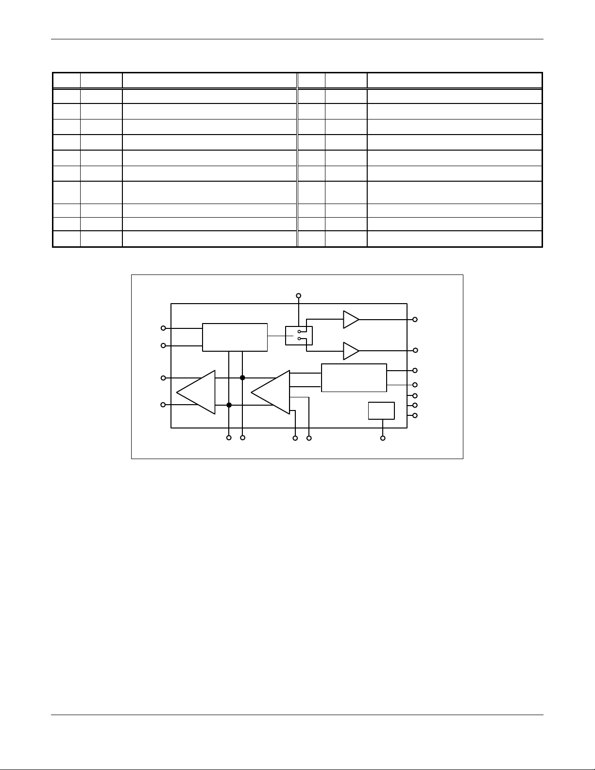
The RF142 device package and pin configuration are shown in Figure 1. The signal
pin assignments and functional pin descriptions are specified in Table 1. An RF142
block diagram is shown in Figure 2.
GND1
VREF
VMP
1
2
3
Features
• RF PA controller for use with HBT PAs
• 50 dB detector dynamic range
• Broadband, logarithmic power detector (800 MHz
to 2000 MHz)
• Logarithmic RF power detector requires no
external diodes
• Integrator and gain shaping block enhance loop
stability and linearity
• Three-cell battery operation (2.7 V to 5.0 V)
• Standby mode with 20 µA of current consumption
• 20-pin Thin Shrink Small Outline Package
(TSSOP)
Applications
• Transmit power control for dual or multi-band
GSM digital cellular handsets
20
19
18
VCC2
VPCGS M
VPCDCS
VAPC+
VAPC-
ENABLE
RFPC+
RFPC-
GND2
VCC1
4
5
6
7
8
9
10
Figure 1. RF142 Pin Configuration – 20-Pin TSSOP
17
16
15
14
13
12
11
100774A-1_090700
BAND
AUX-
AUX+
CAP-
CAP+
NC
NC
Data Sheet Conexant Doc. No. 100774B
Proprietary Information and Specifications are Subject to Change September 7, 2000
Page 2
RF142 Power Amplifier Controller
Table 1. RF142 Signal Description
Pin # Name Description Pin # Name Description
1 GND1 Ground 11 NC No connect
2 VREF Output reference voltage 12 NC No connect
3 VMP Midpoint voltage for gain shaper 13 CAP+ Integrator time constant Cap+
4 VAPC+ Tx power control positive polarity 14 CAP– Integrator time constant Cap–
5 VAPC– Tx power control negative polarity 15 AUX+ Aux output +
6 ENABLE Device enable (active high) 16 AUX– Aux output –
7 RFPC+ RF input to detector positive polarity 17 BAND
8 RFPC– RF input to detector negative polarity 18 VPCDCS 1800 MHz/1900 MHz power amplifier control voltage
9 GND2 Ground 19 VPCGSM 900 MHz power amplifier control voltage
10 VCC1 Power supply 20 VCC2 Vcc for the output stage
BAND
Band select. High selects VPCDCS as the output control
pin; low selects VPCGSM as the output control pin.
VREF
VMP
AUX+
AUX–
Gain Shaper
Amp 1
CAP-
Amp 2
CAP+
Figure 2. RF142 Block Diagram
Technical Description
The RF142 dual-band PA controller is designed to control HBT
PAs. It combines the functions of a broadband RF detector and
error amplifier/integrator to provide transmit burst control for
dual or multi-band HBT PAs. It has two separate dedicated
output stages and pins for GSM900MHz PAs and
GSM1800/1900 MHz PAs. The device, when connected to dual
or multi-band HBT PAs with a coupler, forms a loop to control
the transmit power in a dual or multi-band wireless application.
The transmit power is controlled by a single balanced analog
reference voltage input to the RF142.
The RF142 has low power consumption and operates off a
three-cell battery pack (2.7 V to 5.0 V). Extremely low standby
current of 20 µA maximizes the standby time of a GSM handset.
The absolute maximum ratings of the RF142 are provided in
Table 2, the operating conditions are specified in Table 3, and
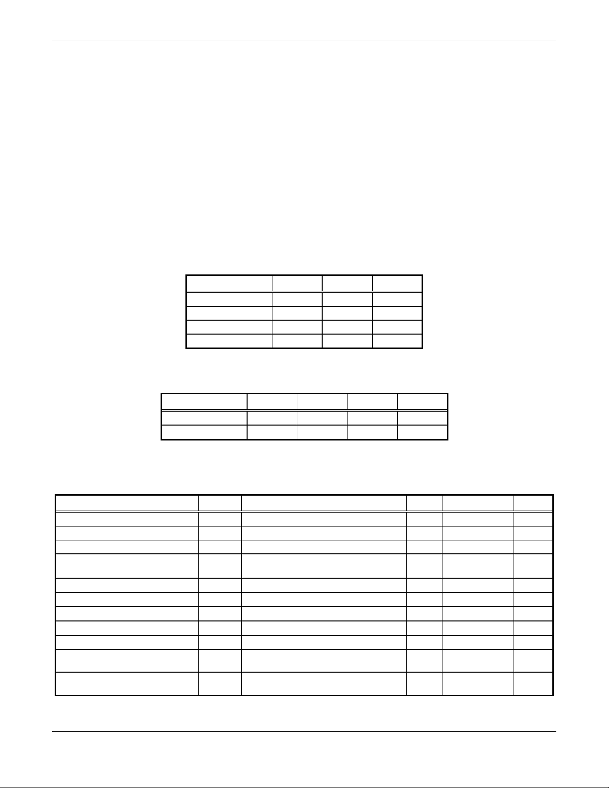
electrical specifications are provided in Table 4. Figure 3 shows
VAPC- VAPC+
the diagram for a typical application circuit using the RF142 PA
controller. Figure 4 shows the package dimensions for the 20pin TSSOP device and Figure 5 provides the tape and reel
dimensions.
RF Detector. An external RF coupler is required at the PA
output to couple the RF output from the PA to the RF logarithmic
detector input. The input to the logarithmic detector must be
within the range –40 dBm to +10 dBm. The coupled signal is fed
to the input of the RF power detector. The output from the
detector is a DC voltage that is proportional to the RF power (in
dBm) at the RFPC input to the device. The dynamic range of the
detector is 50 dB.
Integrating Error Amplifier. The integrating error amplifier
(Amp2) amplifies and integrates the voltage difference between
the detector output and the power control input, VAPC. The
integrator time constant is set by the two external capacitors
connected from AUX pins to the CAP pins.
Logarithmic
Detector
DC Bias
Circuitry
ENABLE
VPCGSM
VPCDCS
RFPC+
RFPC–
VCC2
VCC1
GND
C013
2 Conexant 100774A
September 7, 2000 Proprietary Information and Specifications are Subject to Change
Page 3
Power Amplifier Controller RF142
Gain Shaper. The output of the integrator is fed to the gain
shaping circuit that drives the gain control input of the external
RF PA. The midpoint voltage of the PA control voltage VPC, is
determined by the VMP input. The VMP input is obtained by
connecting a resistor divider to the 2.4 V reference output,
VREF. The integrator in the integrating error amplifier is used to
stabilize the loop.
The maximum voltage obtainable on VPCGSM and VPCDCS is
generally 1 V below VCC2 (pin 20). Therefore, it may be more
desirable to use a higher voltage than VCC.
Output Stages. Each of the two output stages is dedicated to a
frequency band: one for GSM900MHz and one for
GSM1800/PCS1900 MHz. The selection of the output stage is
determined by the BAND select signal. A high signal selects the
VPCDCS as the output pin and a low signal selects VPCGSM
Table 2. Absolute Maximum Ratings
Parameter Minimum Maximum Units
Storage Temperature –40 +125 °C
Supply Voltage –0.3 5.0 V
Power Dissipation -- 500 mW
Input Voltage Range –0.3 Vcc V
as the output pin. When either output is inactive, its residual
output level is extremely low to ensure that the inactive PA is
completely off.
DC Bias Block. The DC bias block provides voltage bias to the
whole chip, which may be put in standby mode using the
ENABLE digital input control pin (pin 6). The ENABLE pin is
compatible with TTL levels. When the ENABLE pin is driven
high, the device is enabled.
Electro-Static Discharge (ESD) Sensitivity
The RF142 is a static sensitive electronic device. Do not operate
or store it near strong electrostatic fields. Take proper ESD
precautions.
Table 3. RF142 Recommended Operating Conditions
Parameter Minimum Typical Maximum Units
Supply Voltage (Vcc) 2.7 3.6 4.8 V
Operating Temperature –30 +25 +85
°C
Table 4. RF142 Electrical Characteristics (1 of 2)
(TA = 25 °°°°C, Vcc = 3.6 V)
Parameter Symbol Test Condition Min Typ Max Units
Detector frequency range f 800 2000 MHz
Detector monotonic dynamic range 50 dB
Detector gain 15 mV/dB
Detector stability
Detector non-linearity error
VAPC common mode range 1.35 V
VAPC differential range
VAPC input impedance ZVAPC 20//5
VREF VREF 2.2 2.4 2.6 V
GSM Maximum Control Voltage VPCGSM
DCS Maximum Control Voltage VPCDCS
Maximum input power and over temperature range.
Minimum input power and over temperature range.
RFPC ± from –40 dBm to +8 dBm
Band <= 0.8 V
Ivpcgsm <= 75 mA
Band >= 1.90 V
Ivpcdcs <= 50 mA
±1
Vcc-1.1 Vcc-1.0 Vcc-0.9 V
Vcc-1.1 Vcc-1.0 Vcc-0.9 V
±0.5
±3
± 2
Vp-p
dB
dB
dB
kΩ//pF
100774A Conexant 3
Proprietary Information and Specifications are Subject to Change September 7, 2000
Page 4

RF142 Power Amplifier Controller
Table 4. RF142 Electrical Characteristics (2 of 2)
(TA = 25 °°°°C, Vcc = 3.6 V)
Parameter Symbol Test Condition Min Typ Max Units
GSM Maximum Sink/Source Control Current Ivpcgsm BAND <= 0.8 V 90 100 110 mA
DCS Maximum Sink/Source Control Current Ivpcdsc BAND >= 1.90 V 70 80 90 mA
VPCGSM off voltage
ENABLE = high
0.1 V
BAND = low
VPCDCS off voltage
ENABLE = high
0.1 V
BAND = high
Control output noise GSM and DCS 12
nV/√Hz
Error amplifier gain (Note) Low gain on shaper 35 40 44 dB
Auxiliary amplifier gain 25 28 31 dB
Standby current ISTDBY ENABLE = low 20
µA
Supply current ICC VPCGSM and VPCDCS source current = 0 mA 58 75 mA
BAND and ENABLE VIH VIH 1.9 V
BAND and ENABLE VIL VIL 0.8 V
Note. Included Gain Shaper
VPA
GND
FEEDBACK
TO MIXER
TXDCS
TXGSM
GND
DCSIN
GND
GSMIN
GND
VCC
DCSAPC
Dual Band
GND
PA
VCC
GSMAPC
GND
DCSOUT
GND
GSMOUT
GND
T/R
SW
DIPLEXER
T/R
SW
FILTER
TO
ANTENNA
BAND
ENABLE
VPCDCS
VPCGSM
RFPC+
RFPC-
VCC1
VCC2
GND
PAEN
PA RAMP
CONTROL
VPAC
C473
VREF
VMP
AUX+
AUX-
Amp 1
CAP-
Gain
Shaper
CAP+
Amp 2
RF142
VAPC-
Logarithmic
Detector
DC Bias
Circuitry
VAPC+
Figure 3. Typical RF142 Application Circuit
4 Conexant 100774A
September 7, 2000 Proprietary Information and Specifications are Subject to Change
Page 5

Power Amplifier Controller RF142
0.65 mm
TOP VIEW
Pin #1 indicator
6.50±0.10 mm
6.40 mm
0.24+0.06/-0.05 mm
SIDE VIEW
1.00 mm Ref
4.40±0.10 mm
END VIEW
Figure 4. RF142 Package Dimensions – 20-Pin TSSOP
1.00+0.5/-0.2 mm
1.20 mm max
0.10±0.05 mm
C003a
Pin #1
indicator
1.20
8.00 ± 0.10
4.00
6.75 ± 0.10
4.00 ± 0.10
o
8
1.50 ± 0.10
0.292 ± 0.013
Max 7o Max
1.70 ± 0.10
2.00 ± 0.05
1.50 ± 0.25
7.05 ± 0.10
Figure 5. RF142 Tape and Reel Dimensions
1.75 ± 0.10
5.50 ± 0.05
12.00 +0.30/-0.10
Notes:
1. Carrier tape material: black conductive polycarbonate
2. Cover tape material: transparent conductive PSA
3. Cover tape size: 9.3 mm width
4. Tolerance: .XX = ±0.10
5. Quantity: 2500 per reel
6. All measurements are in millimeters
C879
100774A Conexant 5
Proprietary Information and Specifications are Subject to Change September 7, 2000
Page 6

RF142 Power Amplifier Controller
Ordering Information
Model Name
Manufacturing Part
Product Revision
Number
GSM and PCS PA Controller RF142
© 2000, Conexant Systems, Inc.
All Rights Reserved.
Information in this document is provided in connection with Conexant Systems, Inc. (“Conexant”) products. These materials are provided by Conexant as a service to its
customers and may be used for informational purposes only. Conexant assumes no responsibility for errors or omissions in these materials. Conexant may make changes to
specifications and product descriptions at any time, without notice. Conexant makes no commitment to update the information and shall have no responsibility whatsoever for
conflicts or incompatibilities arising from future changes to its specifications and product descriptions.
No license, express or implied, by estoppel or otherwise, to any intellectual property rights is granted by this document. Except as provided in Conexant’s Terms and
Conditions of Sale for such products, Conexant assumes no liability whatsoever.
THESE MATERIALS ARE PROVIDED “AS IS” WITHOUT WARRANTY OF ANY KIND, EITHER EXPRESS OR IMPLIED, RELATING TO SALE AND/OR USE OF
CONEXANT PRODUCTS INCLUDING LIABILITY OR WARRANTIES RELATING TO FITNESS FOR A PARTICULAR PURPOSE, CONSEQUENTIAL OR INCIDENTAL
DAMAGES, MERCHANTABILITY, OR INFRINGEMENT OF ANY PATENT, COPYRIGHT OR OTHER INTELLECTUAL PROPERTY RIGHT. CONEXANT FURTHER DOES
NOT WARRANT THE ACCURACY OR COMPLETENESS OF THE INFORMATION, TEXT, GRAPHICS OR OTHER ITEMS CONTAINED WITHIN THESE MATERIALS.
CONEXANT SHALL NOT BE LIABLE FOR ANY SPECIAL, INDIRECT, INCIDENTAL, OR CONSEQUENTIAL DAMAGES, INCLUDING WITHOUT LIMITATION, LOST
REVENUES OR LOST PROFITS, WHICH MAY RESULT FROM THE USE OF THESE MATERIALS.
Conexant products are not intended for use in medical, lifesaving or life sustaining applications. Conexant customers using or selling Conexant products for use in such
applications do so at their own risk and agree to fully indemnify Conexant for any damages resulting from such improper use or sale.
The following are trademarks of Conexant Systems, Inc.: Conexant™, the Conexant C symbol, and “What’s Next in Communications Technologies”™. Product names or
services listed in this publication are for identification purposes only, and may be trademarks of third parties. Third-party brands and names are the property of their
respective owners.
For additional disclaimer information, please consult Conexant’s Legal Information posted at www.conexant.com, which is incorporated by reference.
Reader Response: Conexant strives to produce quality documentation and welcomes your feedback. Please send comments and suggestions to
conexant.tech.pubs@conexant.com. For technical questions, contact your local Conexant sales office or field applications engineer.
6 Conexant 100774A
September 7, 2000 Proprietary Information and Specifications are Subject to Change
Page 7

Further Information
literature@conexant.com
(800) 854-8099 (North America)
(949) 483-6996 (International)
Printed in USA
World Headquarters
Conexant Systems, Inc.
4311 Jamboree Road
Newport Beach, CA
92660-3007
Phone: (949) 483-4600
Fax 1: (949) 483-4078
Fax 2: (949) 483-4391
Americas
U.S. Northwest/
Pacific Northwest – Santa Clara
Phone: (408) 551-0270
Fax: (408) 249-7113
U.S. Southwest – Los Angeles
Phone: (949) 483-9119
Fax: (949) 483-9090
U.S. Southwest – Orange County
Phone: (949) 483-9119
Fax: (949) 483-9090
U.S. Southwest – San Diego
Phone: (858) 713-3374
Fax: (858) 713-4001
U.S. North Central – Illinois
Phone: (630) 773-3454
Fax: (630) 773-3907
U.S. South Central – Texas
Phone: (972) 733-0723
Fax: (972) 407-0639
U.S. Northeast – Massachusetts
Phone: (978) 367-3200
Fax: (978) 256-6868
U.S. Southeast – North Carolina
Phone: (919) 858-9110
Fax: (919) 858-8669
U.S. Southeast – Florida/
South America
Phone: (727) 799-8406
Fax: (727) 799-8306
U.S. Mid-Atlantic – Pennsylvania
Phone: (215) 244-6784
Fax: (215) 244-9292
Canada – Ontario
Phone: (613) 271-2358
Fax: (613) 271-2359
Europe
Europe Central – Germany
Phone: +49 89 829-1320
Fax: +49 89 834-2734
www.conexant.com
Europe North – England
Phone: +44 (0)118 920 9500
Fax: +44 (0)118 920 9595
Europe – Israel/Greece
Phone: +972 9 9524000
Fax: +972 9 9573732
Europe South – France
Phone: +33 1 41 44 36 51
Fax: +33 1 41 44 36 90
Europe Mediterranean – Italy
Phone: +39 02 93179911
Fax: +39 02 93179913
Europe – Sweden
Phone: +46 (0) 8 5091 4319
Fax: +46 (0) 8 590 041 10
Europe – Finland
Phone: +358 (0) 9 85 666 435
Fax: +358 (0) 9 85 666 220
Asia – Pacific
Taiwan
Phone: (886-2) 2-720-0282
Fax: (886-2) 2-757-6760
Australia
Phone: (613) 9583 2650
Fax: (613) 9583 9453
China – Central
Phone: 86-21-6361-2515
Fax: 86-21-6361-2516
China – South
Phone: (852) 2 827-0181
Fax: (852) 2 827-6488
China – South (Satellite)
Phone: (86) 755-518-2495
China – North
Phone: (86-10) 8529-9777
Fax: (86-10) 8529-9778
India
Phone: (91-11) 692-4789
Fax: (91-11) 692-4712
Korea
Phone: (82-2) 565-2880
Fax: (82-2) 565-1440
Korea (Satellite)
Phone: (82-53) 745-2880
Fax: (82-53) 745-1440
Singapore
Phone: (65) 737 7355
Fax: (65) 737 9077
Japan
Phone: (81-3) 5371 1520
Fax: (81-3) 5371 1501
 Loading...