

Page 1
Data Sheet
Conexant - Proprietary
Doc. No. 100777C
Data Subject to Change October 11, 2000
RF137
Transceiver For GSM Applications
The RF137 Transceiver is a highly integrated device optimized for use in singleband or multi-band Global System for Mobile Communications (GSM) applications.
In the receive path, the device consists of selectable gain Intermediate Frequency
(IF) amplifiers and an image reject downconverter with differential IF outputs.
In the transmit path, the device consists of an In-Phase and Quadrature (I/Q)
modulator and a frequency translational loop designed to perform frequency upconversion with high output spectral purity. This loop has a phase/frequency
detector, a charge-pump, a mixer, and buffers for the required isolation between
RF output, Local Oscillator (LO), and IF inputs.
In addition, the RF137 features an on-chip, dual-loop UHF/VHF frequency
synthesizer circuit. It includes two sets of reference dividers, phase/frequency
detectors, charge pumps, prescalers, main dividers, and control circuits.
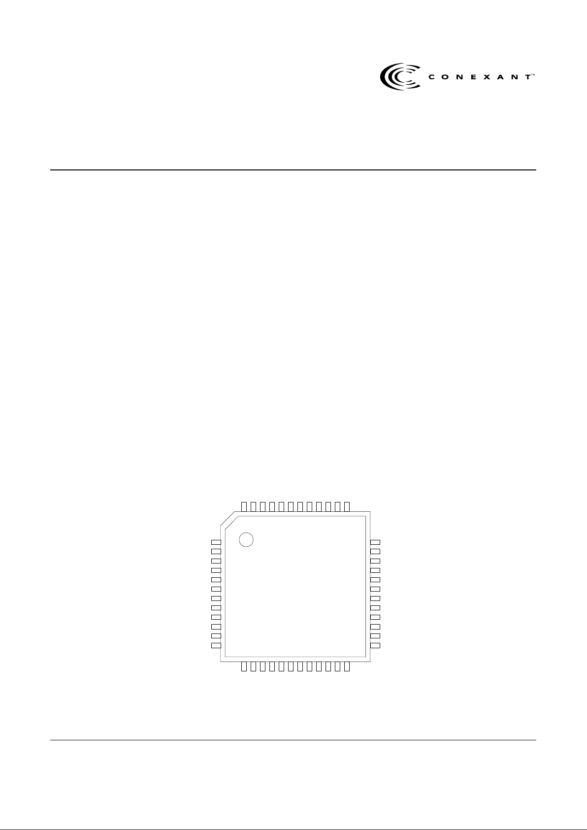
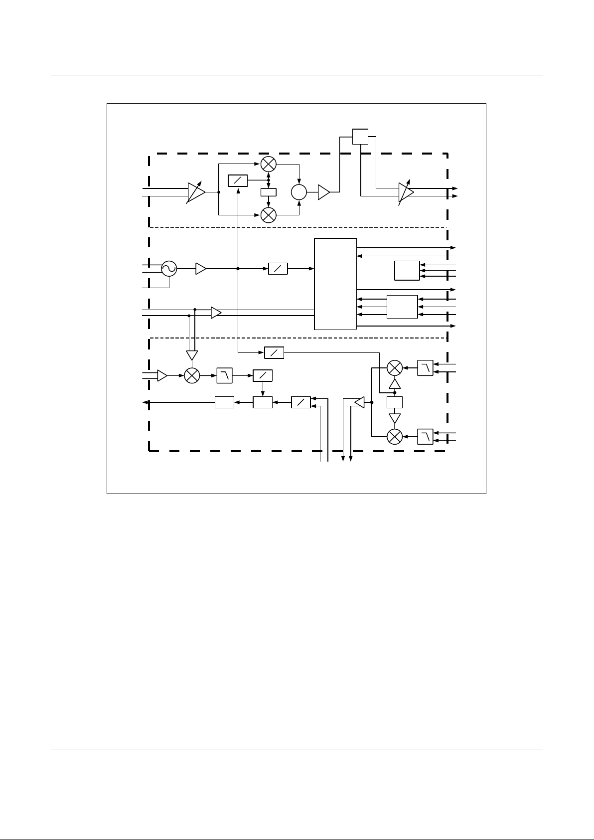
The device package and pinout of the RF137 are shown in Figure 1. A block
diagram is shown in Figure 2.
The signal pin assignments and functional pin descriptions are found in Table 1.
The absolute maximum ratings of the device are provided in Table 2, and the
operating conditions and electrical specifications are provided in Table 3.
Features
• Image-reject mixer for downconversion to 2nd IF
• 24 dB selectable attenuation on 1st IF amplifier
• 12 dB selectable attenuation on 2nd IF amplifier
• Integrated transmit path with high phase accuracy
• Reduced filtering requirements for the transmit path
• Wide RF and IF range for multi-band operation
• Integrated, fully programmable dual loop
synthesizer
• Integrated local oscillator phase shifters
• On-chip second local oscillator
• Low supply voltage down to 2.7 V
• Separate enable lines for transmit, receive, and
synthesizer modes for power management
• 48-pin Thin Quad Flat Pack (TQFP) (7mm x 7mm)
package
Applications
• GSM900/DCS1800/PCS1900 digital cellular
telephony
100777C-1_100500
GND
VCC
TLCPO
VCCB
GND
GND
TXIFIN+
TXIFIN-
TXI+
TXQ-
TXI-
TXQ+
1
2
3
4
5
6
7
8
9
10
11
12
TXMO+
CLK
TXMO-
LE
DATA
GND
VCCB
UCPO
FREF
VCCB
GND
VCPO
141516171819202122
231324
TXENA
VCC
TXRFIN+
TXRFIN-
GND
IF1IN +
LOIN+
LOIN-
IF1IN -
SXENA
RXENA
RXMXO
474645444342414039
384837
RES1
VCC
RES2
IF2IN+
IF2INIF2O+
BPC
GND
VCC
GND
LD
IF2O-
36
35
34
33
32
31
30
29
28
27
26
25
Figure 1. RF137 Pinout – 48-Pin TQFP
Page 2
RF137 Transceiver
2
Conexant - Proprietary
100777C
October 11, 2000 Data Subject to Change
C018
Bias
Rx
Sx
Rx
Sx
BPC
TLCPO
GSEL1
PFD
90˚
VHF
Synthesizer
UHF
Synthesizer
3-Wire
Control
Tx
Tx
TX LO2
90˚
Ceramic
Filter
TXQ+
TXQ-
TXI+
TXI-
TXMO+
TXMO-
CHP
IF1IN+
IF1IN-
RES1
RES2
LO1IN+
LO1IN-
TXRFIN+
TXRFIN-
TXIFIN+
TXIFIN-
RXMXO
GSEL2
RX LO2
SX LO2
÷2
÷4
RXENA
TXENA
SXENA
VCPO
FREF
UCPO
CLK
DATA
LE
LD
IF2O+
IF2O-
IF2IN+
IF2IN-
÷2
÷4
÷2
÷4
÷1
÷2
÷1
÷2
+
Figure 2. RF137 Block Diagram
Technical Description
The RF137 Transceiver consists of three main sections:
•
Receive (Rx) section
•
Transmit (Tx) section
•
Synthesizer (Sx) section
The Rx, Tx, and Sx sections can be powered up or down
independently by setting RXENA, TXENA, and SXENA high or
low.
The signal pin assignments and functional pin descriptions are
found in Table 1. Table 2 provides the absolute maximum
ratings of the RF137. The general electrical characteristics are
provided in Table 3.
Receive Section
. The receive section consists of the following
functional blocks:
•
A first IF amplifier (selectable gain step of 24 dB).
•
An image reject mixer that downconverts from a first IF to a
second IF.
•
A buffer amplifier that precedes a second IF ceramic filter.
•
A second IF amplifier (selectable gain step of 12 dB) with
differential outputs.
The first IF amplifier is a Programmable Gain Amplifier (PGA)
with selectable gains of +18 or –6 dB. The amplifier gain is
controlled by a three-wire bus. The first IF amplifier is at a high
gain state when bit S7 = 1 (Rx Gain Sel1) and CO = 1 or at a
low gain state when bit S7 = 0 (Rx Gain Sel1) and CO = 1.
The image reject mixer relaxes the first IF filtering requirements
at the image frequency of the second mixer. Image rejection is
achieved for a high side/low side injection when bit S9 is set to
the appropriate logic level and CO = 1. Table 4 defines the
three-wire bus control and output states.
Page 3
Transceiver RF137
100777C
Conexant - Proprietary
3
Data Subject to Change October 11, 2000
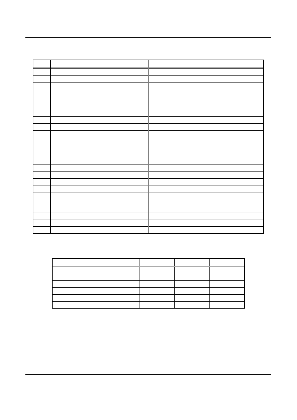
Table 1. RF137 Signal Description
Pin # Name Description Pin # Name Description
1 GND Ground 25 LD Lock detect output
2 TLCPO Translational loop c harge pump output 26 IF2O– 2nd IF output
3 VCCB Supply for synthesizers 27 IF2O+ 2nd IF output
4 VCC Supply for transceiver 28 IF2IN– 2nd IF input reference
5 GND Ground 29 IF2IN+ 2nd IF input
6 TXIFIN+ TxIF translati on loop input 30 GND Ground
7 TXIFIN– TxIF translation loop input 31 VCC Supply for transceiver
8 GND Ground 32 RES2 Resonator pin for VHF oscillator
9 TXI+ Tx modulator input 33 RES1 Resonator pin for VHF oscillat or
10 TXI– Tx modulator input 34 VCC Supply for transceiver
11 TXQ+ Tx modulator input 35 GND Ground
12 TXQ– Tx modulator input 36 BPC Bypass capacitor
13 TXMO+ Positive polari ty TX modulator output 37 SXENA Synthesizer enable
14 TXMO– Negative polarity TX modulator output 38 RXMXO Rx mixer output
15 LE Latch enable input 39 RXENA Receiver enable
16 CLK Clock input 40 IF1IN– 1st IF input
17 DATA Data input 41 IF1IN+ 1st IF input
18 VCCB Supply for synthesizers 42 LOIN– UHF local oscillator input reference
19 UCPO UHF loop charge pump output 43 LOIN+ UHF local oscillator input
20 GND Ground 44 GND Ground
21 FREF Reference input 45 VCC Supply for transceiver
22 GND Ground 46 TXRFIN– Transmit input reference
23 VCPO VHF loop charge pump output 47 TXRFIN+ Transmit input
24 VCCB Supply for synthesizers 48 TXENA Transmit enable
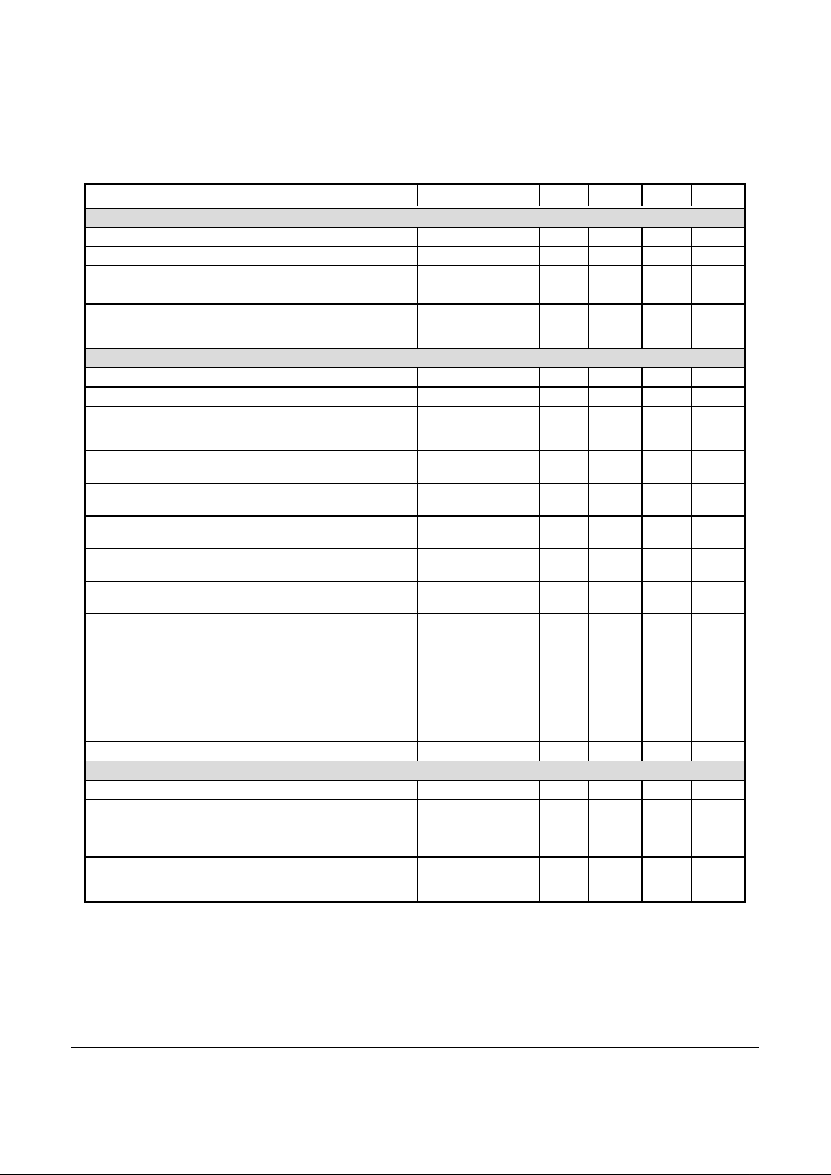
Table 2. Absolute Maximum Ratings
Parameter Minimum Maximum Units
Ambient Operating Temperature –30 +85 °C
Storage Temperature –40 +125 °C
Power Dissipation +600 mW
Supply Voltage (VCC)+4.0V
Input Voltage Range GND Vcc V
Supply Voltage (V
CCB
)4.0V
Page 4
RF137 Transceiver
4
Conexant - Proprietary
100777C
October 11, 2000 Data Subject to Change
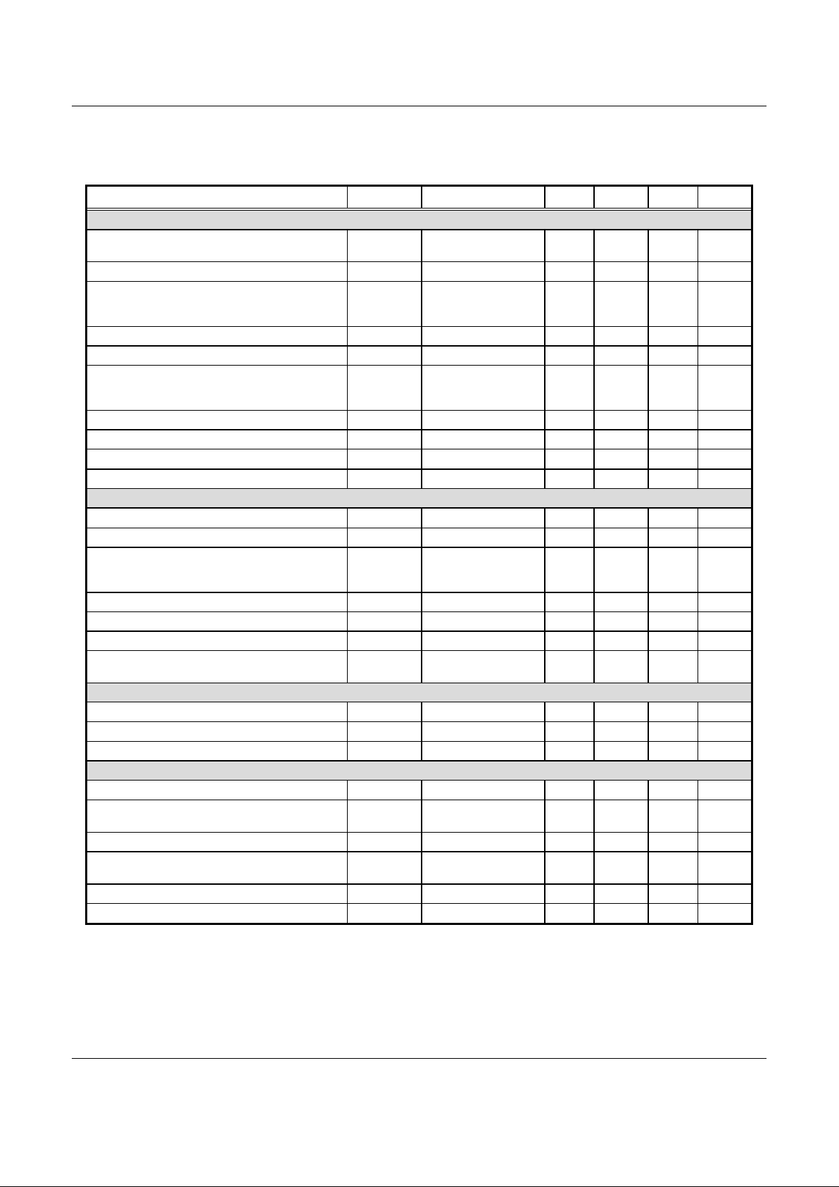
Table 3. RF137 Electrical Specifications (1 of 4)
(TA = 25
°°°°
C, Vcc = 3.0 V, except where specified)
Parameter Symbol Test Condition Min Typical Max Units
IF Amplifier/Mixer
Input impedance ZIN differential 1000//
0.5
Ω
//pF
Input operating frequenc y FN 70 450 MHz
Voltage gain:
High gain mode
Low gain mode
AV
S7 = 1, CO = 1
S7 = 0, CO = 1
+16.5
–7
+18
–6
+19
–5
dB
dB
Gain step variation dAV 0.5 dB
Single-sideband noise f igure NF High gain mode 7 8 dB
Input 1 dB compression point
High gain mode
Low gain mode
P1dB
–35
–9
–32
–7
dBV
dBV
Mixer spurious l evel Pin = –51 dBV –50 dBc
Image rejection 35 45 dB
Output impedance ZOUT 330// 2.2
Ω
//pF
Output operating frequency FOUT 14.6 MHz
2nd IF Amplifier
Input impedance ZIN 330// 2.2
Ω
//pF
Operating frequency FIF 14.6 MHz
Voltage gain:
High gain mode
Low gain mode
AV
S8 = 1, CO = 1
S8 = 0, CO = 1
17
5
18
6
19
7
dB
dB
Gain step variati on versus frequency dAV 0.5 dB
Noise figure NF 7 dB
Input P1dB P1dB low gain mode –25 –22 dBV
Output impedance ZOUT differential 1000//
1.2
Ω
//pF
Receiver
Gain temperature coefficient without ceramic f ilter 0.03 0.04
dB/°C
Power supply rejection ratio 0.5 dB/V
Input common mode rejection ratio FIN = 400 MHz 65 dB
I/Q Modulator
Input impedance ZIN differential @ 100 kHz 750// 3.3
kΩ//pF
Input common mode voltage range VCM 0.85 1.35 VCC–
1.35
V
Input offset vol tage VOS 1 5 mV
Input common mode rejecti on ratio FIN = 100 kHz
FIN = 1 MHz
75
55
dB
Output operating frequency FOUT 70 425 MHz
Output impedance ZOUT differential @400MHz 600// 3.1
Ω
//pF
Page 5
Transceiver RF137
100777C
Conexant - Proprietary
5
Data Subject to Change October 11, 2000
Table 3. RF137 Electrical Specifications (2 of 4)
(TA = 25
°°°°
C, Vcc = 3.0 V, except where specified)
Parameter Symbol Test Condition Min Typical Max Units
I/Q Modulator (conti nued)
Differential output voltage –20 –15 dBV
Output noise power NO 10 MHz offset –130 –126 dBc/Hz
LO feedthrough –43 –40 dBc
Sideband suppression 45 dB
Spurious (Note 1)
@200 kHz offset
@300 kHz offset
–60
–60
–40
–45
dBc
dBc
Translational Loop
Transmit frequency (input from VCO) fTX 800 2000 MHz
LO input frequency fLO 800 2000 MHz
IF frequency:
with divide-by- 2
with divide-by- 1
fIF
S4 = 1, CO = 1
S4 = 0, CO = 1
70
70
425
300
MHz
Transmit input power PIN
with external 50
Ω
termination
–13 –10 –7 dBm
Transmit input impedance ZIN differential 300// 0.3
Ω
pF
LO input power PIN
With external 50
Ω
termination
–13 –10 –7 dBm
LO input impedance ZIN differential 300// 0.3
Ω
pF
Tx output noise NO @ 20 MHz off set
(Note 2)
–165 –162 dBc/Hz
Charge pump output current
source/sink
source/sink
high impedance output
IOUT
S10 = 0, CO = 1
S10 = 1, CO = 1
±
1.0
±
0.5
0.02
mA
mA
mA
Tx output spurs (N ote 3):
2X spurs
3X spurs
4X spurs
5X spurs
–65
–70
–70
<–70
dBc
dBc
dBc
dBc
Device turn-on and lock time (with respect to enable input) 1 MHz loop bandwidth 30 100
µ
s
VHF VCO
Operating frequency (depends on external resonator) FVCO 300 850 MHz
Tuning voltage range:
varactor ground referenced
varactor supply referenced
0.5
VCC–
0.5
V
V
Phase noise (Note 4) 10 MHz offset, FVCO =
800 MHz, resonator Q =
20
–145 dBc/Hz
Page 6

RF137 Transceiver
6
Conexant - Proprietary
100777C
October 11, 2000 Data Subject to Change
Table 3. RF137 Electrical Specifications (3 of 4)
(TA = 25
°°°°
C, Vcc = 3.0 V, except where specified)
Parameter Symbol Test Condition Min Typical Max Units
Synthesizer
Input frequency (l ow freq. mode), VHF PLL fINL(IF) 150 260 MHz
Input frequency (hi gh freq. mode), VHF PLL fINH(IF) 250 450 MHz
Input frequency (l ow freq. mode), UHF PLL fINL(RF) 500 1200 MHz
Input frequency (hi gh freq. mode), UHF PLL fINH(RF) 500 2000 MHz
Reference frequency fREF 1 40 MHz
Reference input sensitivity RIN 500 mVpp
Phase detector frequency fPD 10 10000 kHz
Phase detector output impedance ZO 10
M
Ω
Prescaler input s ensitivity PIN 100 mVpp
Prescaler input im pedance ZIN @ 1 GHz 100
Ω
PLL contribution to phase jitter (N=11670)
Φ
NMAIN
UHF only;
Fcomparison = 100 kHz,
10 kHz loop BW;
integrated from 200 to
270,000 Hz
1.5 Degrees
RMS
Main divider phase jitter
Φ
DIV
0.5 ps
PLL contribution to phase jitter (N=1680)
Φ
NAUX
VHF only; Fcomparison =
300 kHz, 10 kHz loop BW;
integrated from 200 to
270,000 Hz
0.75 Degrees
RMS
UHF charge pump current, step 0 I
DOR,0
t=25°C
0.6 0.8 1.0 mA
UHF charge pump current, step 1 I
DOR,1
t=25°C
0.9 1.2 1.5 mA
UHF charge pump current, step 2 I
DOR,2
t=25°C
1.35 1.8 2.25 mA
UHF charge pump current, step 3 I
DOR,3
t=25°C
2.02 2.7 3.38 mA
VHF charge pump current, step 0 I
DOI,0
t=25°C
0.4 0.5 0.67 mA
VHF charge pump current, step 1 I
DOI,1
t=25°C
0.6 0.8 1.0 mA
VHF charge pump current, step 2 I
DOI,2
t=25°C
0.9 1.2 1.5 mA
VHF charge pump current, step 3 I
DOI,3
t=25°C
1.35 1.8 2.25 mA
Charge pump current relat ive step size
(current change from any one step to next step in s equence)
I
DOS
40 50 60 %
Charge pump leakage current IDOO –5 5 nA
Charge pump output voltage compl iance VDO 0.5 Vcc–0.5 V
Lock detect time constant ILOCK 500
µ
s
Lock detect phase er ror threshold 45 degrees
Three-Wire Control (refer to Figure 4)
Data to clock setup time tCS 50 ns
Data to clock hold time tCH 10 ns
Clock pulse width high tCWH 50 ns
Clock pulse width low tCWL 50 ns
Clock to load enable set up time tES 50 ns
Load enable pulse width tEW 50 ns
Load enable transition to clock start time tls 50 ns
Page 7

Transceiver RF137
100777C
Conexant - Proprietary
7
Data Subject to Change October 11, 2000
Table 3. RF137 Electrical Specifications (4 of 4)
(TA = 25
°°°°
C, Vcc = 3.0 V, except where specified)
Parameter Symbol Test Condition Min Typical Max Units
Transceiver
Enable and control VIH VIH Vcc–0.4 V
Enable and control VIL VIL 0.4 V
Enable and control IIH IIH 20 60
µ
A
Enable and control IIL IIL –10 –1 0
µ
A
Total supply current:
Rx mode
Tx mode
Synthesizer mode
Sleep mode @Vcc = 3.0V
I
CC
RXENA = SXENA = high
TXENA = SXENA = high
SXENA = high
RXENA = SXENA =
TXENA = low
48
60
27
0.04 0.2
mA
mA
mA
mA
Power supply range V
CC
(Note 5)
V
CCB
2.7
2.7
3.75
3.75
3.94
3.94
V
V
Operating temperature range T
A
–30 +25 +85
°
C
Note 1
: For 1Vp-p, 100 kHz differential signals acr oss Iin and Qin.
Note 2
: For 1 MHz loop bandwidth and external VCO with phase noise of –165 dBc/Hz @ 20 MHz offset from a carrier frequency of 900 MHz.
Note 3
: “NX spurs” denotes the order of the fLO harmonic that can mix with a harmonic of fIF and r esult in a product at zero frequency.
Note 4
: Using varactors with similar charac teristics as Loral part KV1925.
Note 5
: V
CC
must not be less than V
CCB
– 0.4 V if separate suppl y voltages are used for V
CC
and V
CCB
.
The buffer amplifier following the image reject mixer has an
output impedance of 330 Ω for direct connection to the external
ceramic filter.
The second IF amplifier converts the single-ended output from
the ceramic filter to a differential signal which may be input to a
bandpass sigma-delta A/D converter. The input impedance of
the amplifier is a nominal 330 Ω, which matches the external
ceramic filter. The nominal gain of the amplifier is 18 dB, but is
reduced to 6 dB when bit S8 = 0 (Rx Gain Sel2) and CO = 1.
Transmit Section
. The transmit section consists of the following
functional blocks:
•
A baseband to IF quadrature modulator with an output
amplifier.
•
A translation loop circuit consisting of a phase and
frequency detector, a charge pump, a TxRF input buffer, an
LO input buffer, a mixer, and a low pass filter.
The I/Q-to-IF modulator takes in differential I and Q baseband
signals. The baseband signals are initially low pass filtered and
then input to a pair of double balanced mixers. Pins 13 and 14
(TXMO+ and TXMO–, respectively), the modulator output, and
Pins 6 and 7 (TXIF+ and TXIF–, respectively), the IF input, allow
for any additional filtering required before the signals enter the
translation loop.
The translation loop circuit of the RF137, together with a VCO
and an external loop filter, forms a Phase-Locked Loop (PLL).
The inherent bandpass filtering that occurs in the PLL eliminates
the need for a duplexer or a Surface Acoustic Wave (SAW) filter
that is usually required to suppress transmission noise. The
overall efficiency is increased as a result of the elimination of
high loss, post-PA bandpass filters. This results in increased
handset talk time.
The VCO output of the translation loop is at the transmit RF
frequency. A portion of the VCO output must be fed back to Pin
47 (TXRFIN+) of the device and mixed with a buffered LO signal
to create an IF signal. The IF output from the mixer is input to
the phase and frequency detector where the IF output from the
mixer is compared with the modulated IF input to the device.
When CO = 1, the S6 bit on the three-wire bus allows for a high
side/low side injection setting.
Synthesizer Section (Sx)
. The synthesizer section consists of
the following functional blocks:
•
Frequency synthesizers
•
On-chip oscillator with external resonant circuit
•
Three-wire bus control circuit
Page 8

RF137 Transceiver
8
Conexant - Proprietary
100777C
October 11, 2000 Data Subject to Change
Table 4. RF137 Control Bits and Output States
Block C0 Bit Function Description
LO 1 S1
RX LO ÷2/÷4
Selects the division ratio for RX LO2 (0 = division ratio is 2; 1 = division ratio is 4)
S2
SX LO2 ÷2/÷4
Selects the division ratio for SX LO2 (0 = division ratio is 2; 1 = division ratio is 4)
S3
TX LO ÷2/÷4
Selects the division ratio for TX LO2 (0 = division ratio is 2; 1 = div ision ratio is 4)
TX 1 S4
TX IF ÷1/÷2
Selects the division ratio for TX IF (0 = division ratio is 1; 1 = division ratio is 2)
S5
TX MIX OUT ÷1/÷2
Selects the division ratio for TX MIX output signal (0 = division ratio is 1; 1 = division rati o is 2)
S6 TX LO Injection Selects between high-side and low-side injection of first LO input wit h respect to transmit RF (0 =
low side; 1 = high side)
Receive 1 S7 RX Gain Select 1 Selects RX 1st IF amplifier gain (0 = low gai n; 1 = high gain)
S8 RX Gain Select 2 Selects RX 2nd IF amplifier gain (0 = low gain; 1 = high gain)
S9 RX LO Injection Selects LO injection (0 = low side injection; 1 = high side injection)
TRX 1 S10 TX TL CP Current Charge pump current in translation loop c ircuit (0 = low current, 1 = high current)
S11 Reserved S11 bit may be programmed as “don’ t care.”
S12 VHF LO BUF Selects the state of LO buffer. Needs to be “1” for correct operation (0 = LO buffer off; 1 = LO
buffer on)
SX 0 S1 IF/RF Selects one of the synthesizers, either the VHF or UHF (0 = VHF is selected; 1 = UHF is selected
S2 R/N Selects the R count or N count register within the synthesizer. The N count register also controls
the phase detector current and inversion (or phase comparison reference signal) (0 = N counter
register selected; 1 = R counter register selected)
S3 S2=0: Prescaler
frequency respons e
Determines the maximum input frequency at which the prescaler will operate. S1=1 ( UHF): 0 = 1.2
GHz, 1 = 2.0 GHz; S1=0 (VHF): 0 = 260 MHz, 1 = 450 MHz
S2=1: Output invert Control s polarity of charge pump output (0 = normal operation; 1 = inverted)
S4 S2=0: Synthesizer power
down
Powers down the synthes izers. Only the synt hesizer indicated by S1 is affected (0 = Normal
operation; 1 = Power down)
S2=1: Lock detect/Test
mode select
Used to select the test mode or lock detect output on pin 25 (0 = selects the test mode output,
where S8 and S9 select the signal multiplexed to pin 25; 1 = selects the translational loop lock
detect signal for output to pin 25).
S5-
S22
S2=0: N counter This 18-bit value is loaded into the N c ounter latch. This value sets the cascaded division ratio of
the prescaler and N counter (S22=MSB, S5=LSB). For the VHF N divi der (16-bit), bits S21 and
S22 are “don’t care”.
The least significant bits (S5-S9 for UHF N divider; S5-S7 for VHF N divider) s et the prescaler
counter.
S5-S6S2=1: Output current These bits set the charge pump out put current.
S1=1 UHF: 00= 0.8, 01=1.2, 10=1.8, 11=2.7 [mA]
S1=0 VHF: 00=0.5, 01=0.8, 10=1.2, 11=1.8 [mA]
S7 S2=1: CP output
impedance
The charge pump output is changed to a high impedance output. Only the charge pump output
selected by S1 bit is affected (0 = Normal operat ion; 1 = output impedance)
S8-S9S2=1, S4 = 0: Test mode These bits select which signal is output at pi n 25 (LD) when the test mode output is selected (S2 =
1, S4 = 0).
00 = (Lock detect of VHF) AND (lock detect of UHF)
01 = Output of R divider
10 = Output of N divider
11 = Output of lock det ect VHF (S1=0) or UHF (S1=1)
S10-
S22
S2=1: R counter These 13 bits set the reference divi der value (S22=MSB, S10=LSB).
Page 9

Transceiver RF137
100777C
Conexant - Proprietary
9
Data Subject to Change October 11, 2000
There are two frequency synthesizers on the chip, one UHF and
one VHF. The UHF synthesizer can provide frequencies from
500 MHz to 2 GHz. It consists of a 32/33 modulus prescaler, a
13-bit R counter, an 18-bit N counter, a phase detector with lock
detection, and a charge pump. The VHF synthesizer, with a
frequency range from 150 MHz to 450 MHz, consists of an 8/9
modulus prescaler, a 13-bit R counter, a 16-bit N counter, a
phase detector with lock detection, and a charge pump. Each
synthesizer has four charge pump current settings for optimal
performance.
The on-chip oscillator together with a few external components
as resonant elements, form a VHF VCO (Figure 3 shows the
VCO configuration). The differential VCO output is buffered and
then fed to three dividers (Rx, Tx, Sx) with a selectable divide
ratio of either 2 or 4. The Rx and Tx dividers are both
quadrature dividers, which generates in-phase and quadrature
phase LOs.
The on-chip oscillator with the on-chip VHF synthesizer,
provides complete VHF frequency synthesis for the Rx VHF LO
and Tx VHF LO.
The three-wire bus control allows the RF137 to be optimized for
any desired frequency plan. It also programs the two on-chip
frequency synthesizers. To ensure that the data remains
latched, one of the signals TXENA, RXENA, or SXENA must
stay enabled.
When bit C0 is set to 1, it allows for divider selections in the
translation loop, high-side/low-side injection for the image reject
mixer and the receive IF amplifiers’ gain setting. When bit C0 is
set to 0, it programs the UHF/VHF synthesizer, the R/N counter,
charge pump polarity, charge pump output current, and
prescaler setting.
The three-wire bus timing diagram is provided in Figure 4.
Figure 5 illustrates a typical RF137 application circuit. Figure 6
provides the package dimensions for the 48-pin TQFP RF137
transceiver and Figure 7 provides the tape and reel dimensions.
ESD Sensitivity
Because the RF137 is a static-sensitive electronic device,
proper ESD precautions must be taken when using the RF137.
Do not operate or store the RF137 near strong electrostatic
fields.
VCC
External
Resonator
RF137
RES1
(pin 33)
RES2
(pin 32)
Vtune
C588
Figure 3. RF137 Internal VCO
Page 10

RF137 Transceiver
10
Conexant - Proprietary
100777C
October 11, 2000 Data Subject to Change
C589
Data
Clock
LE
S12/S22 S11/S21 S1 C0
tCS
tCWH
tLS
tCWL
tCH
tEW
tES
Figure 4. RF137 Wire Bus Timing Diagram
Page 11

Transceiver RF137
100777C
Conexant - Proprietary
11
Data Subject to Change October 11, 2000
LE
CLK
DATA
TXI+
2nd IF
Filter
TXI-
TXQ+
TXQ-
RXENA
TXENA
RXENA
IF2O+
IF2O-
33 pF
OUT2
OUT1
IN2
IN1
IF SAW
Filter
RXIFIN+
RXIFIN-
0.01 µF
23
16
10
33
32
31
20
21
34
3
37
29
12
39
15
44
35
8
1
22
5
30
7
6
14
13
40
41
36
43
4
24
45
27
26
47
28
RXMXO
IF2IN-
IF2IN+
IF2O-
IF2O+
TXI+
TXI-
TXQ+
TXQ-
RXENA
TXENA
SXENA
GND
GND
GND
GND
GND
GND
GND
LE
CLK
DATA
LD
VCCB
VCC
RES1
RES2
VCC
FREF
GND
VCPO
IF1IN-
IF1IN+
BPC
VCCB
VCC
TXMO+
TXMO-
TXIFIN+
TXIFIN-
VCC
LOIN
LOINR
TXRFIN+
TXRFIN-
TLCPO
38119
424846
17
25
2
TXIF filter
RF137
51 W
15 pF
TL VCO
Control
1 nF
Lock Detect
100 pF
1 kW
0.01 µF
0.01 µF
0.01 µF
270 pF
33 pF
5.6 nH
3 kW
3 kW
SMV1234-004
VHF Tune
10 W
VCCB
18
1 nF
1 nF
10 W
10 W
10 W
10 W
1 nF
VRF
0.01 µF
10 W
1.5 pF
10 nH
UCPO
19
VRF
TL VCO
14.6 MHz
2nd RXIF
1st RX IF
TO PA
1MHz Loop Bandwidth
VHF VCO
14.6 MHz RX IF output
for IF sampling at A/D
REF Freq
VSYN
2.2 kW
820 pF
820 pF
33 nF
2.2 kW
1000 pF
1.5 pF
10 nH
27 nH
18 pF
50 W
680 pF
18 nF
680 pF
2.2 kW
2.2 kW
UHF
VCO
C595
5.6 nH
1.2 µH
Figure 5. RF137 Typical Application Schematic
Page 12

RF137 Transceiver
12
Conexant - Proprietary
100777C
October 11, 2000 Data Subject to Change
DETAIL A
A1
L1
c
L
A
A2
Millimeters
0.05
8.85
0.5
0.11
1.6 MAX
0.15
9.15
5.5 REF
0.75
1.0 REF
0.500 REF
0.17
0.10 MAX
0.0020
0.3484
0.0197
0.0043
A
A1
A2
D
D1
D2
L
L1
e
b
c
Coplanarity
Min. Max. Min. Max.
Inches*
Dim.
Ref: 48-PIN TQFP (GP00-D283)
0.0630 MAX
0.006
0.3602
0.2165 REF
0.0295
0.0394 REF
0.0197 REF
0.0067
0.0039 MAX
Metric values (millimeters) should be used
for PCB layout. English values (inches) are
converted from metric values and may
contain round-off errors.
*
D1
DETAIL
A
Pin #1 indicator
e b
C004
D2
D1
D
D2D1D
1.35 1.45 0.0528 0.0571
0.2736 0.2776
6.95
7.05
0.220 REF
0.0087 REF
Figure 6. RF137 Package Dimensions – 48-Pin TQFP
Page 13

Transceiver RF137
100777C
Conexant - Proprietary
13
Data Subject to Change October 11, 2000
C880
Notes:
1. Carrier tape material: black conductive polycarbonate
2. Cover tape material: transparent conductive PSA
3. Cover tape size: 13.3mm width
4. Tolerance: .XX = ±0.10
5. Quantity: 1000 per reel
6. All measurements are in millimeters
12.00 ± 0.10
Pin #1
indicator
4.00 ± 0.10
1.50 ± 0.10
2.00 ± 0.10
1.75 ± 0.10
16.00+0.30/-0.10
1.50 ± 0.25
7.26
1.73
0.318 ± 0.013
2.46± 0.10
9.55 ± 0.10
7.09
8
o
Max 5o Max
9.45 ± 0.10
7.50 ± 0.10
Figure 7. RF137 Tape and Reel Dimensions
Page 14

RF137 Transceiver
14
Conexant - Proprietary
100777C
October 11, 2000 Data Subject to Change
Ordering Information
Model Name Manufact uring Part
Number
Product Revision
GSM Transceiver RF137
© 2000, Conexant Systems, Inc. All Rights Reserved.
Information in this document is provided in connec tion with Conexant Systems, Inc. ("Conexant") products. These materials are provided by Conexant as a service to i ts
customers and may be used f or informational purposes only. Conexant assumes no responsibility for errors or omissions in these materials. Conexant may make changes to
specificati ons and product descriptions at any time, without notice. Conexant makes no commitment to update t he information and shall have no responsibility whatsoever
for conflicts or incompatibilities arising from future changes to its specifications and product descriptions .
No license, express or implied, by estoppel or otherwise, to any intell ectual property rights is granted by this document. Except as provided in Conexant’s Terms and
Conditions of Sale for such products, Conexant assumes no liability what soever.
THESE MATERIALS ARE PROVIDED "AS IS" WITHOUT WARRANTY OF ANY KIND, EITHER EXPRESS OR IMPLI ED, RELATING TO SALE AND/OR USE OF
CONEXANT PRODUCTS INCLUDING LIABILITY OR WARRANTIES RELATING TO FITNESS FOR A PARTI CULAR PURPOSE, CONSEQUENTIAL OR INCIDENTAL
DAMAGES, MERCHANTABILITY, OR INFRINGEMENT OF ANY PATENT, COPYRIGHT OR OTHER I NTELLECTUAL PROPERTY RIGHT. CONEXANT FURTHER
DOES NOT WARRANT THE ACCURACY OR COMPLETENESS OF THE INFORMATION, TEXT, GRAPHICS OR OTHER ITEMS CONTAINED WITHIN THESE
MATERIALS. CONEXANT SHALL NOT BE LIABLE FOR ANY SPECIAL, INDIRECT, INCIDENTAL, OR CONSEQUENTIAL DAMAGES, INCLUDING WITHOUT
LIMITATION, LOST REVENUES OR LOST PROFITS, WHICH MAY RESULT FROM THE USE OF THESE MATERIALS.
Conexant products are not intended for use in medical, l ifesaving or life sustaining applications. Conexant customers using or selling Conexant products for use in such
applications do so at their own risk and agree to fully indemnify Conexant for any damages resulting from such im proper use or sale.
The following are trademarks of Conexant Systems, I nc.: Conexant™, the Conexant C symbol, and “What’s Next in Communications Technologies”™. Pr oduct names or
services listed in this publication are for identification purposes only, and may be trademark s of third parties. Third-party brands and names are the proper ty of their
respective owners.
Additional information, posted at www.conexant.com, is incorporated by reference.
Reader Response
: Conexant strives to produce quality documentation and welcomes your feedback. Please send comments and suggestions to
tech.pubs@conexant .com. For technical questions, contact your loc al Conexant sales office or field applications engineer.
Page 15

Further Information
literature@conexant.com
(800) 854-8099 (North America)
(949) 483-6996 (International)
Printed in U SA
World Headquarters
Conexant Systems, Inc.
4311 Jamboree Road
Newport Beach, CA
92660-3007
Phone: (949) 483-4600
Fax 1: (949) 483-4078
Fax 2: (949) 483-4391
Americas
U.S. Northwest/
Pacific Northwest – Santa Clara
Phone: (408) 249-9696
Fax: (408) 249-7113
U.S. Southwest – Los Angeles
Phone: (805) 376-0559
Fax: (805) 376-8180
U.S. Southwest – O range County
Phone: (949) 483-9119
Fax: (949) 483-9090
U.S. Southwest – San Diego
Phone: (858) 713-3374
Fax: (858) 713-4001
U.S. North Central – Illinois
Phone: (630) 773-3454
Fax: (630) 773-3907
U.S. South Central – Texas
Phone: (972) 733-0723
Fax: (972) 407-0639
U.S. Northeast – Massachusett s
Phone: (978) 367-3200
Fax: (978) 256-6868
U.S. Southeast – North Carolina
Phone: (919) 858-9110
Fax: (919) 858-8669
U.S. Southeast – Florida/
South America
Phone: (727) 799-8406
Fax: (727) 799-8306
U.S. Mid-Atlantic – Pennsylvania
Phone: (215) 244-6784
Fax: (215) 244-9292
Canada – Ontario
Phone: (613) 271-2358
Fax: (613) 271-2359
Europe
Europe Central – Germany
Phone: +49 89 829-1320
Fax: +49 89 834-2734
Europe North – England
Phone: +44 1344 486444
Fax: +44 1344 486555
Europe – Israel/Greece
Phone: +972 9 9524000
Fax: +972 9 9573732
Europe South – France
Phone: +33 1 41 44 36 51
Fax: +33 1 41 44 36 90
Europe Mediterranean – Italy
Phone: +39 02 93179911
Fax: +39 02 93179913
Europe – Sweden
Phone: +46 (0) 8 5091 4319
Fax: +46 (0) 8 590 041 10
Europe – Finland
Phone: +358 (0) 9 85 666 435
Fax: +358 (0) 9 85 666 220
Asia – Pacific
Taiwan
Phone: (886-2) 2-720-0282
Fax: (886-2) 2-757-6760
Australia
Phone: (61-2) 9869 4088
Fax: (61-2) 9869 4077
China – Central
Phone: 86-21-6361-2515
Fax: 86-21-6361-2516
China – South
Phone: (852) 2 827-0181
Fax: (852) 2 827-6488
China – South (Satellite)
Phone: (86) 755-518-2495
China – North
Phone: (86-10) 8529-9777
Fax: (86-10) 8529-9778
India
Phone: (91-11) 692-4789
Fax: (91-11) 692-4712
Korea
Phone: (82-2) 565-2880
Fax: (82-2) 565-1440
Korea (Satellite)
Phone: (82-53) 745-2880
Fax: (82-53) 745-1440
Singapore
Phone: (65) 737 7355
Fax: (65) 737 9077
Japan
Phone: (81-3) 5371 1520
Fax: (81-3) 5371 1501
www.conexant.com
 Loading...