

Page 1
Data Sheet
Conexant
100776A
Proprietary Information and Specifications are Subject to Change October 8, 1999
RF133
RF/IF Transceiver For GSM Applications
The RF133 RF/IF Transceiver is a highly integrated, monolithic device optimized
for use in GSM and other TDMA single-band or multi-band applications.
The receive path of the device consists of three Intermediate Frequency (IF)
amplifiers with selectable gain, an I/Q demodulator, baseband filters, DC offset
compensation circuitry, and selectable gain baseband amplifiers.
The transmit path of the device consists of an I/Q modulator and a frequency
translation loop designed to perform frequency up-conversion with high output
spectral purity. The translation loop consists of a phase/frequency detector, a
charge-pump, a mixer, and buffers for the required isolation between the RF input,
Local Oscillator (LO), and IF inputs.
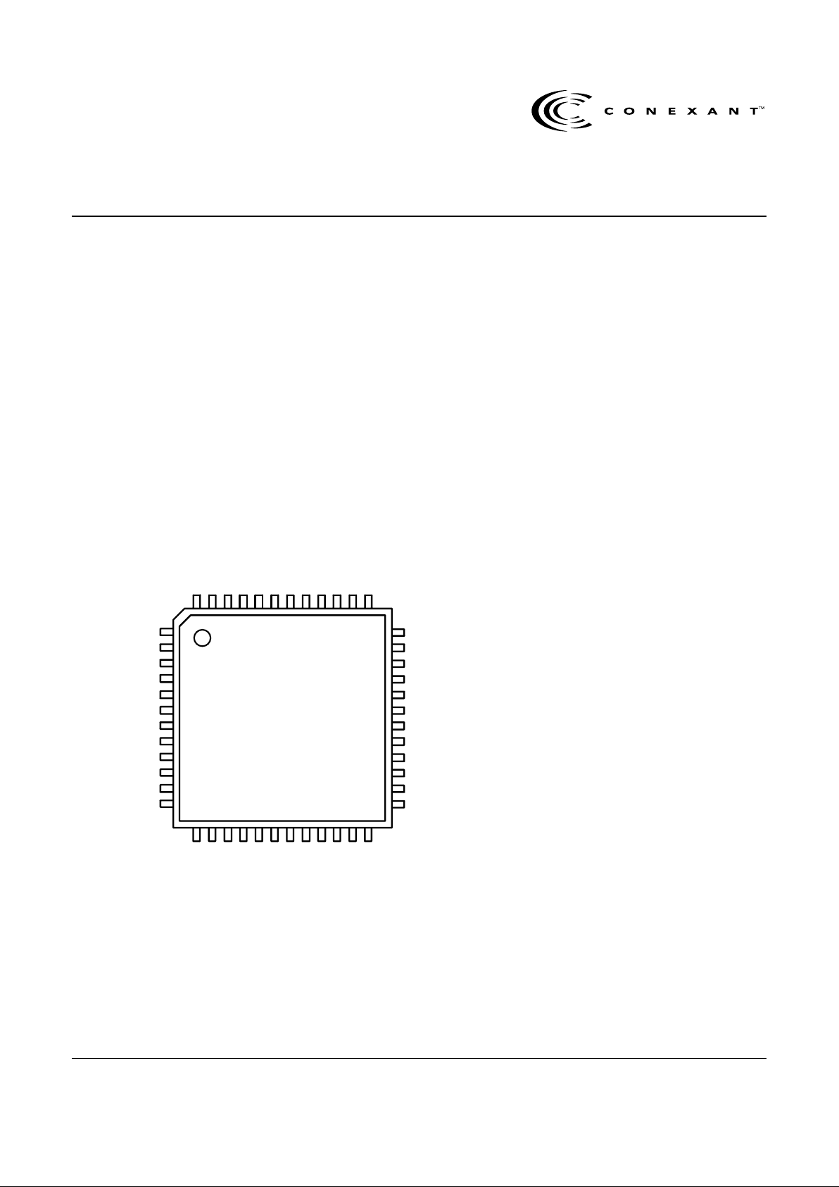
The device package and pin configuration are shown in Figure 1. A block diagram
of the RF133 is shown in Figure 2. The signal pin assignments and functional pin
descriptions are found in Table 1.
1
48 47 46 45 44 43 42 41 40 39 38 37
13 14 15 16 17 18 19 20 21 22 23 24
2
3
4
5
6
7
8
9
10
11
12
36
35
34
33
32
31
30
29
28
27
26
25
C100a
GND
TLCPO
VCC
VCC
GND
TXIFIN+
TXIFIN–
GND
TXI+
TXI–
TXQ+
TXQ–
TXMO+
TXMO–
RXI+
RXI–
RXQ+
RXQ–
T/H
CTH1
CTH2
GND
LO2O+
LO2O–
TXENA
TXRFIN+
TXRFIN–
VCC
LO1IN+
LO1IN–
GND
RFIFN+
RFIFN–
RXENALECLK
DATA
RXIFF+
RXIFF–
SXENA
BPC
GND
VCC
RES2
RES1
VCC
LPFADJ
VCC
Figure 1. RF133 Pin Configuration – 48-pin TQFP
Features
• Quadrature demodulator for downconversion
• 80 dB IF gain range and 30 dB baseband gain
range
• Integrated receive baseband filters with tunable
bandwidth
• Integrated transmit path with high phase accuracy
• Reduced filtering requirements for the transmit path
• Broad RF and IF range for multi-band operation
• Integrated selectable local oscillator dividers/phase
shifters and selectable high/low-side injection for
frequency plan flexibility
• On-chip second local oscillator
• Separate enable lines for transmit, receive, and
synthesizer modes for power management
• 48-pin Thin Quad Flat Pack (TQFP) package (7mm
x 7mm)
Applications
• GSM900/DCS1800/PCS1900 digital cellular
telephony
• Multi-mode, multi-band terminals
Page 2
RF133 RF/IF Transceiver
2
Conexant
100776A
October 8, 1999 Proprietary Information and Specifications are Subject to Change
C068
Bias
3-Wire
Control
+20 dB
0 dB –10 dB
+20 dB
+18 dB
PGA
Rx
Sx
Rx
Sx
Sx
Tx
Sx
Tx
RES1
RES2
RXIF+
RXIF–
BPC
LO1IN+
LO1IN–
TXRFIN+
TXRFIN–
TLCPO
RXI+
RXI–
RXQ+
RXQ–
CTH1
CTH2
T/H
RXENA
TXENA
SXENA
CLK
DATA
TXMO–
TXMO+
TXIFIN–
TXIFIN+
LE
LO2O+
LO2O–
TXI+
TXI–
TXQ+
TXQ–
PGB
–10 dB
DC
OC
90
˚
+20 dB
+18 dB
PGC
RXIFF+
RXIFF–
LPFADJ
PGD
0/10/20/30 dB
PFD
CHP
90
˚
÷2 ÷4
÷2 ÷4
÷2 ÷4
÷1 ÷2
÷1 ÷2
Figure 2. RF133 Block Diagram
Page 3
RF/IF Transceiver RF133
100776A
Conexant
3
Proprietary Information and Specifications are Subject to Change October 8, 1999
Table 1. RF133 Signal Descriptions
Pin # Name Description Pin # Name Description
1 GND Ground (Tx phase detector/charge pump) 25 VCC Supply (2nd LO output buffers)
2 TLCPO Translation loop char ge pump output 26 LPFADJ Adjustment pin for bas eband low pass filter corner
frequency
3 VCC Supply (phase detector and charge pump) 27 VCC Supply (2nd LO)
4 VCC Supply (Tx modulator, Rx baseband sections) 28 RES1 Resonator pin
5 GND Ground (Tx modulator, Rx baseband sections) 29 RES2 Resonator pin
6 TXIFIN+ Tx IF input 30 VCC Supply (2nd LO)
7 TXIFIN– Tx IF input 31 GND Ground (2nd LO)
8 GND Ground 32 BPC Bypass capacitor
9 TXI+ Tx modulator input 33 SXENA Synthesizer enable
10 TXI– Tx modulator input 34 RXIFF– Rx IF filter pin
11 TXQ+ Tx modulator input 35 RXIFF+ Rx IF filter pin
12 TXQ– Tx modulator input 36 DATA Data input
13 TXMO+ Tx modulator output 37 CLK Clock input
14 TXMO– Tx modulator output 38 LE Latch enable input
15 RXI+ Rx baseband output 39 RXENA Receiver enable
16 RXI– Rx baseband output 40 RXIFIN– Rx IF input
17 RXQ+ Rx baseband output 41 RXIFIN+ Rx IF input
18 RXQ– Rx baseband output 42 GND Ground (Tx mixer, Rx IF secti ons)
19 T/H Track and hold signal 43 LO1IN– 1st local oscillator input
20 CTH1 Capacitor for track and hold 44 LO1IN+ 1st local oscillator input
21 CTH2 Capacitor for track and hold 45 VCC Supply (Tx mixer, Rx IF sections)
22 GND Ground (2nd LO output buffers) 46 TXRFIN– Transmit RF input
23 LO2O+ 2nd local oscillator output 47 TXRFIN+ Transmit RF input
24 LO2O– 2nd local oscillator output 48 TXENA Transmit enable
Technical Description
The RF 133 RF/IF transceiver unit is comprised of a receive
path, a transmit path, and a synthesizer section as shown in
Figure 2. The receive path consists of a selectable gain IF
chain, a quadrature demodulator, and baseband amplifier
circuitry with I and Q outputs. The transmit path is essentially an
I/Q modulator with a translation loop for frequency upconversion. An on-chip oscillator and frequency dividers make
up the synthesizer section. Each section of the RF 133 is
separately enabled via the enable signals: TXENA, RXENA, and
SXENA.
To control different modes of operation, a serial 21-bit word (bits
S1 to S21) is written to the on-chip registers. This 21-bit word is
programmed using the three-wire input signals, CLK, DATA, and
LE. To ensure that the data remains latched, either one of the
signals TXENA, RXENA, or SXENA must stay enabled. The
operating mode that draws the least current (12 mA) is the
synthesizer mode (i.e., the mode that results when only SXENA
is enabled) (refer to Table 5). In the sleep mode, the device
typically draws less than 1 µA of current.
The block diagram in Figure 3 shows a complete RF/IF dualband transceiver chipset using the RF133.
Receive Path _______________________________________
Selectable Gain IF Chain and Quadrature Mixer. The receive
path of the RF133 is composed of an IF section and a baseband
section. The IF section consists of three programmable gain
amplifiers: PGA, PGB, and PGC.
Page 4
RF133 RF/IF Transceiver
4
Conexant
100776A
October 8, 1999 Proprietary Information and Specifications are Subject to Change
PFD
CHP
3 Wire
Control
Bias
DC
OC
PGBPGA PGC
PGD
PGD
DUAL PLL
Combiner
CTH1
CTH2
LOOP FILTER
TX DCS VCO
TX GSM VCO
TX ENA
T/H
RX ENA
SX ENA
RXI
RXQ
TXI
TXQ
CLK
DATA
LE
C453
LPF
LPF
TX IF FILTER
90
˚
90
˚
÷2 ÷4
÷2 ÷4
÷1 ÷2
÷1 ÷2
÷2 ÷4
RF210
LNA/Image Reject Mixer
IF SAW
Filter
Tx/Rx VCO
UHF VCO
GSM
Rx Filter
DCS
Rx Filter
RF133
Tx/Rx VCO
Tank
LC
Tank
Diplexer
Coupler
T/R
Antenna
RM008
RF142
VAPC
T/R
Figure 3. Dual-Band Transceiver Chipset Using The RF133
PGA has two gain settings, either 0 dB or 20 dB, whereas both
PGB and PGC have a gain range of -10 dB to 20 dB
programmable in 2 dB steps. The output of PGC is fed to a
quadrature mixer. The quadrature mixer has a fixed conversion
gain of 10 dB and its LO inputs are taken from the outputs of a
quadrature divider (divide by 2 or 4).
Baseband Integrated Filters, Baseband Amplifiers, and DC
Offset Compensation. Immediately following the quadrature
mixer (demodulator) is the baseband section (DC offset
compensation circuitry, two integrated baseband filters and two
programmable gain amplifiers). Each programmable gain
amplifier in the baseband section, both labelled PGD, has four
different gain settings: 0 dB, 10 dB, 20 dB, or 30 dB.
The corner frequency of the integrated baseband filters is
adjustable by using an appropriate value resistor at pin 26,
LPFADJ. At the nominal cutoff frequency of 105 kHz, the
resistor value is 75.1 kΩ.
Due to possible high gain of the baseband amplifiers (PGD), any
DC offsets at the outputs of the quadrature mixer are amplified
and, if uncorrected, the I and Q outputs can suffer from
significant unwanted DC offset voltages. To cancel out these
effects, the RF133 must be calibrated.
During compensation, the correction voltages are stored in
external hold capacitors CTH1 and CTH2, then the loop is
opened immediately thereafter. The corrected I and Q outputs
are then fed directly to external circuitry for further baseband
processing.
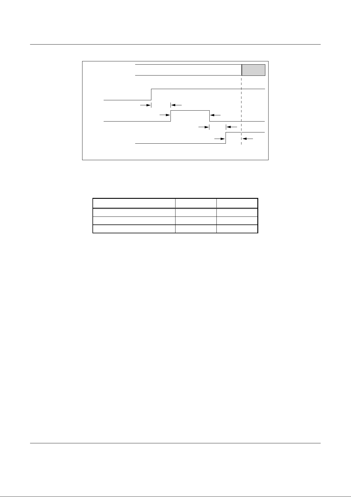
The timing diagram for this calibration sequence in reference to
the receive slot is shown in Figure 4 (the front-end mixer is
assumed to be Rockwell’s RF210 dual-band, image reject
downconverter). At first, the RF133 receiver is turned on
(RXENA is high). After time T1, the track and hold signal, T/H,
places the DC compensation circuitry in the track mode for time
T2. Then, there is a settling time, T3, before the external frontend is turned on. Finally, the front-end must be turned on for
time T4 before the receive slot.
Time T2 can vary from 10 µsec to 350 µsec. This duration is
dependent on 1) the value of the hold capacitors (CTH1 and
CTH2), and 2) whether the calibration is done from frame to
frame or from a cold start. This is tabulated in Table 2.
Page 5
RF/IF Transceiver RF133
100776A
Conexant
5
Proprietary Information and Specifications are Subject to Change October 8, 1999
T1
Rx slot
RXENA
T/H
Front-end
enable
(external to RF133)
TDMA slots
T2
T3
T4
C064
Figure 4. RF133 Sample and Hold Timing Diagram
Table 2. Minimum Required DC Offset Calibration Time T2 a nd Droop Rate
Hold Capacitor (CTH1, CTH2) 22 nF 120 nF
Cold start 60 µsec 350 µs
Frame-to-frame 10 µsec 60 µs
Typical droop-rat e (@ I/Q outputs) 1 mV/msec 0.17 mV/m s
Because of on-chip loading currents, the hold capacitors (CTH1
and CTH2) slowly discharge causing the I and Q DC offset
voltages to droop if the RF133 remains uncalibrated for an
extended period of time (the droop rate versus the hold
capacitor is also shown in Table 2).
To rectify this voltage droop, it is recommended that
recalibration occur before every receive slot (i.e., every 4.6 ms
for GSM).
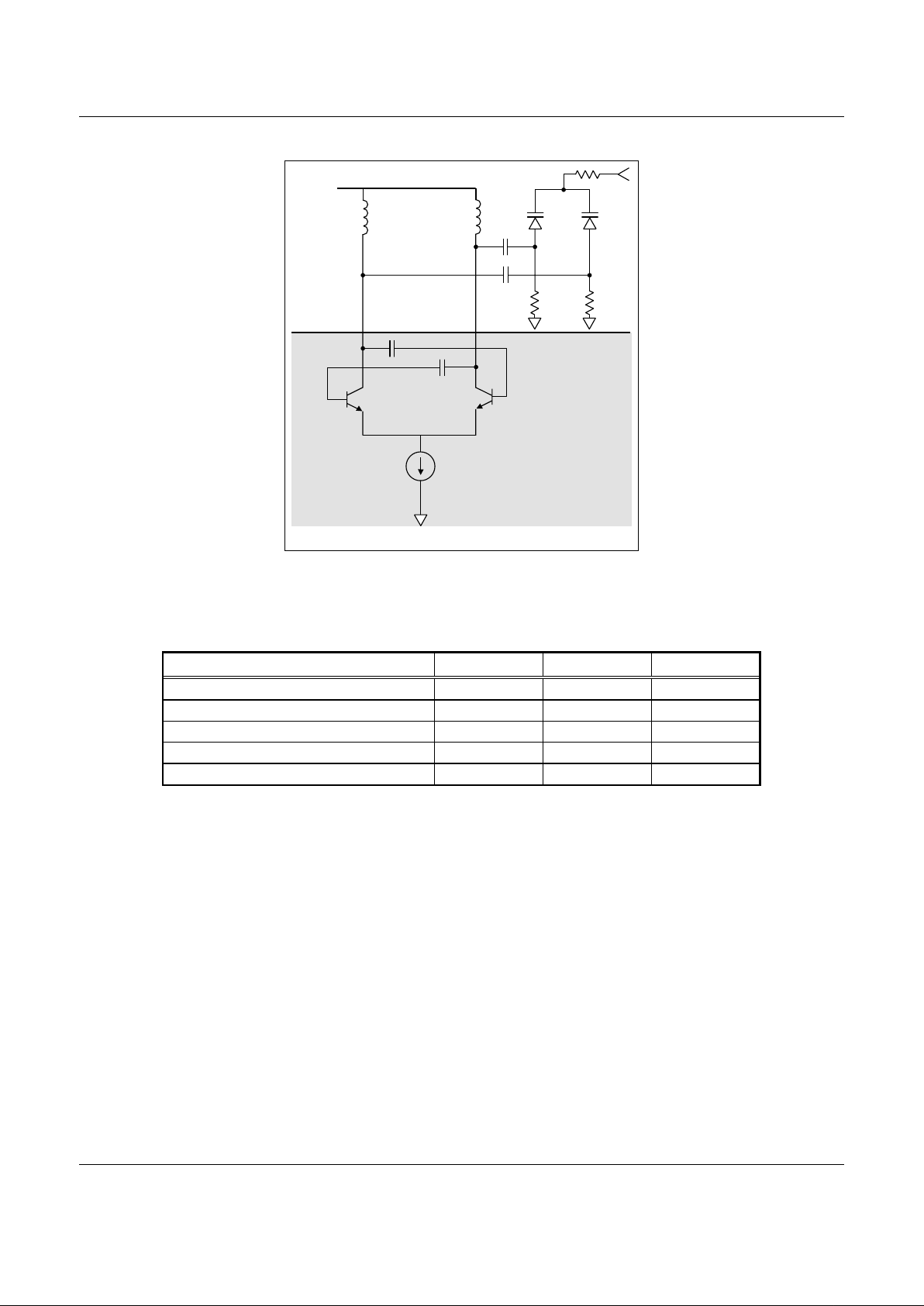
Internal Voltage Controlled Oscillator (VCO) and Frequency
Dividers. The differential VCO output is buffered and then fed to
three frequency dividers (Rx, Tx, PLL) with a selectable divide
ratio of either 2 or 4. The Rx and Tx dividers are both
quadrature dividers, which generate in-phase and quadrature
LOs. The buffered PLL divider output can be used to drive an
external PLL IC. The resonant element of the VCO is connected
to pins 28 (RES1) and 29 (RES2). Figure 5 shows the VCO
configuration.
Transmit Path_______________________________________
The transmit path consists of the following functional blocks:
•
An I/Q modulator with IF output amplifier.
•
A translation loop circuit consisting of a phase/frequency
detector, a charge pump, a Tx RF input buffer, an LO input
buffer, a mixer, two dividers, and a low pass filter.
The inputs to the I/Q modulator are differential I and Q
baseband signals which are low-pass filtered and then applied
to a pair of double balanced mixers (see Figure 2). The outputs
of the mixers are combined to produce a modulated signal
which is then filtered externally and input through pins 6 and 7
(TXIFIN+ and TXIFIN-) to the reference divider in the translation
loop.
The translation loop circuit together with the external transmit
VCO, external LO, and loop filter, form a PLL with a mixer in the
feedback loop. This PLL upconverts the modulated IF signal to
the transmit frequency which then drives the final power
amplifier. Since inherent bandpass filtering occurs in the PLL,
the need for a post PA duplexer is removed. This is the major
advantage a translation loop approach has over the
conventional upconversion scheme. The elimination of this
duplexer reduces the loss in the transmit path which in turn
reduces the output level of the final power amplifier and,
therefore, reduces the current consumption. Immediate benefits
of this approach are increased handset talk time and standby
time, and less component count.
Page 6
RF133 RF/IF Transceiver
6
Conexant
100776A
October 8, 1999 Proprietary Information and Specifications are Subject to Change
VCC
External
Resonator
RF133
RES1
(pin 28)
RES2
(pin 29)
Vtune
C321
Figure 5. RF133 Internal VCO
Table 3. Absolute Maximum Ratings
Parameter Minimum Maximum Units
Ambient Operating Temperature –40 +85 °C
Storage Temperature –50 +125 °C
Power Dissipation 600 mW
Supply Voltage (VCC) 0 +5 V
Input Voltage Range GND VCC V
The charge pump current can be programmed to be either 1 mA
or 0.5 mA and the translation loop can also be programmed to
allow for high side or low side injection of the first LO input with
respect to the transmit RF.
Even greater flexibility in the transceiver frequency planning is
possible because of the programmable dividers in the feedback
and the reference paths.
The absolute maximum ratings of the RF133 are provided in
Table 3, and the electrical specifications are provided in Table 4.
Tables 5, 6, and 7 detail the setting of the programmable
operation modes. Figure 6 illustrates the timing of the three-wire
bus control signal and Figure 7 provides a graph of the input
compression versus the receiver gain.
Figure 8 shows a typical application circuit diagram. Figure 9
provides the package dimensions for the 48-pin device.
Page 7

RF/IF Transceiver RF133
100776A
Conexant
7
Proprietary Information and Specifications are Subject to Change October 8, 1999
Table 4. RF133 Electrical Specifications (1 of 4)
(Ta = 25 °°°°C, VCC = 3.0 V, except where noted)
Parameter Symbol Test Condition Min Typ Max Units
Receive IF Path
Input impedance Z
IN
Differential 1k//
0.15
Ω
pF
Input operating frequenc y F
IN
70 450 MHz
Voltage gain
A
V
A
V
FIN = 400 MHz
High gain mode
Low gain mode
57
–23
60
–20
63
–17
dB
dB
Gain step (Note 1) dA
V
2dB
Gain step accuracy (Note 2) –0.5 +0.5 dB
Single-sideband noise f igure NF
NF
High gain mode
Low gain mode
7
23
dB
dB
Input 1 dB compression point (Note 3) P
1dB
P
1dB
High gain mode (60 dB)
Low gain mode
(–20 dB)
–75
–12
dBV
dBV
IF filter pin impedance Z
IF
Differential 600//
1
Ω
pF
I/Q Demodulator
Voltage gain (Quadrature mixer) A
V
10 dB
I/Q amplitude imbalanc e 1dB
I/Q phase imbalance –3 +3 degrees
Noise Figure NF 15 dB
Output 1 dB compression poi nt –2 dBV
Baseband Filter
Corner frequency (pr ogrammable) F
C
50 150 kHz
Corner frequency variation dF
C
–15 +15 %
Rejection FC = 105 kHz:
@200 kHz
@400 kHz
@600 kHz
26
8
30
40
dB
dB
dB
Group delay FC = 105 kHz:
DC to 100 kHz 3 5
µs
Group delay variation FC = 105 kHz:
DC to 100 kHz 300 500 ns
Baseband Amplifier
Voltage gain A
V
0
10
20
30
dB
dB
dB
dB
Page 8

RF133 RF/IF Transceiver
8
Conexant
100776A
October 8, 1999 Proprietary Information and Specifications are Subject to Change
Table 4. RF133 Electrical Specifications (2 of 4)
(TA = 25 °°°°C, VCC = 3.0 V, except where noted)
Parameter Symbol Test Condition Min Typ Max Units
Baseband Amplifier (continued)
Output amplitude AV = 30 dB
Av = 20 dB
Av = 10 dB
A
V
= 0 dB
2.5
1.8
1.0
0.4
Vp-p
Vp-p
Vp-p
Vp-p
Output common mode voltage 1.35 V
Output offset voltage With DC offset
compensation
Without DC offset
compensation and AV = 0
dB
±5
±100
mV
mV
Output voltage droop/rise rate With DC offset
compensation, C
TH
= 22 nF
1mV/ ms
Output impedance Z
OUT
Differential 200
Ω
I/Q Modulator
Input impedance Z
IN
Differential 20
kΩ
Input common mode voltage range V
CM
0.85 1.35 VCC –
1.35
V
Input offset voltage V
OS
15mV
Input frequency 3 dB bandwidth 10 MHz
Input common mode rejection ratio FIN = 100 kHz
F
IN
= 1 MHz
75
55
dB
dB
Output operating frequenc y F
OUT
70 450 MHz
Output impedance Z
OUT
Differential 800
Ω
Output voltage V
OUT
–20 –15 dBV
Output noise power N
O
10 MHz offset –130 –126 dBc/Hz
LO feedthrough –45 –40 dBc
Sideband suppression 40 50 dBc
Spurious (Note 4) @ 200 kHz offset
@ 300 kHz offset
–70
–60
–40
–45
dBc
dBc
Translation Loop
Transmit frequency (input from VCO) f
TX
800 2000 MHz
LO input frequency f
LO
800 2000 MHz
IF frequency f
IF
f
IF
With divide-by-2
With divide-by-1
70
70
425
300
MHz
MHz
Transmit input power P
IN
With external 50 Ω
termination
–13 -10 –7 dBm
Transmit input impedance (at pin 47) Z
IN
With pin 46 AC grounded 300//
0.3
Ω
pF
LO input power with external 50 Ω termination
P
IN
–13 -10 –7 dBm
LO input impedance (at pin 44) Z
IN
With pin 43 AC grounded 300//
0.3
Ω
pF
Page 9

RF/IF Transceiver RF133
100776A
Conexant
9
Proprietary Information and Specifications are Subject to Change October 8, 1999
Table 4. RF133 Electrical Specifications (3 of 4)
(TA = 25 °°°°C, VCC = 3.0 V, except where noted)
Parameter Symbol Test Condition Min Typ Max Units
Translation Loop (continued)
Charge-pump output current I
OUT
Source/sink (CPOI =
HIGH)
Source/sink (CPOI =
LOW)
High impedance input
±1.0
±0.5
0.02
mA
mA
mA
Transmit output zer o crossing spurs:
2X spurs
3X spurs
4X spurs
5X spurs
–62 –65
–70
–70
< –70
dBc
dBc
dBc
dBc
Transmit output nois e level (Note 5) At 20 MHz offset fr om
carrier
–165 –162 dBc/Hz
Device turn-on and lock time (with respect to enable input) 30 100
µs
VCO
Operating frequency set by resonator F
VCO
300 900 MHz
Tuning voltage range Varactor ground
referenced
Varactor supply
referenced
0.3
VCC–
0.3
V
V
Resonator pin impedance Differential 10k//
0.4
Ω
pF
Tuning sensitivity (Note 6) K
VCO
FVCO = 800 MHz 50 MHz/ V
LO phase noise at 10 MHz offset (Note 6) FVCO = 800 MHz
Q = 20
–122 dBc/Hz
Second LO output level Unloaded, per side 260 mVp
Second LO output impedance Di fferential 200
Ω
3-Wire Control
Data to clock setup time (Note 7) t
CS
50 ns
Data to clock hold time (Note 7) t
CH
10 ns
Clock pulse width hi gh (Note 7) t
CWH
50 ns
Clock pulse width l ow (Note 7) t
CWL
50 ns
Clock to load enable setup time (Note 7) t
ES
50 ns
Load enable pulse width (Note 7) t
EW
50 ns
Page 10

RF133 RF/IF Transceiver
10
Conexant
100776A
October 8, 1999 Proprietary Information and Specifications are Subject to Change
Table 4. RF133 Electrical Specifications (4 of 4)
(TA = 25 °°°°C, VCC = 3.0 V, except where noted)
Parameter Symbol Test Condition Min Typ Max Units
Transceiver
DC offset calibr ation timing (see Figure 4):
T1
T2 (see Table 2)
T3
T4 (assuming RF210 front- end mixer)
40
5
20
µs
µs
µs
µs
Enable and control VIH V
IH
VCC ×
0.8
V
Enable and control VIL V
IL
VCC ×
0.2
V
Enable and control IIH I
IH
20 60
µA
Enable and control IIL I
IL
–10 –1 0
µA
Total supply current:
Rx mode
Tx mode
Synthesizer mode
Sleep mode (V
CC
= 5.0 V)
I
CC
(SXENA=RXENA=on)
(SXENA=TXENA=on)
(SXENA=on)
52
54
17
0.1
mA
mA
mA
mA
Power supply range (tr ansceiver Vcc) VCC 2.7 3.0 5.0 V
Operating temperature range T
A
–40 +25 +85
°C
Note 1: Gain steps are such that monotonicit y is maintained throughout the entire IF gain range.
Note 2: Specified down to 2.8 V supply voltage. Slight degradation at temperature extremes for 2.7 V supply voltage.
Note 3: Refer to Figure 7 for the 1 dB compression point of the entire recei ver chain, including the baseband gain section.
Note 4: For 1 Vp-p 100 kHz dif ferential signals acorss lin and Qin.
Note 5: Using transmit VCO with similar char acteristics as Murata MQE 550-902.
Note 6: Using varact ors with similar characteristics as Alpha part SMV1234-004.
Note 7: Refer to Figure 6.
Page 11

RF/IF Transceiver RF133
100776A
Conexant
11
Proprietary Information and Specifications are Subject to Change October 8, 1999
Table 5. RF133 Control Bits and Output States
Block C0 Bit State 1 0
LO 1 S1
S2
S3
RX LO ÷2/÷4
2ND LO ÷2/÷4
TX LO ÷2/÷4
divide by 4
divide by 4
divide by 4
divide by 2
divide by 2
divide by 2
TL 1 S4
S5
S6
S7
TX IF ÷1/÷2
TX MIX OUT ÷1/÷2
TX LO INJECTION
CP OUTPUT CURRENT
divide by 2
divide by 2
High Side
1 mA
divide by 1
divide by 1
Low Side
0.5 mA
Receive 1 S8
S9
S10
S11
S12
S13
S14
S15
S16
S17
S18
RX PGA1
RX PGB1
RX PGB2
RX PGB3
RX PGB4
RX PGC1
RX PGC2
RX PGC3
RX PGC4
RX PGD1
RX PGD2
(see Table 6)
(see Table 6)
(see Table 6)
(see Table 6)
(see Table 6)
(see Table 6)
(see Table 6)
(see Table 6)
(see Table 6)
(see Table 7)
(see Table 7)
TRX 1 S19 TRX BAND High Band Low Band
1 S20 Reserved
1 S21 LO BUFFER ON/OFF ON OFF
Page 12

RF133 RF/IF Transceiver
12
Conexant
100776A
October 8, 1999 Proprietary Information and Specifications are Subject to Change
Table 6. Receive IF Gain
Gain
(dB)
PGA PGB PGC
112341234
60 111111111
58 111101111
56 111011111
54 111001111
52 110111111
50 110101111
48 110011111
46 110001111
44 101111111
42 101101111
40 101011111
38 101001111
36 100111111
34 100101111
32 100011111
30 100001111
28 010011111
26 010001111
24 001111111
22 001101111
20 001011111
18 001001111
16 000111111
14 000101111
12 000011111
10 000001111
8 000001110
6 000001101
4 000001100
2 000001011
0 000001010
–2 000001001
–4 000001000
–6 000000111
–8 000000110
–10000000101
–12000000100
–14000000011
–16000000010
–18000000001
–20000000000
Page 13

RF/IF Transceiver RF133
100776A
Conexant
13
Proprietary Information and Specifications are Subject to Change October 8, 1999
Table 7. Receive Baseband Gain
Gain (dB) PGD
12
30 1 1
20 1 0
10 0 1
000
C075
Data
Clock
LE
S21 S20 S1 C0
t
CS
t
CWH
t
CWL
t
CH
t
EW
t
ES
Figure 6. RF133 Timing Diagram
-90
-80
-70
-60
-50
-40
-30
-20
-10
-20020406080
Overall Rx Gain @ IF = 400 MHz (dB)
Input Compression (dBV)
0dB
10dB
20dB
30dB
C903
PGD Gain
Setting
Figure 7. Receiver Input Compression Graph
Page 14

RF133 RF/IF Transceiver
14
Conexant
100776A
October 8, 1999 Proprietary Information and Specifications are Subject to Change
16
17
VCC
RF210
MIXOUTM
MIXOUTP
VRF
C405a
1
7
6
5
2
348
OUT2
OUT1
1st LO
TXVCO (translation loop VCO)
V Control
VCC
IN2
IN1
HOT
400 MHz SAW
Filter
RF133
GND
19
37
10
29
28
30
20
21
27
25
3
33
18
12
39
38
22
42
8
1
5
31
35
34
7
6
141340
41
32
44
4
45
16
154717
LO2O+
RXQ+
RXQ–
RXI+
RXI–
LO2O–
TXI+
TXI–
TXQ+
TXQ–
RXENA
TXENA
SXENA
LE
CLK
DATA
GND
GND
GND
GND
GND
GND
LPFADJ
LE
CLK
DATA
VCC
VCC
VCC
RES1
RES2
VCC
CTH2
CTH1
T/H
RXIFIN–
RXIFIN+
BPC
VCC
VCC
TXMO+
TXMO–
TXIFIN+
TXIFIN–
RXIFF–
RXIFF+
LO1IN+
LO1IN–
TXIN+
TXIN–
TLCPO
23
24119
434846
36
26
2
VHF Tune (from I/F PLL low pass filter)
VHF
RXI–
RXI+
RXQ–
RXQ+
LO2O–
LO2O+
TXI+
TXI–
TXQ+
TXQ–
RXENA
TXENA
RXENA
T/H
POWER
AMPLIFIER
VCC
VC
Ground
RF out
U4
MQE550-90 2 3
4
2
5
6
1
Figure 8. RF133 Typical Application Circuit
Page 15

RF/IF Transceiver RF133
100776A
Conexant
15
Proprietary Information and Specifications are Subject to Change October 8, 1999
DETAIL A
A1
L1
c
L
A
A2
Millimeters
0.05
8.85
0.5
0.11
1.6 MAX
0.15
9.15
5.5 REF
0.75
1.0 REF
0.500 REF
0.17
0.10 MAX
0.0020
0.3484
0.0197
0.0043
A
A1
A2
D
D1
D2
L
L1
e
b
c
Coplanarity
Min. Max. Min. Max.
Inches*
Dim.
Ref: 48-PIN TQFP (GP00-D283)
0.0630 MAX
0.006
0.3602
0.2165 REF
0.0295
0.0394 REF
0.0197 REF
0.0067
0.0039 MAX
Metric values (millimeters) should be used
for PCB layout. English values (inches) are
converted from metric values and may
contain round-off errors.
*
D1
DETAIL
A
e b
C004
D2
D1
D
D2D1D
1.35 1.45 0.0528 0.0571
0.2736 0.2776
6.95
7.05
0.220 REF
0.0087 REF
Figure 9. RF133 Package Dimensions – 48-Pin TQFP
Page 16

RF133 RF/IF Transceiver
16
Conexant
100776A
October 8, 1999 Proprietary Information and Specifications are Subject to Change
Ordering Information
Model Name Manufacturing Part
Number
Product Revision
RF/IF Transceiver RF133
© 2000, Conexant Systems, Inc. All Right s Reserved.
Information in this document is provi ded in connection with Conexant Systems, Inc. ("Conexant") products. These materials are provided by Conexant as a service to its
customers and may be used f or informational purposes only. Conexant assumes no responsibility for errors or omis sions in these materi als. Conexant may make c hanges to
specificati ons and product descri ptions at any time, wi thout notice. Conexant makes no commitment to update the information and shall have no res ponsibility whatsoever
for conflicts or incompatibilities arising from future changes t o it s specifications and product descriptions.
No license, express or implied, by estoppel or otherwise, to any intellect ual property rights is granted by this document. Except as provided in Conexant’s Terms and
Conditions of Sale for such products, Conexant assumes no liability whatsoever.
THESE MATERIALS ARE PROVIDED "AS IS" WITHOUT WARRANTY OF ANY KIND, EITHER EXPRESS OR IMPLI ED, RELATING TO SALE AND/OR USE OF
CONEXANT PRODUCTS INCLUDING LIABILITY OR WARRANTIES RELATING TO FITNESS FOR A PARTI CULAR PURPOSE, CONSEQUENTIAL OR INCIDENTAL
DAMAGES, MERCHANTABILITY, OR INFRINGEMENT OF ANY PATENT, COPYRIGHT OR OTHER I NTELLECTUAL PROPERTY RIGHT. CONEXANT FURTHER
DOES NOT WARRANT THE ACCURACY OR COMPLETENESS OF THE INFORMATION, TEXT, GRAPHICS OR OTHER ITEMS CONTAINED WITHIN THESE
MATERIALS. CONEXANT SHALL NOT BE LIABLE FOR ANY SPECIAL, INDIRECT, INCIDENTAL, OR CONSEQUENTIAL DAMAGES, INCLUDING WITHOUT
LIMITATION, LOST REVENUES OR LOST PROFITS, WHICH MAY RESULT FROM THE USE OF THESE MATERIALS.
Conexant products are not intended for use in medical, lifesavi ng or life sustaini ng applications. Conexant customers usi ng or selling Conexant produc ts for use in suc h
applications do so at their own risk and agr ee to fully indemnify Conexant for any damages res ulting from such improper use or sale.
The following are trademarks of Conexant Syst ems, Inc.: Conexant™ , the Conexant C symbol, and “What’s Next in Communications Technologies”™. Product names or
services listed in this publi cation are for identi fication purposes only, and may be trademark s of third parties. Third-party brands and names are the property of their
respective owners.
Additional information, posted at www.conexant.com, is incorporated by reference.
Reader Response: Conexant strives to produce quality documentation and welcomes your feedback. Please send comments and suggestions to
tech.pubs@conexant .com. For technical questions, contact your local Conexant sales office or field applications engineer.
Page 17

Further Information
literature@conexant.com
(800) 854-8099 (North America)
(949) 483-6996 (International)
Printed in U SA
World Headquarters
Conexant Systems, I nc.
4311 Jamboree Road
Newport Beach, CA
92660-3007
Phone: (949) 483-4600
Fax 1: (949) 483-4078
Fax 2: (949) 483-4391
Americas
U.S. Northwest/
Pacific Northwest – Santa Clara
Phone: (408) 249-9696
Fax: (408) 249-7113
U.S. Southwest – Los Angeles
Phone: (805) 376-0559
Fax: (805) 376-8180
U.S. Southwest – Orang e County
Phone: (949) 483-9119
Fax: (949) 483-9090
U.S. Southwest – San Diego
Phone: (858) 713-3374
Fax: (858) 713-4001
U.S. North Central – Illinois
Phone: (630) 773-3454
Fax: (630) 773-3907
U.S. South Central – T exas
Phone: (972) 733-0723
Fax: (972) 407-0639
U.S. Northeast – Massachusetts
Phone: (978) 367-3200
Fax: (978) 256-6868
U.S. Southeas t – Nort h Caroli na
Phone: (919) 858-9110
Fax: (919) 858-8669
U.S. Southeast – Florida/
South America
Phone: (727) 799-8406
Fax: (727) 799-8306
U.S. Mid-Atlantic – Pennsylvania
Phone: (215) 244-6784
Fax: (215) 244-9292
Canada – Ontario
Phone: (613) 271-2358
Fax: (613) 271-2359
Europe
Europe Central – Germany
Phone: +49 89 829-1320
Fax: +49 89 834-2734
Europe North – England
Phone: +44 1344 486444
Fax: +44 1344 486555
Europe – Israel/Greece
Phone: +972 9 9524000
Fax: +972 9 9573732
Europe South – France
Phone: +33 1 41 44 36 51
Fax: +33 1 41 44 36 90
Europe Mediterranean – Italy
Phone: +39 02 93179911
Fax: +39 02 93179913
Europe – Sweden
Phone: +46 (0) 8 5091 4319
Fax: +46 (0) 8 590 041 10
Europe – Finland
Phone: +358 (0) 9 85 666 435
Fax: +358 (0) 9 85 666 220
Asia – Pacific
Taiwan
Phone: (886-2) 2-720-0282
Fax: (886-2) 2-757-6760
Australia
Phone: (61-2) 9869 4088
Fax: (61-2) 9869 4077
China – Central
Phone: 86-21-6361-2515
Fax: 86-21-6361-2516
China – South
Phone: (852) 2 827-0181
Fax: (852) 2 827-6488
China – South (Satellite)
Phone: (86) 755-518-2495
China – North
Phone: (86-10) 8529-9777
Fax: (86-10) 8529-9778
India
Phone: (91-11) 692-4789
Fax: (91-11) 692-4712
Korea
Phone: (82-2) 565-2880
Fax: (82-2) 565-1440
Korea (Satellite)
Phone: (82-53) 745-2880
Fax: (82-53) 745-1440
Singapore
Phone: (65) 737 7355
Fax: (65) 737 9077
Japan
Phone: (81-3) 5371 1520
Fax: (81-3) 5371 1501
www.conexant.com
 Loading...