

Page 1
RF109
2400 MHz Digital Spread Spectrum Transceiver
The RF109, a fully integrated transceiver device, provides the transmit, receive, and
frequency synthesis functions for 2400 MHz digital spread spectrum systems operating
in the 2400–2483.5 MHz portion of the ISM (Industrial, Scientific, Medical) band. The
device has a direct conversion architecture that minimizes circuit complexity and cost.
The receive path of the RF109 provides complete RF-to-baseband I/Q demodulation,
including an LNA, double-balanced quadrature mixers, fully integrated baseband filters,
and baseband variable-gain amplifiers. The transmit path is a variable-gain direct
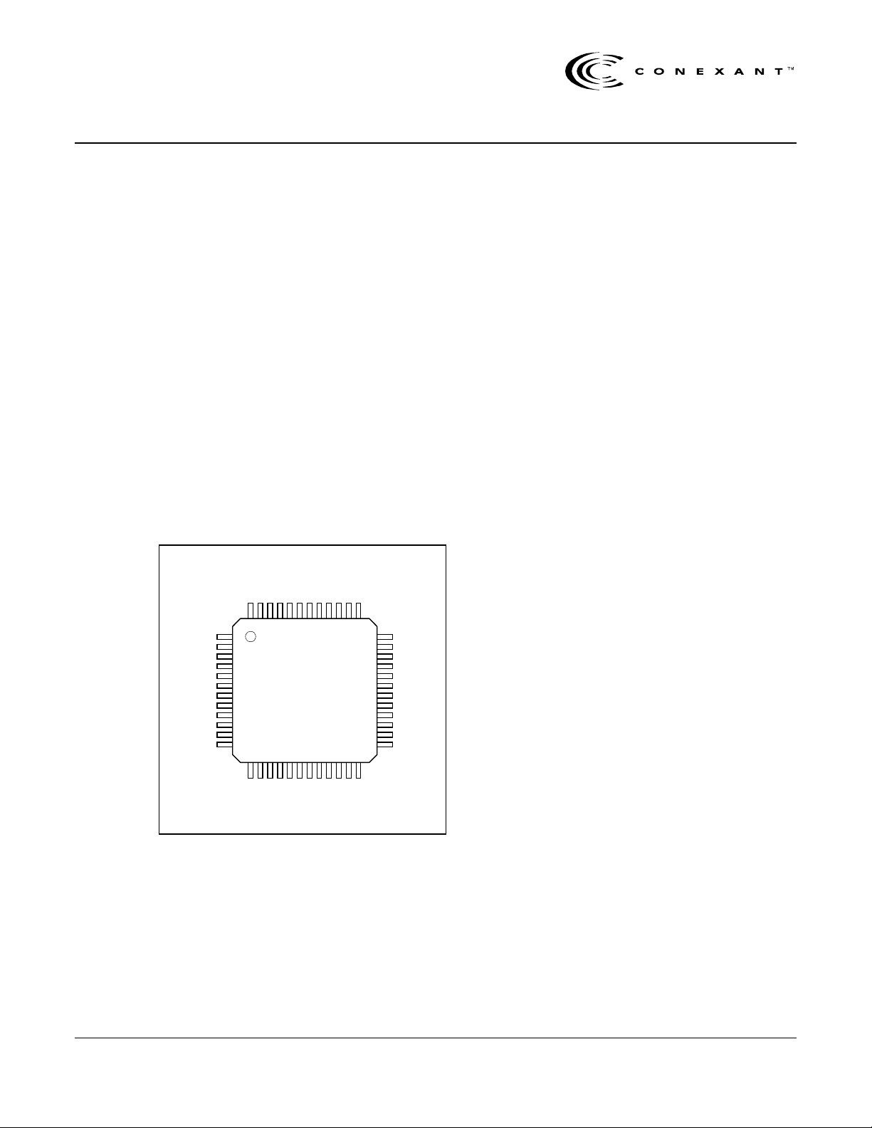
conversion modulator. Figure 1 shows the RF109’s pin signals. Figure 2 shows the
RF109 block diagram.
The RF109 generates the Local Oscillator (LO) frequencies using a Phase Lock Loop
(PLL) frequency synthesizer and an external 2.4 GHz Voltage Controlled Oscillator
(VCO). The PLL provides a full frequency range of 2392.2–2505.6 MHz.
The RF109 features low-voltage operation (3.0–4.5V) for low power consumption. A
complete RF system solution for 2.4 GHz cordless telephone applications can be
constructed with the RF109, a power amplifier, a differential 2.4 GHz frequency source
and a Transmit/Receive (T/R) switch.
VCC6
STROBE
NC8
NC1
CLK
FREF
DATA
TXREF
VCC1
VCC2
TXD
RXEN
LNAATTN
LNAIN
NC2
SYNTHEN
48474645444342
1
2
3
4
5
6
7
8
9
10
11
12
13141516171819
RFO1
GND1
GMCRES
Figure 1. RF109 Pin Signals
VCC5
RF109
RFO2
GND2
NC7
CHPO
TXEN
MIXBPC
NC6
VCO2
NC5
4137403938
2024212223
PS2
PS1
MODSET
VCO1
NC4
36
35
34
33
32
31
30
29
28
27
26
25
AGC
GCREF
NC3
SRI+
SRISRQ+
SRQVCC4
GND3
RXI+
RXIRXQ+
RXQVCC3
Features
• Low power dissipation
• Fast settling from standby mode to active
mode
• Separate enable lines for transmit, receive,
and synthesizer
• 64 programmable channels with 1.8 MHz
channel spacing
• 3-battery-cell operation
• 48-pin TQFP package with exposed paddle
(refer to Figure 6)
Receiver
•
− LNA/Quadrature mixer from RF down to
baseband
− Selectable LNA gain
− Integrated baseband filter with external
bandwidth adjustment
− Receiver baseband amplifier with
automatic gain control
− Direct conversion with differential
baseband outputs
− Low system noise figure (9.0 dB typ ical)
− Large dynamic range (89 dB typical)
Transmitter
•
− Variable gain modulator
− Mixer for baseband-to-RF modulation
− Differential TX inputs and outputs
− Selectable transmitter output levels for
high, medium, and low power modes
Applications
• Digital Spread Spectrum (DSS) cordless
telephone
• Direct sequence spread spectrum systems
• Frequency hopping spread spectrum
systems
• Wireless LANs
• Wireless modems
• Wireless security
• Inventory control systems
Data Sheet Doc. No. 100646A
Conexant Proprietary
January 19, 2000
Page 2
RF109 2400 MHz Digital Spread Spectrum Transceiver
External
CSERVO
LNAIN
LNAATTN
LNA
RXI
GMCRES
AGC
RXQ
o
90
RFO1
RFO2
MODSET
PS1
PS2
Modulator
Gain
Control
Figure 2. RF109 Block Diagram
Technical Description
Receive Path_______________________________________
The LNA provides two gain levels for coarse Automatic Gain
Control (AGC), which are selected via the LNAATTN control.
The signal is down-converted to In-phase and Quadraturephase (I/Q) baseband signals using a matched pair of mixers
and the LO.
The receive baseband bandwidth has a bandpass characteristic.
The I/Q baseband signals are internally low-pass and high-pass
filtered to attenuate out-of-channel signals and to remove DC
components. The low-pass cutoff is determined by the GmC
filters and is set by the R
high-pass cutoff is set by the value of the C
connected between pins 32–33, and pins 34–35.
The baseband high-pass cutoff frequency should be set much
lower than the low-pass cutoff frequency or else the servo loop
will become unstable.
The optimum receive bandwidth values are:
f
= 820 kHz, R
LPF
= 20 kHz, C
f
HPF
gmc
resistor connected to pin 13. The
servo
capacitors
gmc
servo
Ω
= 825
= 0.082 µF
Synthesizer
External
CSERVO
Interface
Serial
Power
Mgmt.
External
VCO
LPF
FREF
STROBE
CLK
DATA
RXEN
SYNTHEN
TXEN
TXD
Transmit Path_______________________________________
The transmit path consists of an amplifier and a mixer. The
mixer modulates the LO with baseband data supplied to pin 8.
The transmit RF outputs from the RF109 are differential and
matched for a 100Ω differential load. If a single-ended
connection is required, then the unused output must be suitably
terminated by a 50Ω resistor (as shown in Figure 5).
The transmit output power is determined by the output power
control inputs, PS1 (pin 21) and PS2 (pin 22), and by the value
mod
of R
(connected to pin 20). R
mod
sets the bias current into the
modulator which is then multiplied by a factor set by the state of
PS1 and PS2. PS1 and PS2 input programming is given in the
Transmitter Section of Table 3.
LO Generation ______________________________________
The LO is generated by a programmable PLL frequency
synthesizer and a 2.4 GHz external VCO. Synthesizer
performance parameters are determined by the loop filter, the
external reference oscillator, the sensitivity and phase noise of
the VCO, and the frequency synthesizer programming.
A matched pair of VGAs provide fine AGC. The differential I/Q
baseband signals are DC-coupled to the RXI+, RXI-, RXQ+, and
RXQ- outputs, respectively.
2
Conexant Proprietary 1/19/00
Conexant
The RF109 requires differential inputs for VCO1 (pin 38) and
VCO2 (pin 39). The typical differential input level is 200 mVp-p.
A BALUN transformer, shown in Figure 5, is used to generate
differential signals from a single-ended VCO output.
100646A
Page 3
2400 MHz Digital Spread Spectrum Transceiver RF109
Synthesizer Programming____________________________
The frequency synthesizer block is comprised of a divide-by-3
counter (D), 9.6 MHz reference frequency (FREF) source, a
fixed reference divider of 16 (R), 16/17 prescaler (M), a fixed
counter of 83 (N), a programmable counter of 64 (A),an external
loop filter, and a 2.4 GHz external VCO.
The synthesizer can be programmed to cover 64 channels
(channel spacing = 1.8 MHz) from 2392.2 MHz to 2505.6 MHz
Table 1).
The LO frequency is given by the following equation:
f
= (D) × (FREF/R) × ((M × N) + (A + 1)),
LO
where N > A.
Example:
= 3 × (9.6 MHz / 16) × ((16 × 83) + 7) = 2403.0 MHz
f
LO
= 3 × (9.6 MHz / 16) × ((16 × 83) + 46) = 2473.2 MHz
f
LO
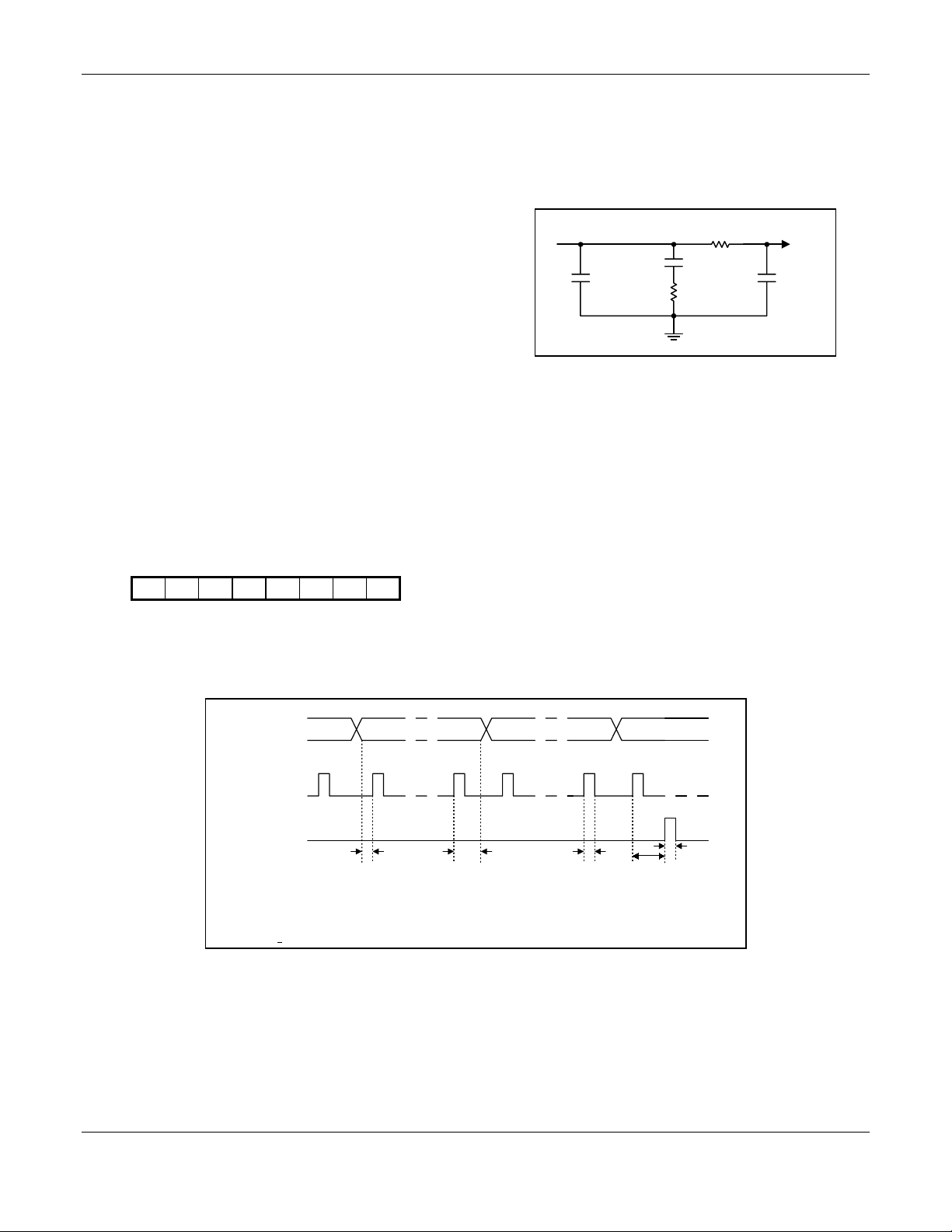
Data Format.
The synthesizer is programmed with a halfduplex 3-wire serial interface. The three signals are DATA, CLK,
and STROBE. Each rising edge of the CLK signal shifts one bit
of the data into a shift register. When the STROBE input is
toggled from low to high, the data latched in the shift register is
transferred to the A counter. The data format is as follows:
Synthesizer Loop Filter.
A typical loop filter design is shown
below in Figure 3. The loop bandwidth is approximately 5 kHz
with a nominal phase margin of 45 degrees for a VCO sensitivity
of 60 MHz/V.
CHPO
pin 43
0.01µF
390
pF
Figure 3. Typical Loop Fi lter
10k
10k
Ω
Ω
VCO
TUNE
330
pF
Power Management__________________________________
Independent power-up/power-down control of the transmit path,
receive path, and frequency synthesizer is provided by the
TXEN, RXEN and SYNTHEN controls, respectively. When all of
the functions are powered down, the current drain from the
voltage supply (Vcc) is at a minimum.
MSB
S7 S6 S5 S4 S3 S2 S1 S0
LSB
The timing relationship is shown in Figure 4. Programming bits
S0 to S5, used for the A counter, are defined in Table 1. Bits S6
and S7 are reserved.
MSB LSB
DATA
CLK
STROBE
t1 t2 t3
t1 =Data setup time
t2 =Data hold time
t3 =Clock pulse-width
t4 =STROBE enable pulse-width
t5 =STROBE setup time to the rising edge of the last clock
>
t1 to t5
1µs each
Figure 4. Timing Diagram
t5
t4
100646A
Conexant
1/19/00 Conexant Proprietary
3
Page 4

RF109 2400 MHz Digital Spread Spectrum Transceiver
Table 1. Swallow C ounter Data Input
Synth. Channel No. (A) Frequency (MHz) S5 S4 S3 S2 S1 S0
0 2392.2 000000
1 2394.0 000001
2 2395.8 000010
.
.
.
6 2403.0 000110
7 2404.8 000111
8 2406.6 001000
.
.
.
25 2437.2 011001
26 2439.0 011010
27 2440.8 011011
.
.
.
45 2473.2 101101
46 2475.0 101110
47 2476.8 101111
.
.
.
61 2502.0 111101
62 2503.8 111110
63 2505.6 111111
.
.
.
.
.
.
.
.
.
.
.
.
.
.
.
.
.
.
.
.
.
.
.
.
.
.
.
.
.
.
.
.
.
.
.
.
.
.
.
.
.
.
.
.
.
.
.
.
.
.
.
.
.
.
.
.
.
.
.
.
.
.
.
.
.
.
.
.
.
.
.
.
.
.
.
.
.
.
.
.
.
.
.
.
4
Conexant
100646A
Conexant Proprietary 1/19/00
Page 5

2400 MHz Digital Spread Spectrum Transceiver RF109
Recommendations on Layout and Implementation _______
A typical applications schematic is shown in Figure 5.
Decouple all Vcc pins as close as possible to the supply pin.
All ground pins should have minimum trace inductance to
ground. If a ground plane cannot be provided right at the pins,
the vias to the ground plane should be placed as close to the
pins as possible. There should be one via for each ground pin. If
the ground plane is at the bottom layer, it is recommended to
have two vias in parallel for each ground pin.
Connect all no connect (NC) pins to the ground.
VCC1 (pin 6), VCC2 (pin 7), VCC3 (pin 25), and VCC4 (pin 31)
should be connected to the common Vcc supply through
individual decoupling networks.
R
should be chosen to provide a typical baseband spread
TXD
spectrum signal level of 0.10 Vp-p, to the TXD pin (pin 8).
The routing of the trace to pin 3 (FREF) is very important to
minimize the coupling of the reference clock (9.6 MHz) into the
VBAT
SYNTHEN
STROBE
CLK
FREF
DATA
VBAT
RXEN
47nF
LNAATTN
47nF
TXD
8.2
pF
8.2pF
8.2pF
8.2pF
8.2pF
8.2pF
10
R
3.6k
Ω
TXD
Ω
Ω
402
3V REGULATOR
CTRL
GND1
BYP
0.056µF
47nF
0.01µF
8.2pF
8.2pF
8.2pF
82µH
820pF
820pF
VCC
GND2
OUT
1500pF
1500pF
402
47
pF
1.0pF
Ω
1.8pF
+
1000
pF
-
VREG
Ω
10
0.01
µF
1
2
3
4
5
6
7
8
9
10
11
12
Rgmc
Ω
825
12pF12pF
8.2
47
pF
µF
Ω
10
8.2
pF
390pF 0.01µF
48474645444342
RF109
13141516171819
Rmod
1.2k
2200
pF
0.047
µF
Ω
LO. The FREF trace should be well isolated from all other
traces, preferably by grounded strips on either side of the trace.
All traces from the VCO to pins 38 and 39 should be as short as
possible with a characteristic impedance of 50 Ω.
Exposed Paddle Soldering____________________________
The RF109 48-pin TQFP package has an exposed (metal)
paddle on the bottom. The footprint dimensions of the exposed
paddle are shown in Figure 6. The printed circuit board should
provide through hole connections to the ground plane to ground
the exposed paddle. The solder mask opening should have the
same size as the exposed paddle. All relevant manufacturing
considerations for this type of package should be taken into
account.
ESD Sensitivity______________________________________
The RF109 is a static-sensitive electronic device. Do not operate
or store near strong electrostatic fields. Take proper
Electrostatic Discharge (ESD) precautions.
8.2
pF
10k
4137403938
2024212223
Ω
Ω
100
36
35
34
33
12pF
12pF
Cservo
0.082µF
Cservo
0.082µF
32
31
30
29
28
27
26
25
0.047
µF
0.047µF
Ω
470
VCO SHIELD AREA
BALUN
OUT
GND
INPUT
OUT
GND
NC
8.2pF
75Ω
Ω
91
VCO
OUT
VCC
Ω
91
GND
GND
NC
TUNE
330pF
Ω
10k
VREG
Ω
10
8.2pF
1000
pF
VBAT
PS1 PS2 AGC RXI+RXI-RXQ+RXQ-LNAIN RFO1 RFO2 TXEN
Figure 5. Typical Application Diagram – RF109
100646A
Conexant
1/19/00 Conexant Proprietary
5
Page 6

RF109 2400 MHz Digital Spread Spectrum Transceiver
Interface Description
Table 2. RF109 Pin Signal Description (1 of 2)
Pin Signal Type Description
1
This differenti al signal pair is the in-phase portion of
This differenti al signal pair is the quadrature
18 TXEN Input
9 RXEN Input
46 SYNTHEN Input
21
22
10 LNAATTN Input
3 FREF Input
2 CLK Input
4 DATA Input
47 STROBE Input
8 TXD Input
5 TXREF Input
23 GCREF Input
28
29
26
27
24 AGC Input
38
39
43 CHPO Output
11 LNAIN Input
15
16
PS1
PS2
RXIRXI+
RXQRXQ+
VCO1
VCO2
RFO1
RFO2
Input
Input
Output
Output
Output
Output
Input
Input
Output
Digital Signals
Transmit Enable.
1: Tx on
0: Tx off
Receive Enable.
1: Rx on
0: Rx off
Synthesizer Enable.
1: Synthesizer on
0: Synthesizer off
Transmit Power.
PS1=0, PS2=0: High (–8 dBm typi cal, single-ended)
PS1=0, PS2=1: Medium (–18 dBm typi cal, single-ended)
PS1=1, PS2=0: Low (–26.5 dBm typical, single-ended)
PS1=1, PS2=1: Undefined
LNA Attenuator.
1: Low gain, attenuator enabled
0: High gain, attenuator disabled
Reference Oscillator.
clock provi des channel spacing of 1. 8 MHz (see Table 1).
Synthesizer Programming Cl ock.
synthesizer input register. The rising edge of CLK is used to load each data bit.
Synthesizer Programming Dat a.
from MSB first t o LSB. The DATA bit is loaded into t he synthesizer i nput register on the ri sing edge of the CLK signal.
Synthesizer Programming St robe.
swallow counter, after all of the data bits have been shifted in. The data is transferred on the rising edge of the STROBE signal.
Transmit Data.
baseband modem. The TXD signal shall be filtered first if any data/s pectral shaping is desired. A resistor divider should be us ed
to provide the desired signal level at t he TXD input of the RF109.
Tx Reference.
Gain Control Reference.
Received In-Phase Signal Negative, Received In-Phase Signal Positive.
the baseband output of the receiver. The differential output signal level is typically 0.5 Vp-p, within the AGC operating range of
1.35–1.9 V.
Received Quadrature Signal Negati ve, Received Quadrature Signal Posit ive.
portion of the baseband output of the receiver. The differential output signal level is typically 0.5 Vp-p, within the AGC operating
range of 1.35–1.9 V.
Auto Gain Control.
generated by the baseband ASIC as part of the AGC control loop. An increase in the AGC voltage decreases the baseband VGA
gain. The control loop pr ovides a typical receive baseband diff erential signal of 0. 5 Vp-p over the VAGC range of 1.35–1.9 V.
Voltage Controlled Oscillator.
mixers. An external BALUN may be used to conver t a single-ended external VCO signal to the differ ential signals, VCO1 and
VCO2, required by the RF109. The di fferential input s ignal level required i s typically 200 mVp-p.
Charge Pump Output.
RF Input.
50 Ω. The received signal must be AC coupled into LNAIN wi th a 12 pF series capaci tor.
RF Output.
RF output signals are internally AC-coupl ed. The unused signal should be t erminated to ground through a 50 Ω resistor.
Switches on/off bias power to the transmi tter circuitry.
Switches on/off bias power to the receiver circuitry.
Switches on/off bias power to the synthesizer circuitry.
These two control bits select the PA output power.
This control signal toggles the LNA gain between t he low gain state and the high gain state.
This digital input clock signal i s used to provide the r eference frequency f or the synthesizer. A 9.6 MHz
This is the clock input signal us ed to serially s hift the synthes izer data bits into the
This is the serial data input bit st ream used to program the sy nthesizer. Data bits are shifted
This signal is used to transfer the synthesizer data bits from the input register to the pulse
Analog Signals
This input signal i s used as the modulating s ignal. TXD is a single-ended, 1.2 Mbps NRZ signal fr om the
This is the reference for the TXD input. I t is AC-coupled to ground.
This is the reference for the gain control input. It is connected to ground.
This analog input signal is used to control the gain of the baseband VGAs in the receiver. This signal is
This differential input provides the local oscillator signal from an external VCO to the RF109
This output signal i s used to control the external 2.4 GHz VCO. The CHPO current is typically ±250 µA.
This is the received RF input signal that is routed to the LNA of t he RF109. This pin should be ext ernally matched to
These are the differential transmit output signals from the RF109. The single-ended output impedance is 50 Ω. The
6
Conexant
100646A
Conexant Proprietary 1/19/00
Page 7

2400 MHz Digital Spread Spectrum Transceiver RF109
Table 2. RF109 Pin Signal Description (2 of 2)
Pin Signal Type Description
Miscellaneous
20 MODSET —
13 GMCRES — GMC resistor to set the cutoff fr equency of the baseband filter.
19 MIXBPC — Mixer bias bypass capacitor.
32
33
34
35
1, 12, 36, 37,
40, 41, 42,
48
6 VCC1 Supply Positive supply terminal.
7 VCC2 Supply Positive supply terminal.
25 VCC3 Supply Positive supply terminal.
31 VCC4 Supply Positive supply terminal.
44 VCC5 Supply Positive supply terminal.
45 VCC6 Supply Positive supply terminal.
14, 17, 30 GND Supply Power supply ground terminal.
Notes:
1. All digital si gnals are CMOS compatible.
SRQSRQ+
SRISRI+
NC —
Modulator Gain Setting.
— Q channel DC offset cancel lation servo capac itor connections .
— I channel DC offset canc ellation servo capacitor connections.
No Connect.
It is recommended to connect these pins t o ground.
Transmit modulator gai n can be adjusted by the res istor connected t o the pin.
Power Supply Terminals
100646A
Conexant
1/19/00 Conexant Proprietary
7
Page 8

RF109 2400 MHz Digital Spread Spectrum Transceiver
Specifications
Table 3. Electrical Specifications
Note: TA = 25oC, VCC = 3.6 V, fLO= 2449.8 MHz
(1)
(1 of 3)
Parameter Min Typical Max Units
Receiver Section
RX voltage gain: LNA high-gain mode (LNAATTN = 0)
LNA gain step delta Gain LNAATTN = 0/1 27 dB
RX gain variation vs. frequency 2400 MHz < fLO < 2483.5 MHz
RX SSB noise figure: High-gain mode, GC = 1.35 V 9 dB
RX input IP3: LNA high-gain mode, GC = 1.9 V
RX input P1dB: LNA high-gain mode (LNAATTN = 0)
LNA low-gain mode (LNAATTN = 1)
I/Q phase imbalance ±7 deg
I/Q amplitude imbalance 3dB
Input high voltage, LNAATTN, RXEN VIH 1.9 V
Input low voltage, LNAATTN, RXEN VIL 0.75
Input high current, RXEN IIH 125 200
Input low current , RXEN IIL –10 10
Input high current, LNAATTN IIH 60
Input low current, LNAATTN IIL –10
GC Iin –500 500
Baseband amplifier gain c ontrol range (GC = 1.35–1.9 V) 63 dB
GC input voltage range 1.35 1.65 1.9 V
Baseband amplifier gain c ontrol sensitivity GC = 1.35–1.9 V
RX P1dB @ 3.9 MHz offset LNA high gain, GC=1.9V –24 dBm
Baseband output load capacitance 20 50 pF
Baseband LPF 3 dB bandwidth (Rgmc = 825 Ω)
Baseband selectivity @ 3.9 MHz 60 70 dB
Baseband common mode output 1.0 Vcc – 1.55 Vcc – 1.0 V
Baseband I,Q DC offset 25 mV
RXI, RXQ DC and gain settle ti me
at TDD rate > 250 Hz
Baseband HPF 3dB bandwidth (servo capacitors = 82 nF) 13 22 29 kHz
Baseband output voltage swing (peak differential) 250 mVp
Baseband output SNR (GC = 1.9 V) 31 dB
GC = 1.35 V
GC = 1.65 V
GC = 1.9 V
LNA low-gain mode, GC = 1.9 V
GC = 1.35 V
GC = 1.65 V
GC = 1.9 V
GC = 1.9 V
GC = 1.35 V
GC = 1.65 V
GC = 1.90 V
(2)
from initial RXEN input
94.5 100
76
37
–1.5 0.5 2.0 dB
–33
–3
–90.5
–65
–36
–10
0.14
0.01
0.15
0.13
650 820 970 kHz
50 100
105.5 dB
dBm
dBm
0.17 dB/mV
µ
A
µ
A
µ
A
µ
s
8
Conexant
100646A
Conexant Proprietary 1/19/00
Page 9

2400 MHz Digital Spread Spectrum Transceiver RF109
Table 3. Electrical Specifications (2 of 3)
Parameter Min Typical Max Units
Transmitter Section
Gain variation vs. frequency 2400 MHz < fLO < 2483.5 MHz
Peak-envelope output power (single-ended):
High power mode (PS1 = 0, PS2 = 0)
Medium power mode (PS1 = 0, PS2 = 1)
Low power mode (PS1 = 1, PS2 = 0)
Undefined mode (PS1 = 1, PS2 = 1)
IM3 (TXD input signal 2 tones each 60 mVpp) –35 dBc
LO suppression relative to peak –25 –15 dBc
TXD input impedance 10
TXD input peak-to-peak baseband spread spectrum signal for specified output
peak envelope power
TXD input bandwidth 80 MHz
TXD to RF settle time to within spec value from TXEN 50
Input high voltage, PS1, PS2, TXEN VIH
Input low voltage, PS1, PS2, TXEN VIL
Input high current, PS1, PS2, TXEN IIH
Input low current, PS1, PS2, TXEN IIL –10
Input high current TXEN IIH
Input low current TXEN IIL –10
Synthesizer frequency range 2392.2 2505.6 MHz
Differential LO input power across VCO1 and VCO2 –17 –13 –9 dBm
Input reference fr equency, FREF 9.6 MHz
Frequency step, F
Comparison frequency (600 kHz) spur level –60 dBc
Input high voltage, STROBE, CLK, DATA, SYNTHEN VIH
Input low voltage, STROBE, CLK, DATA, SYNTHEN VIL
Input high current, STROBE, CLK, DATA IIH
Input low current, STROBE, CLK, DATA IIL –10
Input high current, SYNTHEN IIH
Input low current, SYNTHEN IIL –10
Input high voltage, FREF VIH
Input low voltage, FREF VIL
Input high current, FREF IIH
Input low current, FREF IIL –10
Charge-pump output current
Output short-ci rcuit current CHPO 1.0 mA
S
(3)
–10.5 –8.0
1.9
Frequency Synthesizer Section
1.9
1.9
0.5 1.5 dB
–18
–26.5
not used
100 mV
1800 kHz
±
250
–5.0 dBm
0.75
60
100
0.75
40 µA
100 µA
0.75
100 µA
k
µ
µ
µ
µA
Ω
pp
s
V
A
A
V
V
100646A
Conexant
1/19/00 Conexant Proprietary
9
Page 10

RF109 2400 MHz Digital Spread Spectrum Transceiver
Table 3. Electrical Specifications (3 of 3)
Parameter Min Typical Max Units
Power Supply
Total supply current:
RX mode (RXEN, SYNTHEN = 1)
TX + SYNTH supply current :
Synth mode (SYNTHEN = 1)
Sleep mode (RXEN, TXEN, SYNTHEN, LNAATTN = 0)
Power supply range
Notes:
1. The specifications in Table 3 are guaranteed at a supply voltage of 3.6 VDC, and T
2. Gain settled to within 90% of final value, DC set tled to within 10% of desir ed signal’s final value.
3. TXD input signal 120 mVpp, 300 kHz sinusoidal at pin 8, Rmod = 1.2 kΩ.
(1)
(3)
High power mode
Medium power mode
Low power mode
67
31
3.0 3.6 4.5 VDC
A
= 25oC.
89
41
33
31
25
5
111
51
100
mA
mA
mA
mA
mA
µA
Table 4. Absolute Maximum Ratings
Parameter Min Max Unit
Supply voltage (Vcc)
Input voltage range
Power dissipation 700 mW
LNA input power +5 dBm
Operating temperature range (TA) –10 70
Storage temperature –40 125 °C
Notes:
1. Voltages are referenced to GND.
1
1
–0.3 5 V
–0.3 VCC V
°
C
10
Conexant
100646A
Conexant Proprietary 1/19/00
Page 11

2400 MHz Digital Spread Spectrum Transceiver RF109
Device Dimensions
RF109 device dimensions are shown below in Figure 6.
D
D1
D2
Exposed
paddle
(bottom side)
D2D1D
Exposed
paddle
e b
A2
A
A1
DETAIL A
D3
DETAIL A
c
L
L1
* Metric values (millimeters) should be used for
PCB layout. English values (inches) are
converted from metric values and may contain
round-off errors.
Figure 6. RF109 Device Dimensions
D1
Dim.
A
A1
A2
D
D1
D2
D3
L
L1
e
b
c
Coplanarity
Ref. 48-PIN TQFP (GP00-D495-003)
Millimeters Inches*
Min. Max. Min. Max.
1.6 MAX
0.05 0.10
1.35 1.45
8.85 9.15
6.95 7.05
5.5 REF
3.198
0.5 0.75
1.0 REF
0.500 REF
0.220 REF
0.11 0.17
0.10 MAX 0.0039 MAX
0.0630 MAX
0.0020 0.0039
0.0528 0.0571
0.3484 0.3602
0.2736 0.2776
0.2165 REF
0.0197 0.0295
0.0394 REF
0.0197 REF
0.0087 REF
0.0043 0.0067
0.1259
Copyright © 2000, Conexant Systems, Inc . All Rights Reserved.
Information in thi s document is provi ded in connection with Conexant Systems, Inc . (“Conexant”) products. These materi als are provided by Conex ant as a service t o its
customers and may be used for informational purposes only. Conexant assumes no responsibility for errors or omissions in these mat erials. Conexant may make changes to
specifications and product descr iptions at any time, without notice. Conex ant makes no commitment t o update the information contained herein. Conexant shall have no
responsibility whatsoever f or conflicts or incompatibilities arising from future changes to it s specifications and product descriptions.
No license, express or implied, by estoppel or otherwise, to any intellectual property rights is granted by this document. Exc ept as provided in Conexant’s Terms and
Conditions of Sale for such pr oducts, Conexant assumes no liability whatsoever.
THESE MATERIALS ARE PROVIDED “AS IS” WITHOUT WARRANTY OF ANY KIND, EI THER EXPRESS OR IMPLIED, RELATING TO SALE AND/OR USE OF
CONEXANT PRODUCTS INCLUDING LIABILITY OR WARRANTIES RELATING TO FITNESS FOR A PARTI CULAR PURPOSE, MERCHANTABILITY, OR
INFRINGEMENT OF ANY PATENT, COPYRIGHT OR OTHER INTELLECTUAL PROPERTY RIGHT. Conex ant further does not warr ant the accuracy or completeness of
the information, t ext, graphics or other items contained within these material s. Conexant shall not be liable for any special, indirect, incidental, or consequential damages,
including without limitation, lost revenues or lost profits, which may result from the use of these materials.
Conexant products ar e not intended for use in medical, life savi ng or life sustaining applications. Conexant customers using or selling Conexant products for use i n such
applications do so at their own risk and agree to fully indemnify Conexant for any damages resulting from such improper use or sale.
The following are trademarks of Conexant Systems, Inc.: Conexant, the Conexant C symbol , and “What’s Next i n Communications Technologies”. Product names or
services l isted in this publi cation are for identification purposes only, and may be trademarks of third parties. Third-party brands and names are the property of their
respective owners.
100646A
Conexant
1/19/00 Conexant Proprietary
11
Page 12

Further Information:
literature@conexant.com
1-800-854-8099 (North America)
33-14-906-3980 (International)
Web Site
www.conexant.com
Hong Kong
Phone: (852) 2 827 0181
Fax: (852) 2 827 6488
India
Phone: (91 11) 692 4780
Fax: (91 11) 692 4712
World Headquarters
Conexant Systems, Inc.
4311 Jamboree Road,
P.O. Box C
Newport Beach, CA 92658-8902
Phone: (949) 483-4600
Fax: (949) 483-6375
U.S. Florida/So uth America
Phone: (727) 799-8406
Fax: (727) 799-8306
U.S. Los Angeles
Phone: (805) 376-0559
Fax: (805) 376-8180
U.S. Mid-Atlantic
Phone: (215) 244-6784
Fax: (215) 244-9292
U.S. North Central
Phone: (630) 773-3454
Fax: (630) 773-3907
U.S. Northeast
Phone: (978) 692-7660
Fax: (978) 692-8185
U.S. Northwest/Pacific West
Phone: (408) 249-9696
Fax: (408) 249-7113
U.S. South Central
Phone: (972) 733-0723
Fax: (972) 407-0639
U.S. Southeast
Phone: (919) 858-9110
Fax: (919) 858-8669
U.S. Southwest
Phone: (949) 483-9119
Fax: (949) 483-9090
APAC Headquarters
Conexant Systems Singapore,
Pte. Ltd.
1 Kim Seng Promenade
Great World City
#09-01 East Tower
Singapore 237994
Phone: (65) 737 7355
Fax: (65) 737 9077
Australia
Phone: (61 2) 9869 4088
Fax: (61 2) 9869 4077
China
Phone: (86 2) 6361 2515
Fax: (86 2) 6361 2516
Korea - Seoul Office
Phone: (82 2) 565 2880
Fax: (82 2) 565 1440
Korea - Taegu Office
Phone: (82 53) 745 2880
Fax: (82 53) 745 1440
Europe Headquarters
Conexant Systems France
Les Taissounieres B1
1681 Route des Dolines
BP 283
06905 Sophia Antipolis Cedex
France
Phone: (33 1) 41 44 36 50
Fax: (33 1) 93 00 33 03
Europe Central
Phone: (49 89) 829 1320
Fax: (49 89) 834 2734
Europe Mediterranean
Phone: (39 02) 9317 9911
Fax (39 02) 9317 9913
Europe North
Phone: (44 1344) 486 444
Fax: (44 1344) 486 555
Europe South
Phone: (33 1) 41 44 36 50
Fax: (33 1) 41 44 36 90
Middle East Headquarte rs
Conexant Systems Commercial
(Israel) Ltd.
P.O. Box 12660
Herzlia 46733
Israel
Phone: (972 9) 952 4064
Fax: (972 9) 951 3924
Japan Headquarters
Conexant Systems Japan Co., Ltd.
Shimomoto Bui lding
1-46-3 Hatsudai,
Shibuya-ku
Tokyo, 151-0061
Japan
Phone: (81 3) 5371 1567
Fax: (81 3) 5371 1501
Taiwan Headquar ters
Conexant Systems, Taiwan Co., Ltd.
Room 2808
International Trade Building
333 Keelung Road, Section 1
Taipei 110
Taiwan, ROC
Phone: (886 2) 2720 0282
Fax: (886 2) 2757 6760
 Loading...