

Page 1
®
RCV420
Precision 4mA to 20mA
CURRENT LOOP RECEIVER
RCV420
FEATURES
● COMPLETE 4-20mA TO 0-5V CONVERSION
● INTERNAL SENSE RESISTORS
● PRECISION 10V REFERENCE
● BUILT-IN LEVEL-SHIFTING
±40V COMMON-MODE INPUT RANGE
●
● 0.1% OVERALL CONVERSION ACCURACY
● HIGH NOISE IMMUNITY: 86dB CMR
DESCRIPTION
The RCV420 is a precision current-loop receiver designed to convert a 4–20mA input signal into a 0–5V
output signal. As a monolithic circuit, it offers high
reliability at low cost. The circuit consists of a premium grade operational amplifier, an on-chip precision
resistor network, and a precision 10V reference. The
RCV420 features 0.1% overall conversion accuracy,
86dB CMR, and ±40V common-mode input range.
The circuit introduces only a 1.5V drop at full scale,
which is useful in loops containing extra instrument
burdens or in intrinsically safe applications where
APPLICATIONS
● PROCESS CONTROL
● INDUSTRIAL CONTROL
● FACTORY AUTOMATION
● DATA ACQUISITION
● SCADA
● RTUs
● ESD
● MACHINE MONITORING
transmitter compliance voltage is at a premium. The
10V reference provides a precise 10V output with a
typical drift of 5ppm/°C.
The RCV420 is completely self-contained and offers a
highly versatile function. No adjustments are needed
for gain, offset, or CMR. This provides three important
advantages over discrete, board-level designs: 1) lower
initial design cost, 2) lower manufacturing cost, and
3) easy, cost-effective field repair of a precision circuit.
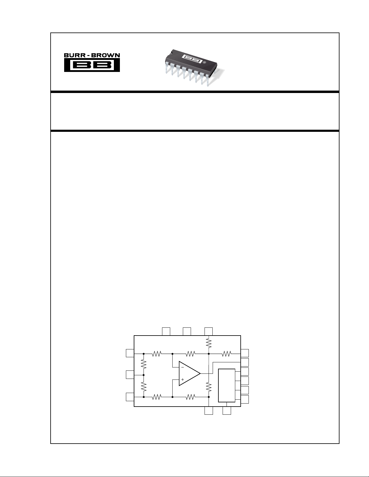
V+ V– Ref In
16 4 12
RCV420
1
–In
2
C
T
+In
3
International Airport Industrial Park • Mailing Address: PO Box 11400, Tucson, AZ 85734 • Street Address: 6730 S. Tucson Blvd., Tucson, AZ 85706 • Tel: (520) 746-1111 • Twx: 910-952-1111
Internet: http://www.burr-brown.com/ • FAXLine: (800) 548-6133 (US/Canada Only) • Cable: BBRCORP • Telex: 066-6491 • FAX: (520) 889-1510 • Immediate Product Info: (800) 548-6132
©
1988 Burr-Brown Corporation PDS-837E Printed in U.S.A. October, 1997
300kΩ
RS
75Ω
R
75Ω
300kΩ
S
99kΩ
1.01kΩ
100kΩ
1
92kΩ
13 5
Rcv
Com
11.5kΩ
+10V
Ref
Ref
Com
15
14
11
10
Rcv f
B
Rcv Out
Ref Out
Ref f
B
Ref Trim
8
Ref Noise Reduction
7
®
RCV420
Page 2
SPECIFICATIONS
ELECTRICAL
At T = +25°C and VS = ±15V, unless otherwise noted.
RCV420KP, JP
CHARACTERISTICS MIN TYP MAX UNITS
GAIN
Initial 0.3125 V/mA
Error 0.05 0.15 % of span
Error—JP Grade 0.25 % of span
vs Temp 15 ppm/°C
Nonlinearity
OUTPUT
Rated Voltage (I
Rated Current (E
Impedance (Differential) 0.01 Ω
Current Limit (To Common) +49, –13 mA
Capacitive Load 1000 pF
INPUT
Sense Resistance 74.25 75 75.75 Ω
Input Impedance (Common-Mode) 200 kΩ
Common-Mode Voltage ±40 V
CMR
AC 60Hz 80 dB
OFFSET VOLTAGE (RTO)
Initial 1mV
ZERO ERROR
Initial 0.025 0.075 % of span
Initial—JP Grade 0.15 % of span
OUTPUT NOISE VOLTAGE
f
B
f
O
DYNAMIC RESPONSE
Gain Bandwidth 150 kHz
Full Power Bandwidth 30 kHz
Slew Rate 1.5 V/µs
Settling Time (0.01%) 10 µs
VOLTAGE REFERENCE
Initial 9.99 10.01 V
Trim Range
Noise (0.1Hz to 10Hz) 5 µVp-p
Output Current +10, –2 mA
POWER SUPPLY
Rated ±15 V
Voltage Range
Quiescent Current (V
TEMPERATURE RANGE
Specification 0 +70 °C
Operation –25 +85 °C
Storage –40 +85 °C
Thermal Resistance,
NOTES: (1) Nonlinearity is the max peak deviation from best fit straight line. (2) With 0 source impedance on Rcv Com pin. (3) Referred to output with all inputs
grounded including Ref In. (4) With 4mA input signal and Voltage Reference connected (includes V
slightly affects drift. (6) I
(1)
= +10mA, –5mA) 10 12 V
O
= 10V) +10, –5 mA
O
0.0002 0.002 % of span
(Stable Operation)
(2)
vs Temp (DC) (T
A
= T
MIN
to T
)76dB
MAX
(3)
70 80 dB
vs Temp 10 µV/°C
vs Supply (±11.4V to ±18V) 74 90 dB
vs Time 200 µV/mo
(4)
vs Temp 10 ppm of
span/°C
= 0.1Hz to 10Hz 50 µVp-p
= 10kHz 800 nV/√Hz
(5)
±4%
vs Temp 5 ppm/°C
vs Supply (±11.4V to ±18V) 0.0002 %/V
vs Output Current (I
vs Time 15 ppm/kHz
= 0 to +10mA) 0.0002 %/mA
O
(6)
= 0V) 3 4 mA
O
θ
JA
Ref = 5mA, IO Rcv = 2mA.
O
–5, +11.4 ±18 V
80 °C/W
, Gain Error, and Voltage Reference Errors). (5) External trim
OS
®
RCV420
2
Page 3
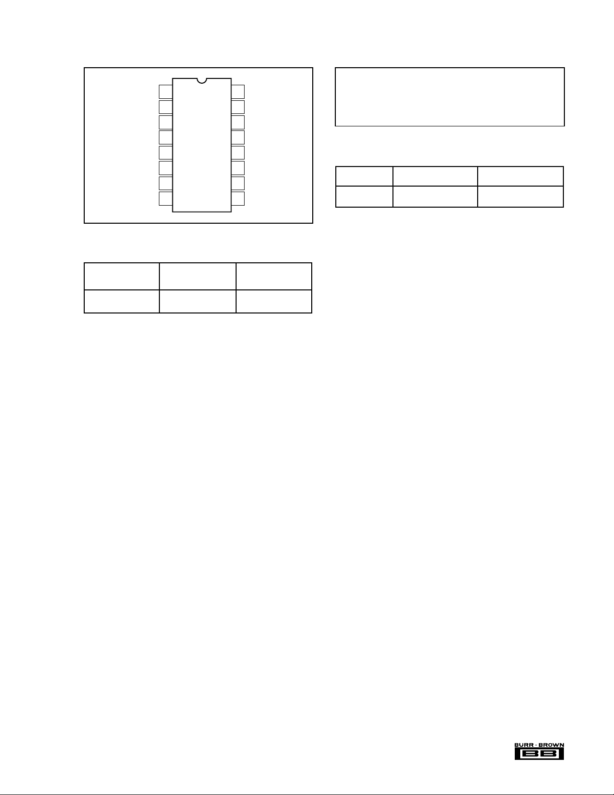
PIN CONFIGURATION
Top View DIP
–In
C
+In
V–
Ref Com
NC
Ref Noise Reduction
Ref Trim
1
2
T
3
4
5
6
7
8
16
15
14
13
12
11
10
9
V+
Rcv f
B
Rcv Out
Rcv Com
Ref In
Ref Out
Ref f
B
NC
ORDERING INFORMATION
ABSOLUTE MAXIMUM RATINGS
Supply ...............................................................................................±22V
Input Current, Continuous ................................................................ 40mA
Input Current Momentary, 0.1s ........................... 250mA, 1% Duty Cycle
Common-Mode Input Voltage, Continuous ....................................... ±40V
Lead Temperature (soldering, 10s)............................................... +300°C
Output Short Circuit to Common (Rcv and Ref) ..................... Continuous
NOTE: (1) Stresses above these ratings may cause permanent damage.
(1)
PACKAGE INFORMATION
PRODUCT PACKAGE NUMBER
RCV420KP 16-Pin Plastic DIP 180
RCV420JP 16-Pin Plastic DIP 180
NOTE: (1) For detailed drawing and dimension table, please see end of data
sheet, or Appendix C of Burr-Brown IC Data Book.
PACKAGE DRAWING
(1)
PRODUCT GRADE PACKAGE
RCV420KP 0°C to +70°C 16-Pin Plastic DIP
RCV420JP 0°C to +70°C 16-Pin Plastic DIP
PERFORMANCE
The information provided herein is believed to be reliable; however, BURR-BROWN assumes no responsibility for inaccuracies or omissions. BURR-BROWN assumes
no responsibility for the use of this information, and all use of such information shall be entirely at the user’s own risk. Prices and specifications are subject to change
without notice. No patent rights or licenses to any of the circuits described herein are implied or granted to any third party. BURR-BROWN does not authorize or warrant
any BURR-BROWN product for use in life support devices and/or systems.
3
RCV420
®
Page 4

TYPICAL PERFORMANCE CURVES
At TA = +25°C, VS = ±15V, unless otherwise noted.
STEP RESPONSE
NO LOAD
POSITIVE COMMON-MODE VOLTAGE RANGE
80
70
60
50
40
Positive Common-Mode Range (V)
30
vs POSITIVE POWER SUPPLY VOLTAGE
TA = +25°C
11
12 13 14 15 16 17 18 19 20
11.4
Positive Power Supply Voltage (V)
TA = –55°C
TA = +125°C
Max Rating = 40V
–VS = –5V to –20V
SMALL SIGNAL RESPONSE
NO LOAD
Negative Common-Mode Range (V)
SMALL SIGNAL RESPONSE
R
= ∞, CL = 1000pF
L
NEGATIVE COMMON-MODE VOLTAGE RANGE
–80
–70
–60
–50
–40
–30
–20
–10
vs NEGATIVE POWER SUPPLY VOLTAGE
TA = +25°C
Max Rating = –40V
–5 –20
–10 –15
Negative Power Supply Voltage (V)
TA = –55°C to +125°C
+VS = +11.4V to +20V
COMMON-MODE REJECTION
100
80
CMR (dB)
60
40
1 10 100 1k 10k 100k
®
vs FREQUENCY
Frequency (Hz)
RCV420
POWER-SUPPLY REJECTION
100
90
80
PSR (dB)
60
40
1 10 100 1k 10k 100k
vs FREQUENCY
V+ V–
Frequency (Hz)
4
Page 5

THEORY OF OPERATION
Refer to the figure on the first page. For 0 to 5V output with
4–20mA input, the required transimpedance of the circuit is:
V
To achieve the desired output (0V for 4mA and 5V for
20mA), the output of the amplifier must be offset by an
amount:
V
The input current signal is connected to either +In or –In,
depending on the polarity of the signal, and returned to
ground through the center tap, C
matched 75Ω sense resistors, R
tion of common-mode voltage signals on C
ential current-to-voltage conversion. The sense resistors
convert the input current signal into a proportional voltage,
which is amplified by the differential amplifier. The voltage
gain of the amplifier is:
A
The tee network in the feedback path of the amplifier
provides a summing junction used to generate the required
–1.25V offset voltage. The input resistor network provides
high-input impedance and attenuates common-mode input
voltages to levels suitable for the operational amplifier’s
common-mode signal capabilities.
= 5V/16mA = 0.3125V/mA.
OUT/IIN
= –(4mA)(0.3125V/mA) = –1.25V.
OS
. The balanced input—two
T
—provides maximum rejec-
S
T
= 5V/(16mA)(75Ω) = 4.1667V/V.
D
and true differ-
necessary level shifting. If the Ref In pin is not used for level
shifting, then it must be grounded to maintain high CMR.
GAIN AND OFFSET ADJUSTMENT
Figure 2 shows the circuit for adjusting the RCV420 gain.
Increasing the gain of the RCV420 is accomplished by
inserting a small resistor in the feedback path of the amplifier. Increasing the gain using this technique results in CMR
degradation, and therefore, gain adjustments should be kept
as small as possible. For example, a 1% increase in gain is
typically realized with a 125Ω resistor, which degrades
CMR by about 6dB.
A decrease in gain can be achieved by placing matched
resistors in parallel with the sense resistors, also shown in
Figure 2. The adjusted gain is given by the following
expression
V
= 0.3125 x RX/(RX + RS).
OUT/IIN
A 1% decrease in gain can be achieved with a 7.5kΩ
resistor. It is important to match the parallel resistance on
each sense resistor to maintain high CMR. The TCR mismatch between the two external resistors will effect gain
error drift and CMR drift.
There are two methods for nulling the RCV420 output offset
voltage. The first method applies to applications using the
internal 10V reference for level shifting. For these applica-
BASIC POWER SUPPLY
AND SIGNAL CONNECTIONS
Figure 1 shows the proper connections for power supply and
signal. Both supplies should be decoupled with 1µF tantalum capacitors as close to the amplifier as possible. To avoid
gain and CMR errors introduced by the external circuit,
connect grounds as indicated, being sure to minimize ground
resistance. The input signal should be connected to either
+In or –In, depending on its polarity, and returned to ground
through the center tap, C
. The output of the voltage refer-
T
ence, Ref Out, should be connected to Ref In for the
I
IN
4–20mA
+In 3
C
T
–In 1
2
R
75Ω
S
V+
RCV420
16
1µF1µF
4
V–
75Ω
R
S
–In
C
+In
T
10kΩ
10kΩ
(1)
(1)
1
R
X
2
R
X
3
15
RCV420
NOTE: (1) Typical values. See text.
FIGURE 2. Optional Gain Adjustment.
12 Ref In
13
Rcv Com
+10V
Reference
5
Ref Com
15 Rcv f
14 Rcv Out
11 Ref Out
10 Ref f
8 Ref Trim
7 Ref Noise Reduction
B
B
200Ω
(1)
14
V
(0–5V)
O
R
1
±0.5% Gain
Adjustment
Rcv Out
FIGURE 1. Basic Power Supply and Signal Connections.
®
5
RCV420
Page 6

tions, the voltage reference output trim procedure can be
used to null offset errors at the output of the RCV420. The
voltage reference trim circuit is discussed under “Voltage
Reference.”
When the voltage reference is not used for level shifting or
when large offset adjustments are required, the circuit in
Figure 3 can be used for offset adjustment. A low impedance
on the Rcv Com pin is required to maintain high CMR.
ZERO ADJUSTMENT
Level shifting the RCV420 output voltage can be achieved
using either the Ref In pin or the Rcv Com pin. The
disadvantage of using the Ref In pin is that there is an 8:1
voltage attenuation from this pin to the output of the RCV420.
Thus, use the Rcv Com pin for large offsets, because the
voltage on this pin is seen directly at the output. Figure 4
shows the circuit used to level-shift the output of the RCV420
–In
1
C
T
2
RCV420
+In
3
12
±150mV adjustment at output.
15
14
5
13
OPA237
V
O
100kΩ
1kΩ
+15V
100kΩ
–15V
FIGURE 3. Optional Output Offset Nulling Using External
Amplifier.
using the Rcv Com pin. It is important to use a low-output
impedance amplifier to maintain high CMR. With this method
of zero adjustment, the Ref In pin must be connected to the
Rcv Com pin.
MAINTAINING COMMON-MODE REJECTION
Two factors are important in maintaining high CMR: (1)
resistor matching and tracking (the internal resistor network
does this) and (2) source impedance. CMR depends on the
accurate matching of several resistor ratios. The high accuracies needed to maintain the specified CMR and CMR
temperature coefficient are difficult and expensive to reliably achieve with discrete components. Any resistance imbalance introduced by external circuitry directly affects
CMR. These imbalances can occur by: mismatching sense
resistors when gain is decreased, adding resistance in the
feedback path when gain is increased, and adding series
resistance on the Rcv Com pin.
The two sense resistors are laser-trimmed to typically match
within 0.01%; therefore, when adding parallel resistance to
decrease gain, take care to match the parallel resistance on
each sense resistor. To maintain high CMR when increasing
the gain of the RCV420, keep the series resistance added to
the feedback network as small as possible. Whether the Rcv
Com pin is grounded or connected to a voltage reference for
level shifting, keep the series resistance on this pin as low as
possible. For example, a resistance of 20Ω on this pin
degrades CMR from 86dB to approximately 80dB. For
applications requiring better than 86dB CMR, the circuit
shown in Figure 5 can be used to adjust CMR.
PROTECTING THE SENSE RESISTOR
The 75Ω sense resistors are designed for a maximum continuous current of 40mA, but can withstand as much as
250mA for up to 0.1s (see absolute maximum ratings).
There are several ways to protect the sense resistor from
Use 10V Ref for +
–In
1
C
T
2
+In
3
12
V
ZERO
±5V adjustment
at output.
RCV420
10
5
13
OPA237
and 10V Ref with INA105 for –.
15
14
11
10kΩ
10kΩ
+10V
V
= (0.3125)(IIN) + V
O
V
O
2
3
50kΩ
INA105
Procedure:
ZERO
5
–10V
6
1
RCV420
13
1k
1kΩ
1. Connect CMV to C
2. Adjust potentiometer for near zero
at the output.
Ω
1kΩ
OPA237
1kΩ
200Ω
CMR
Adjust
.
T
FIGURE 4. Optional Zero Adjust Circuit. FIGURE 5. Optional Circuit for Externally Trimming CMR.
®
RCV420
6
Page 7

overcurrent conditions exceeding these specifications. Refer
to Figure 6. The simplest and least expensive method is a
resistor as shown in Figure 6a. The value of the resistor is
determined from the expression
R
= VCC/40mA – 75Ω
X
and the full scale voltage drop is
= 20mA x RX.
V
RX
For a system operating off of a 32V supply R
V
= 14.5V. In applications that cannot tolerate such a
RX
= 725Ω and
X
large voltage drop, use circuits 6b or 6c. In circuit 6b a
power JFET and source resistor are used as a current limit.
The 200Ω potentiometer, R
, is adjusted to provide a current
X
limit of approximately 30mA. This circuit introduces a
1– 4V drop at full scale. If only a very small series voltage
drop at full scale can be tolerated, then a 0.032A series 217
fast-acting fuse should be used, as shown in Figure 6c.
For automatic fold-back protection, use the circuit shown in
Figure 15.
V+
V
R
RX
X
4–20mA
V+
R
X
2N3970
200Ω
2
1
= (V+)/40mA – 75Ω
a) R
X
4–20mA
2
1
3
3
RCV420
RCV420
15
V
14
15
14
O
V
O
VOLTAGE REFERENCE
The RCV420 contains a precision 10V reference. Figure 8
shows the circuit for output voltage adjustment. Trimming
the output will change the voltage drift by approximately
0.007ppm/°C per mV of trimmed voltage. Any mismatch in
TCR between the two sides of the potentiometer will also
affect drift, but the effect is divided by approximately 5. The
trim range of the voltage reference using this method is
typically ±400mV. The voltage reference trim can be used to
trim offset errors at the output of the RCV420. There is an
8:1 voltage attenuation from Ref In to Rcv Out, and thus the
trim range at the output of the receiver is typically ±50mV.
The high-frequency noise (to 1MHz) of the voltage reference is typically 1mVp-p. When the voltage reference is
used for level shifting, its noise contribution at the output of
the receiver is typically 125µVp-p due to the 8:1 attenuation
from Ref In to Rcv Out. The reference noise can be reduced
by connecting an external capacitor between the Noise
Reduction pin and ground. For example, 0.1µF capacitor
reduces the high-frequency noise to about 200µVp-p at the
output of the reference and about 25µVp-p at the output of
the receiver.
b) RXset for 30mA current limit at 25°C.
V+
f
1
4–20mA
is 0.032A, Lifflefuse Series 217 fast-acting fuse.
c) f
1
Request Application Bulletin AB-014 for details of a
more complete protection circuit.
3
2
1
15
RCV420
FIGURE 6. Protecting the Sense Resistors.
–In
C
+In
1
15
2
T
RCV420
3
10
8
20kΩ
14
11
V
14
O
V
O
V
REF
±400mV adjustment at output of reference, and ±50mV
adjustment at output of receiver if reference is used for
level shifting.
FIGURE 7. Optional V oltage Reference External Trim Circuit.
7
RCV420
®
Page 8

Pt100
100°C to
600°C
RTD
R
LIN1
5760Ω
R
137Ω
12
1
V
LIN
14
13
R
G
402Ω
Z
I
R1
I
R2
XTR105
11
V
REG
10
V+
9EB
8
I
O
7
IO = 4mA – 20mA
+
V
IN
4
R
G
3
R
G
–
V
2
IN
I
RET
6
1N4148
+12V
1µF
0.01µFQ
1
16
10
11
3
RCV420
2
5
4
1µF
–12V
RCM = 1kΩ
NOTE: A two-wire RTD connection is shown. For remotely
0.01µF
located RTDs, a three-wire RTD conection is recommended.
becomes 383Ω, R
R
G
Table I.
is 8060Ω. See Figure 3 and
LIN2
FIGURE 8. RCV420 Used in Conjunction with XTR101 to Form a Complete Solution for 4-20mA Loop.
12
VO = 0 to 5V
15
14
13
12
1
V
LIN
14
I
R1
+
V
IN
4
R
G
3
R
G
–
V
2
IN
I
RET
6
11
I
R2
10
V
REG
V+
9
B
XTR105
NOTE: A three-wire RTD connection is shown.
For a two-wire RTD connection eliminate R
E
8
I
O
7
IO = 4mA – 20mA
1
RTD
R
Z
R
LIN2
RCM = 1kΩ
0.01µF
13
R
G
R
LIN1
FIGURE 9. Isolated 4-20mA Instrument Loop (RTD shown).
1N4148
0.01µFQ
LIN2
+15V
1µF
1µF
16
10
11
3
12
RCV420
2
4
.
15
14
13
5
15
ISO122
16
0
–15V
1
10
2
Isolated Power
from PWS740
V+
9
7
V
8
0 – 5V
V–
O
®
RCV420
8
Page 9

4–20mA
+In
C
–In
T
10
R
R
S
S
11
RCV420
(1)
12
15
14
V
O
(0–5V)
13
3
2
1
5
10
(1)
R
G
15
14
V
O
(0–5V)
R
R
S
S
11
12
RCV420
(N)
13
5
+In
3
C
T
2
–In
1
(1)
R
CM
NOTE: (1) R
and Gain Error, respectively. Table 1 gives typical resistor values for R
and RG are used to provide a first order correction of CMR
CM
and RG when as many as three RCV420s are stacked. Table II gives
typical CMR and Gain Error with no correction. Further improvement in
CMR and Gain Error can be achieved using a 500kΩ potentiometer for
R
and a 100Ω potentiometer for RG.
CM
RCV420 RCM (kΩ)R
1
∞ 0
(Ω)
G
2 200 7
367 23
TABLE 1. Typical Values for RCM and RG.
RCV420 CMR (dB) GAIN ERROR %
1 94 0.025
2 68 0.075
3 62 0.200
TABLE II. Typical CMR and Gain Error
Without Correction.
FIGURE 10. Series 4-20mA Receivers.
I
1
+In
3
RCV420
12
15
14
13
R
C
T
I
2
–In
S
2
R
S
1
5
3
15
14
11
V
O
(5–0V)
10
+10V
12kΩ
4–20mA
2
C
RCV420
T
1
5
13
12
+6.25V
+6.25V
OPA237
20kΩ
VO = 6.25V – (0.3125) (IIN)
FIGURE 12. 4-20mA to 5-0V Conversion.
I
L
Load
CM
R
(1)
X
Power
+In
C
+In
3
RCV420
12
15
14
13
V
O
(0-5V)
R
T
(1)
R
X
S
2
R
S
1
5
Supply
–40V (max)
+40V (max)
Power
Supply
+In
RCV420
12
15
14
13
(
IL
MAX
16mA
VO
(0-5V)
–1
)
(1)
R
C
T
(1)
R
X
–In
Load
I
L
R
X
S
R
S
5
NOTE: (1) RX = RS/
FIGURE 13. Power Supply Current Monitor Circuit.
V
O
VO = 0.3125 (I1 – I2)
Max Gain Error = 0.1% (RCV420BG)
FIGURE 11. Differential Current-to-Voltage Converter.
®
9
RCV420
Page 10

AT&T
LH1191
Solid-State
Relay
16 4
1
2
3
+5V
1MΩ
300kΩ 99kΩ
75Ω
75Ω
300kΩ
8
7
555
6
Timer
1µF 0.01µF
3
–15V+15V
4
2
5
1
RCV420
1.01kΩ
100kΩ
13 5
10kΩ 10kΩ
92kΩ
11.5kΩ
10.0V
Reference
LM193
12
15
14
10.0V
10
11
+15V
8
10kΩ
1.27kΩ
10kΩ
10kΩ
6.95V
V
OUT
0–5V
4–20mA
Input
See Application Bulletin AB-014 for more details.
470Ω 47kΩ
1µF
Overrange
Output
2N3904
Underrange
Output
FIGURE 14. 4-20mA Current Loop Receiver with Input Overload Protection.
+15V –15V
16 4
300kΩ
RCV420
1.01kΩ
100kΩ
301Ω
0-20mA
Input
301Ω
See Application Bulletin AB-018 for more details.
1
75Ω
2
75Ω
3
0.57V
0-5V
V
22.9kΩ
O
4
92kΩ99kΩ300kΩ
11.5kΩ
10.0V
Ref
13
5
604Ω
12
15
14
10
11
FIGURE 15. 0-20mA/0-5V Receiver Using RCV420.
®
RCV420
10
 Loading...