

Page 1

Fiber Optic “Light to Logic”
Receiver
Preliminary Technical Data
RCV1551
Features
• Light to Logic 20-pin DIP
Receiver Offers ECL
Compatibility
• Long Reach, High
Performance
• Sensitivity -35 dBm
• Single +5 V Supply
• SONET/SDH Compliant
• Multisourced
Applications
• Telecommunication
Networks
• SONET OC3 and SDH STM1
Compatible
• Local and Metropolitan Area
Networks
• ATM Single Mode Public
Network
• Military Communications
and Control Systems
Performance
• Digital Cable TV Networks
Description
The RCV1551 receiver provides
optical signal conversion and
processing. It contains an InGaAs
PIN photodiode and high
sensitivity, wide dynamic range,
transimpedance amplifier,
capacitively coupled to limiting
amplifier stages with PECL
output drivers. Also provided is a
loss of signal alarm.
The planar PIN photodiode
operates throughout the 1200 nm
to 1600 nm wavelength band. A
CMOS wide dynamic range
transimpedance amplifier
optimized for 155 MBd operation
provides low noise front end gain
for the RCV1551.
A low pass filter maximizes the
signal to noise ratio while
minimizing intersymbol
interference. The interface
amplifier provides signal
conversion and buffering for the
PECL complementary data
outputs. A complementary PECL
alarm output is also provided.
The receiver operates from +5 V
and -5.2 V or +5 V and Ground
power supplies. A 50/125 micron
multimode fiber pigtail is
included, assuring compatibility
with multimode and single mode
fiber optic systems.
Preliminary Product Disclaimer
This preliminary data sheet is provided to assist you in the evaluation of engineering samples of the product which is under development
and targeted for release during 1997. Until Hewlett-Packard releases this product for general sales, HP reserves the right to alter prices,
specifications, features, capabilities, function, manufacturing release dates, and even general availability of the product at any time.
418 (5/97)
Page 2
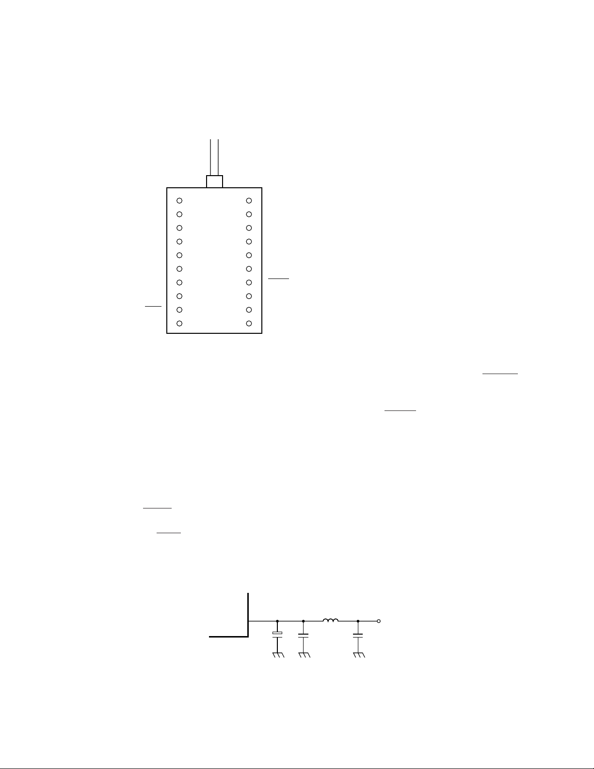
Connection Diagram
Top View
FIBER PIGTAIL
GND
GND
GND
GND
NC
GND
DATA
GND
DATA
PD BIAS
1
2
3
4
5
6
7
8
9
10
Pin Descriptions
Pins 5, 17, 18, 19, 20 NC:
These pins are not connected and
should be left open circuit on the
application PCB.
Pins 1, 2, 3, 4, 6, 8, 13, 15, 16
GND:
These pins should be connected
to the circuit ground.
Pins 7, 9, DATA, DATA:
These pins provide complementary PECL DATA and DATA
outputs. The DATA output is
noninverting, an optical pulse
causes the DATA output to go to
the PECL logic high state (+4 V
nominal).
20
19
18
17
16
15
14
13
12
11
NC
NC
NC
NC
GND
GND
ALARM
GND
ALARM
+5 V
Pin 10, PD Bias:
This pin must be connected to
any voltage from 0 V (GND) to
-5 V. This provides the
photodiode bias. The current
drawn is directly proportional
to the average received
photocurrent.
I = Responsitivity x Mean Power.
The responsivity will be between
0.7 A/W and 1.0 A/W.
Pin 11, +5 V:
This pin should be connected to
+5 V supply. The network shown
below should be placed as close
as possible to pin 11.
Pins 12, 14 ALARM, ALARM:
These pins provide complementary differential ALARM and
ALARM outputs. This is the low
light alarm. ALARM goes to a
logic low (3.3 V nominal) state
when the optical power drops
below the threshold level
(insufficient optical power).
The optical power must increase
to a higher level than the level
where the alarm went low before
ALARM will return to a logic
high. This difference is the alarm
hysteresis.
PIN 11
1 µH
100 nF 100 nF10 µF
+5 V
419
Page 3

Functional Description
Design
The receiver contains an InGaAsP
photodetector, transimpedance
amplifier and interface amplifier
circuit. It is designed with a
multimode fiber pigtail to allow
maximum flexibility in connector
options.
The interface amplifier is
capacitively coupled to the
preamplifier circuit.
Terminating the Outputs
The data outputs of the RCV1551
are PECL compatible. Care
should be taken to match
termination impedances to the
interconnect to minimize
reflection effects. Both serial data
outputs (DATA and DATA) should
be terminated identically, even if
only one output is used, in order
to balance the drive currents
drawn from the module. This will
lower the power supply noise
generated by the receiver and
improve performance at low
optical input power levels.
Power Supplies
The RCV1551 will operate to
specifications with a single +5 V
power supply (Pin 10 Grounded).
The -5 V PIN bias is provided to
maintain functional compatibility
with second sources.
Circuit Layout
The RCV1551 uses very high
bandwidth circuitry to achieve its
high level of performance. Care
must be taken to ensure stable
operation. The use of ground
planes and transmission line
interconnects is required. The use
of a standard evaluation board is
highly recommended for those
users who are not familiar with
these techniques.
Signal traces should conform to
ECL design rules to prevent
reflections and ringing from
degrading performance. Useful
guidelines are contained in ECL
manufacturer design manuals.
Manufacturing
The fiber pigtail on the device
requires normal fiber handling
considerations. Care should be
taken to avoid tight bends as well
as excessive tension on the fiber
pigtail.
The allowable temperature range
for the RCV1551 is limited by the
material used in the pigtail.
Exposure to temperatures over
+85°C is not recommended. Low
profile sockets and hand
soldering are recommended for
this part.
TRANSIMPEDANCE
AMPLIFIER
V NEG
(-5 V OR GROUND)
Figure 1. Block Diagram.
VCC (+5 V)
LOW PASS FILTER
GND (0 V)
INTERFACE
AMPLIFIER
ALARM
ALARM
DATA
DATA
420
Page 4

Performance Specifications Absolute Limiting Ratings
Absolute maximum limits mean that no catastrophic damage will occur if the product is subjected to these ratings for short periods, provided that each limiting
parameter is in isolation and all other parameters have values within the performance specification. It should not be assumed that limiting values of more than
one parameter can be applied to the product at the same time.
Parameter Symbol Minimum Maximum Units Note
Supply Voltage V
Supply Voltage V
CC
NEG
-0.5 +5.5 V 1
-10 +0.5 V -
Environmental Parameters
Parameter Symbol Minimum Maximum Units Note
Operating Temperature - -40 +85 °C-
Storage Temperature - -40 +85 °C-
Humidity - - 85 %RH -
Electrical Parameters (-40°C to +85°C)
Parameter Symbol Minimum Maximum Units Note
Supply Voltage V
Supply Voltage V
CC
NEG
VCC Supply Current - - 130 mA 4
V
Supply Current - - 1.0 mA -
NEG
DATA Output Level (high) - 3.8 4.15 V 2, 3
DATA Output Level (low) - 3.1 3.5 V 2, 3
ALARM Output Level (high) V off 3.8 4.15 V 2, 3
ALARM Output Level (low) V on 3.1 3.5 V 2, 3
Notes:
1. VCC of -0.5 V and V
2. Output terminated to (VCC -2) with 50 Ω load or equivalent.
3. Output voltages are for VCC = 5.0 V.
4. Outputs not loaded.
of +0.5 V may not be applied simultaneously.
NEG
4.75 5.25 V 0 -6.0 V -
421
Page 5

Optical Parameters (-40°C to +85°C)
Parameter Minimum Maximum Units Note
Wavelength 1200 1600 nm Receiver Sensitivity - -35 dBm 1
Maximum Input Power 0 - dBm Alarm ON -45 -36 dBm Hysteresis 0.5 7.0 dB Alarm Response Time - 600 µSReliability Target - 1000 FIT -
Note:
1. At a BER of 1 x 10
-10
23-1
, 2
PRBS pattern NRZ data at the line rate with 10:1 extinction ratio. EOL.
Fiber Pigtail Typical Units
Core Diameter 50 microns
Cladding Diameter 125 microns
Secondary Coating Diameter 900 microns
Drawing Dimensions
L
B A
J
H
K
DIM. MAX.
A
B
C
D
E
F
∅G
H
J
K
L
ALL DIMENSIONS IN MILLIMETERS
MIN. NOM.
32.9
9.9
16.0
–
2.26
–
–
2.7
5.2
–
400
–
–
–
–
–
2.54
0.46
–
–
10.16
–
33.1
10.1
16.3
9.27
2.62
–
–
3.2
5.6
–
1220
20 11
C
110
D
F∅G
E
422
Page 6

Ordering Information
RCV1551 - XX
Handling Precautions
1. The RCV1551 can be damaged
by current surges or
overvoltage. Power supply
transient precautions should
be taken.
2. Normal handling precautions
for electrostatic sensitive
devices should be taken.
Connector:
FP = FC/PC Polish
ST = ST®*
SC = SC
DN = DN
Model Name:
RCV1551
*ST® is a registered trademark of AT&T.
423
 Loading...